CYStech Electronics Corp.
Spec. No. : C154S6R
Issued Date : 2005.01.13
Revised Date :
Page No. : 1/6
HBCA143TS6R
CYStek Product Specification
PNP and NPN Dual Digital Transistors
HBCA143TS6R
Features
∑
Built-in bias resistors enable the configuration of an inverter circuit without connecting external input
resistors (see equivalent circuit).
∑
The bias resistors consist of thin-film resistors with complete isolation to allow positive biasing of the
input for PNP transistor, and negative biasing of the input for NPN transistor. They also have the
advantage of almost completely eliminating parasitic effects.
∑
Only the on/off conditions need to be set for operation, making device design easy.
∑
One DTA143T chip and one DTC143T chip in a SOT-363 package.
∑
Mounting by SOT-323 automatic mounting machines is possible.
∑
Mounting cost and area can be cut in half.
∑
Transistor elements are independent, eliminating interference
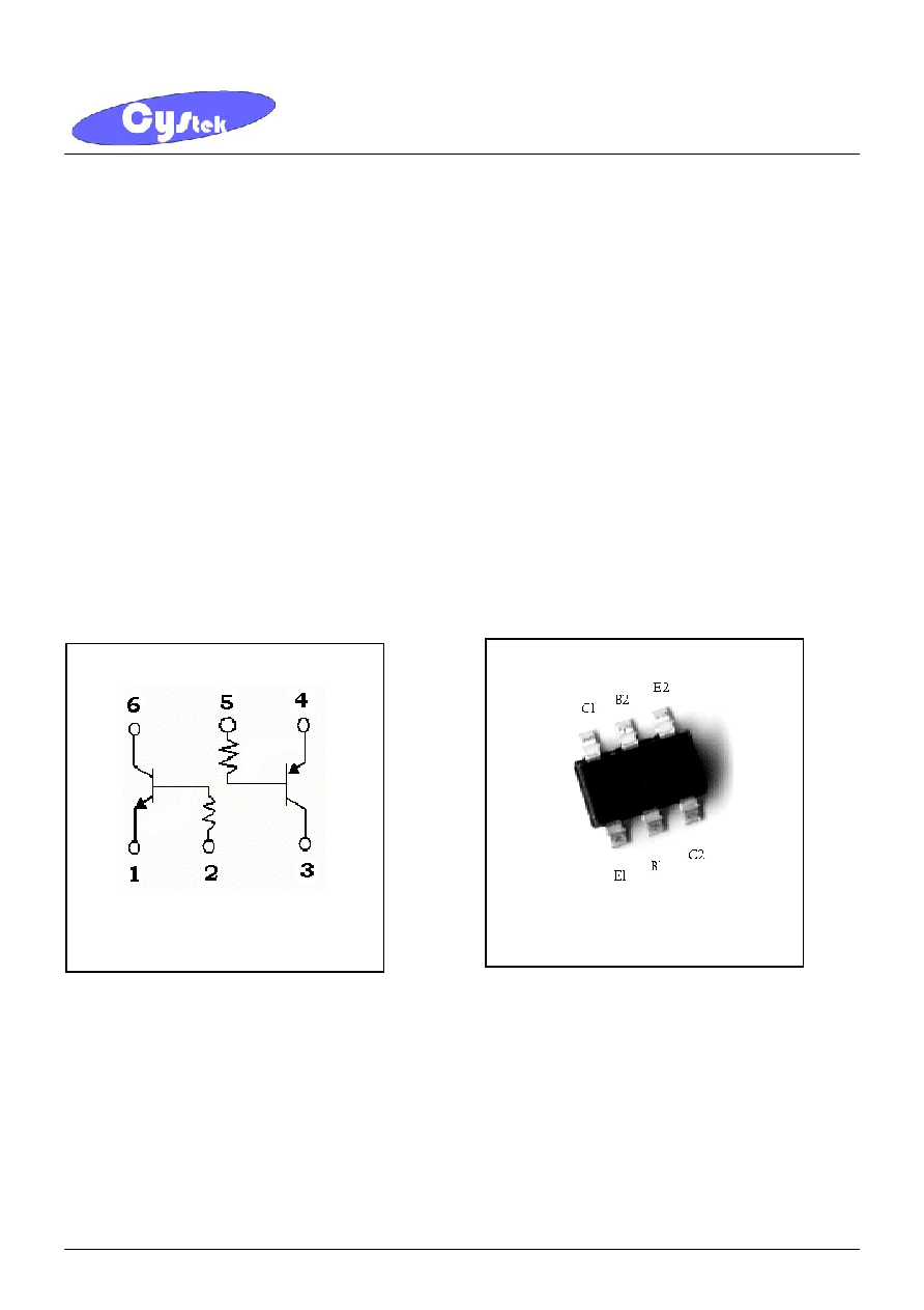
Equivalent Circuit Outline
SOT-363R
HBCA143TS6R
R
B
1=4.7k
, R
B
2=4.7 k
TR1 TR2
R
B
1
R
B
2

CYStech Electronics Corp.
Spec. No. : C154S6R
Issued Date : 2005.01.13
Revised Date :
Page No. : 2/6
HBCA143TS6R
CYStek Product Specification
Absolute Maximum Ratings
(Ta=25)
Limits
Parameter Symbol
Tr1(NPN) Tr2(PNP)
Unit
Collector-Base Voltage
V
CBO
50
-50
V
Collector-Emitter Voltage
V
CEO
50
-50
V
Emitter-Base Voltage
V
EBO
5
-5
V
Collector Current
I
C
100
-100
mA
Total Power Dissipation
Pd
200 (Note)
mW
Junction Temperature
Tj
150
∞
C
Storage Temperature
Tstg
-55~+150
∞
C
Note : 150mW per element must not be exceeded.
Characteristics
(Ta=25)
∑Tr1(NPN)
Parameter Symbol
Min
Typ Max Unit
Test
Conditions
Collector-Base Breakdown Voltage
V
CBO
50 -
- V I
C
=50µA
Collector-Emitter Breakdown Voltage
V
CEO
50 -
- V
I
C
=1mA
Emitter-Base Breakdown Voltage
V
EBO
5 -
- V
I
E
=50µA
Collector-Base Cutoff Current
I
CBO
- -
0.5
µA
V
CB
=50V
Emitter-Base Cutoff Current
I
EBO
- -
0.5
µA
V
EB
=4V
Collector-Emitter Saturation Voltage
V
CE(sat)
- -
0.3
V
I
C
=5mA, I
B
=0.25mA
DC Current Gain
h
FE
100 -
600
- V
CE
=5V, I
C
=1mA
Input Resistance
R
3.29
4.7
6.11
k
-
Transition Frequency
fT
-
250
-
MHz V
CE
=10V, I
E
=5mA, f=100MHz*
* Transition frequency of the device
∑Tr2(PNP)
Parameter Symbol Min. Typ. Max. Unit
Test
Conditions
Collector-Base Breakdown Voltage
BV
CBO
-50
-
- V
I
C
=-50µA
Collector-Emitter Breakdown Voltage
BV
CEO
-50
-
- V
I
C
=-1mA
Emitter-Base Breakdown Voltage
BV
EBO
-5 -
- V
I
E
=-50µA
Collector-Base Cutoff Current
I
CBO
- -
-0.5
µA
V
CB
=-50V
Emitter-Base Cutoff Current
I
EBO
- -
-0.5
µA
V
EB
=-4V
Collector-Emitter Saturation Voltage
V
CE(sat)
- 0.1
-0.3
V I
C
=-5mA, I
B
=-0.25mA
DC Current Gain
h
FE
100
- 600
- V
CE
=-5V, I
C
=-1mA
Input Resistance
R
3.29
4.7
6.11
k
-
Transition Frequency
f
T
-
250
-
MHz V
CE
=-10V, I
C
=-5mA,f=100MHz *
* Transition frequency of the device
CYStech Electronics Corp.
Spec. No. : C154S6R
Issued Date : 2005.01.13
Revised Date :
Page No. : 3/6
HBCA143TS6R
CYStek Product Specification
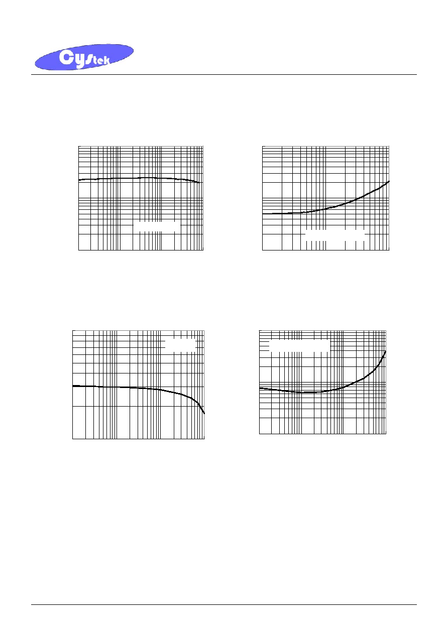
Characteristic Curves
∑Tr1(
NPN)
Current Gain vs Collector Current
10
100
1000
0.1
1
10
100
Collector Current --IC(mA)
Current Gain---
HFE
HFE@VCE=5V
Saturation Voltage vs Collector Current
10
100
1000
1
10
100
Collector Current --- IC(mA)
Saturation Voltage---(mV)
VCESAT@IC=20IB
∑Tr2(
PNP)
Current Gain vs Collector Current
100
1000
0.1
1
10
100
Collector Current---IC(mA)
Current Gain---HFE
VCE=5V
Saturation Voltage vs Collector Current
10
100
1000
0.1
1
10
100
Collector Current---IC(mA)
Saturation Voltage---(mV)
VCE(SAT)@IC=20IB
CYStech Electronics Corp.
Spec. No. : C154S6R
Issued Date : 2005.01.13
Revised Date :
Page No. : 4/6
HBCA143TS6R
CYStek Product Specification
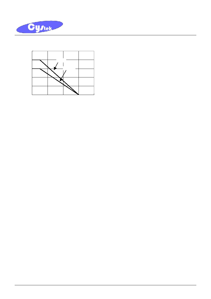
Power Derating Curves
0
50
100
150
200
250
0
50
100
150
200
Ambient Temperature
---
T
A
()
Power Dissipation---P
D
(mW)
Dual
Single

CYStech Electronics Corp.
Spec. No. : C154S6R
Issued Date : 2005.01.13
Revised Date :
Page No. : 5/6
HBCA143TS6R
CYStek Product Specification
Reel Dimension
Carrier Tape Dimension
CYStech Electronics Corp.
Spec. No. : C154S6R
Issued Date : 2005.01.13
Revised Date :
Page No. : 6/6
HBCA143TS6R
CYStek Product Specification
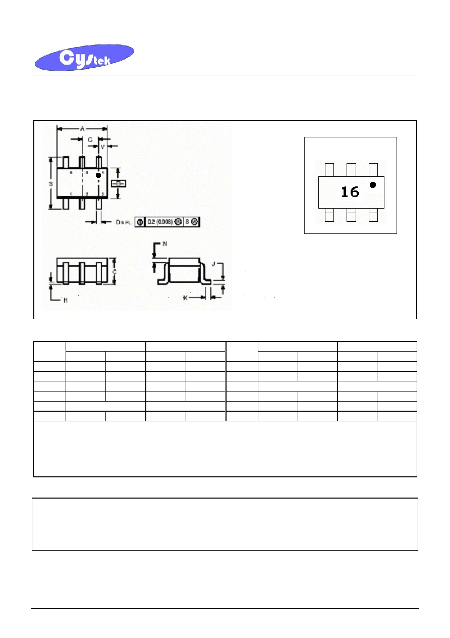
SOT-363 Dimension
*:Typical
Inches Millimeters
Inches Millimeters
DIM
Min. Max. Min. Max.
DIM
Min. Max. Min. Max.
A 0.071 0.087 1.8 2.2 J 0.004 0.010 0.1 0.25
B 0.045 0.053 1.15 1.35 K 0.004 0.012 0.1 0.30
C
0.031
0.043
0.8
1.1
N
0.008 REF
0.20 REF
D 0.004 0.012 0.1 0.3 S 0.079 0.087 2.00 2.20
G 0.026BSC
0.65BSC Y
0.012
0.016
0.30
0.40
H
-
0.004
-
0.1
Notes : 1
.Controlling dimension : millimeters.
2.Maximum lead thickness includes lead finish thickness, and minimum lead thickness is the minimum thickness of base material.
3.If there is any question with packing specification or packing method, please contact your local CYStek sales office.
Material :
∑
Lead : 42 Alloy ; solder plating
∑
Mold Compound : Epoxy resin family, flammability solid burning class:UL94V-0
Important Notice:
∑
All rights are reserved. Reproduction in whole or in part is prohibited without the prior written approval of CYStek.
∑
CYStek reserves the right to make changes to its products without notice.
∑
CYStek semiconductor products are not warranted to be suitable for use in Life-Support Applications, or systems.
∑
CYStek assumes no liability for any consequence of customer product design, infringement of patents, or application assistance.
6-Lead SOT-363R Plastic
Surface Mounted Package
CYStek Package Code: S6R
Style:
Pin 1. Emitter1 (E1)
Pin 2. Base1 (B1)
Pin 3. Collector2 (C2)
Pin 4. Emitter2 (E2)
Pin 5. Base2 (B2)
Pin 6. Collector1 (C1)
Marking: