CYStech Electronics Corp.
Spec. No. : C515M3
Issued Date : 2003.04.02
Revised Date : 2005.01.11 .
Page No. : 1/4
LM78L05XM3
CYStek Product Specification
Low Current Positive Voltage Regulator
LM78L05XM3
Description
The LM78L05XM3 series of surface mount regulators are easy-to-
use devices suitable for multitude of applications that require a regulated supply of up to 100mA. These regulators
feature internal current limiting and thermal shutdown, making them remarkably rugged. No external components are
required with the LM78L05XM3 devices in many applications.
These devices offer a substantial performance advantage over the traditional zener diode resistor combination, as
output impedance and quiescent current are substantially reduced.
Features:
∑
Wide Range Of Available, Fixed Output Voltages
∑
Internal Short-Circuit Current Limiting
∑
Internal Thermal Overload Protection
∑
No External Components Required
∑
Pb-free package
Absolute Maximum Ratings
(Ta=25
∞
C)
∑
Input Voltage....................................................................................................................................................... 30 V
∑
Total Power Dissipation.................................................................................................................. Internally limited
∑
Operating Temperature Range .......................................................................................................... 0
∞
C to +125
∞
C
∑
Maximum Junction Temperature ..................................................................................................................... 125
∞
C
∑
Storage Temperature Range ........................................................................................................... -55
∞
C to +150
∞
C
∑
Lead Temperature (Soldering 10S).................................................................................................................. 260
∞
C
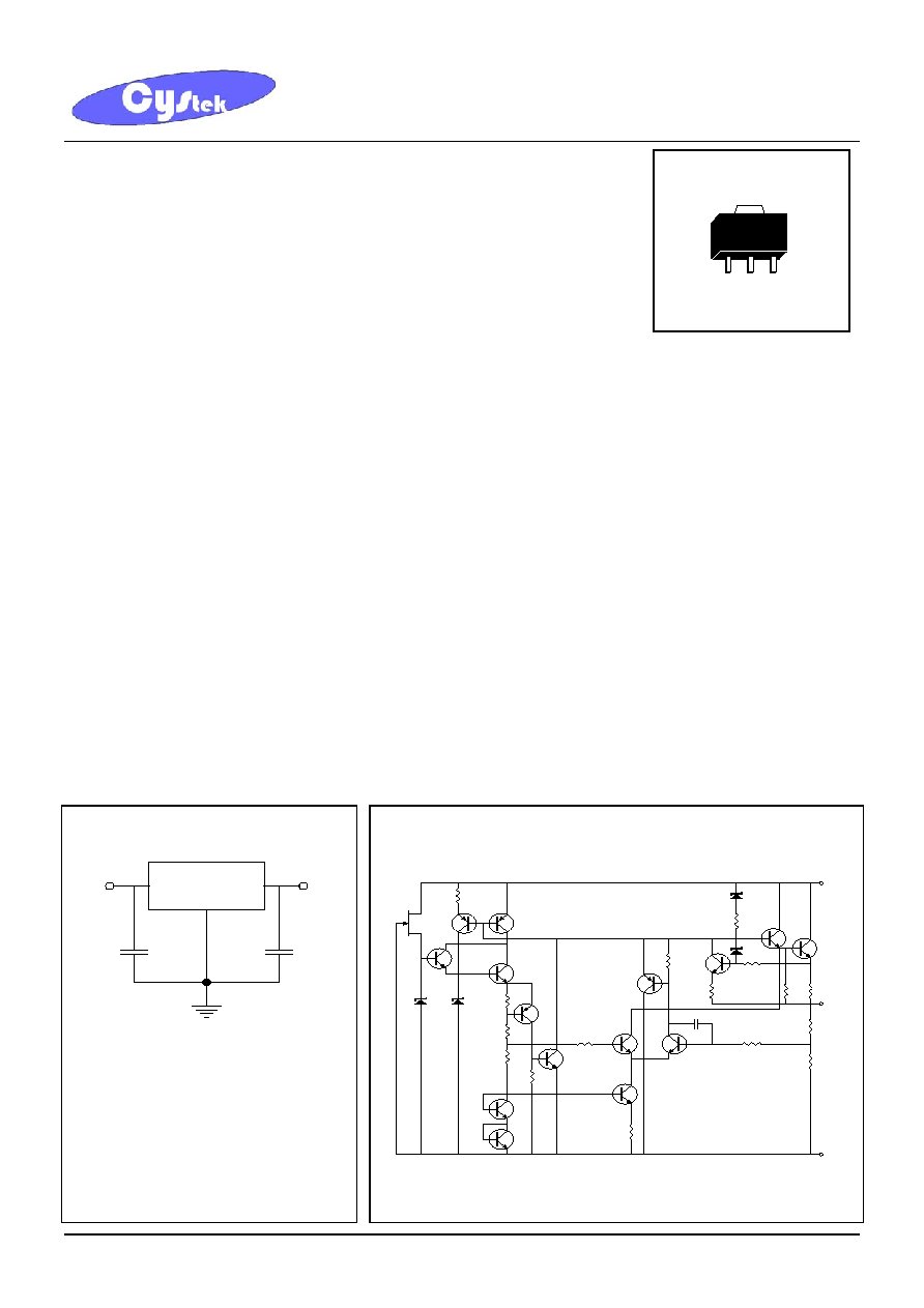
Typical Application
Schematic Diagram
LM78L05
Vout
Vin
1
3
2
C1 C2
A common ground is required between the
input and the output
voltages. The
input
voltage must remain typically
2.0V
above
the output voltage even during the low point
on the input ripple
voltage.
Note : C1 and C2 are required if regulator is located
far from power supply filter and load, or oscillation
may induced on the loop.
576
3.41K
3.89K
7.8K
2.84K
13K
5pF
2.23K
GND
1.5K
1.9K
100
100
5K
5.7K
Vout
Vin
SOT-89
O G I
CYStech Electronics Corp.
Spec. No. : C515M3
Issued Date : 2003.04.02
Revised Date : 2005.01.11 .
Page No. : 2/4
LM78L05XM3
CYStek Product Specification
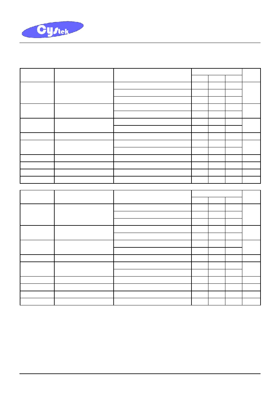
Electrical Characteristics
Vin=10V, Io=40mA, Tj=25
∞
C Cin=0.33uF, Cout=0.1uF (unless otherwise noted)
LM78L05A
Symbol Parameter
Conditions
Min Typ Max
Units
Tj=25
∞
C
4.85 5 5.15
7V
Vin
25V, 1mA
Io
40mA
4.75 5 5.25
Vo Output
Voltage
1mA
Io
70mA
4.75 5 5.25
V
7V
Vin
20V
- -
150
Vo
Line Regulation
8V
Vin
20V
- -
100
mV
1mA
Io
100mA
- - 60
Vo
Load Regulation
1mA
Io
40mA
- - 30
mV
IQ Quiescent
Current Ta=25
∞
C
- - 5 mA
8V
Vin
20V
- - 1
IQ
Quiescent Current
Change
1mA
Io
40mA
- - 0.1
mA
Vn Output
Noise
Voltage
10Hz
f
100KHz
- 40 - uV
Vin /
Vout Ripple Rejection
8V
Vin
16V, f=120Hz
47 62 - dB
Ipk
Peak Output Current
Ta=25
∞
C
- 140 - mA
VD Dropout
Voltage
Ta=25
∞
C
- 1.7 - V
LM78L05B
Symbol Parameter
Conditions
Min Typ Max
Units
Tj=25
∞
C
4.75 5 5.25
7V
Vin
25V, 1mA
Io
40mA
4.75 5 5.25
Vo Output
Voltage
1mA
Io
70mA
4.75 5 5.25
V
7V
Vin
20V
- -
150
Vo
Line Regulation
8V
Vin
20V
- -
100
mV
1mA
Io
100mA
- - 60
Vo
Load Regulation
1mA
Io
40mA
- - 30
mV
IQ Quiescent
Current Ta=25
∞
C
- - 5 mA
8V
Vin
20V
- - 1
IQ
Quiescent Current
Change
1mA
Io
40mA
- - 0.1
mA
Vn Output
Noise
Voltage
10Hz
f
100KHz
- 40 - uV
Vin /
Vout Ripple Rejection
8V
Vin
16V, f=120Hz
47 62 - dB
Ipk
Peak Output Current
Ta=25
∞
C
- 140 - mA
VD Dropout
Voltage
Ta=25
∞
C
- 1.7 - V
CYStech Electronics Corp.
Spec. No. : C515M3
Issued Date : 2003.04.02
Revised Date : 2005.01.11 .
Page No. : 3/4
LM78L05XM3
CYStek Product Specification
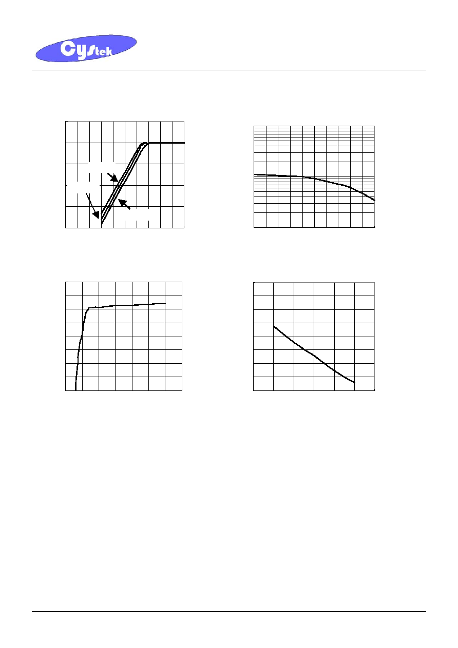
Characteristic Curves
Dropout Characteristics
1
2
3
4
5
6
0
1
2
3
4
5
6
7
8
9 10
Input Voltage(V)
Output
Voltage(V)
Io=100mA
Io=1mA
Io=40mA
Maximum Average Power Dissipation
100
1000
10000
25
50
75
100
125
150
Ambient Temperature (∞C)
Power Dissipation (mW)
Quiescent Current
0
0.5
1
1.5
2
2.5
3
3.5
4
0
5
10
15
20
25
30
35
Input Voltage(V)
Quiescent Current(mA)
Quiescent Current
2.6
2.8
3
3.2
3.4
0
50
100
150
Ambient Temperature(∞C)
Quiescent Current(mA)
CYStech Electronics Corp.
Spec. No. : C515M3
Issued Date : 2003.04.02
Revised Date : 2005.01.11 .
Page No. : 4/4
LM78L05XM3
CYStek Product Specification
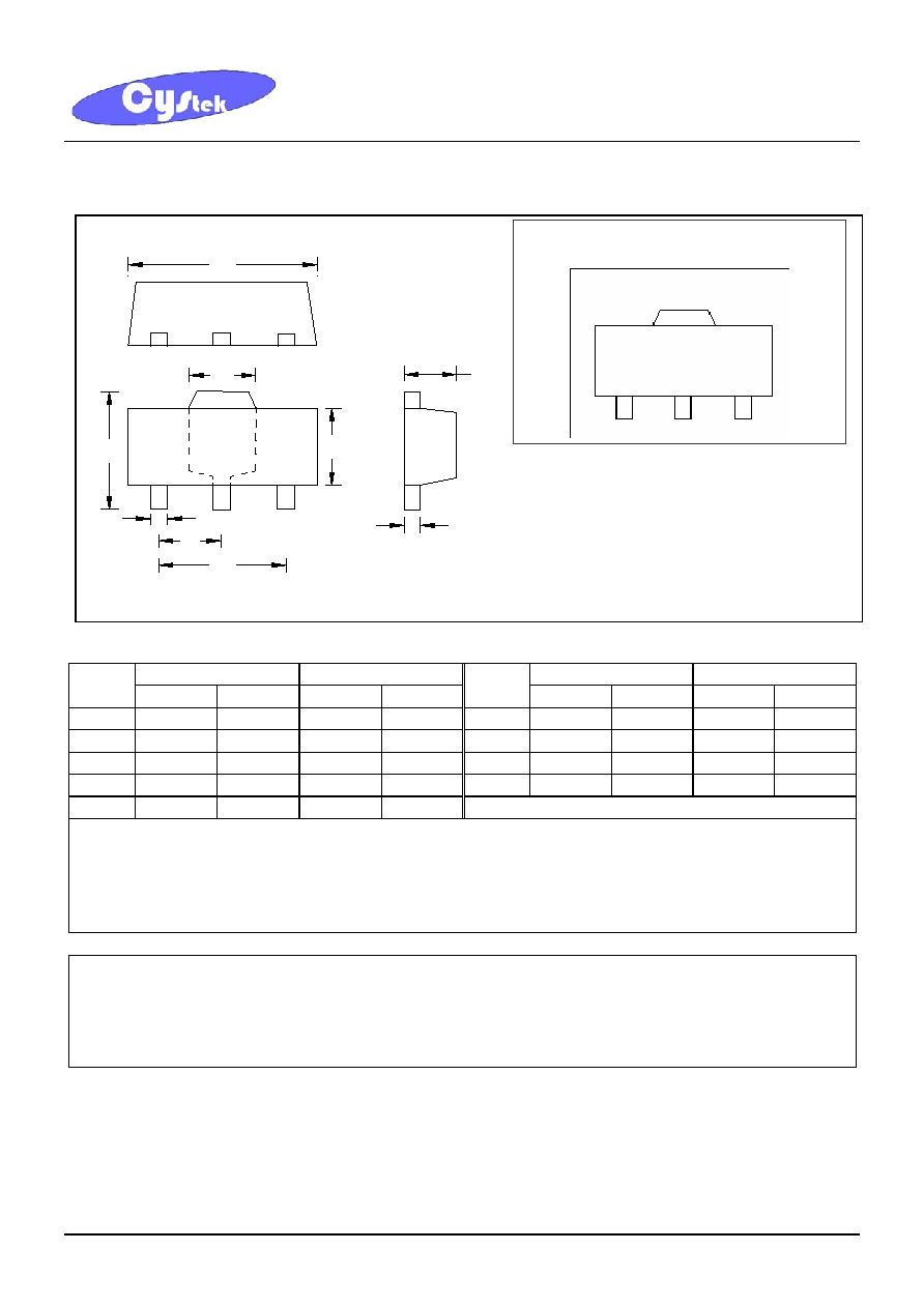
SOT-89 Dimension
*: Typical
Inches Millimeters
Inches Millimeters
DIM
Min. Max. Min. Max.
DIM
Min. Max. Min. Max.
A 0.1732
0.1811
4.40 4.60 F 0.0583
0.0598 1.48 1.527
B 0.1594
0.1673 4.05 4.25 G 0.1165
0.1197 2.96 3.04
C 0.0591
0.0663 1.50 1.70 H 0.0551
0.0630 1.40 1.60
D 0.0945
0.1024 2.40 2.60 I 0.0138
0.0161 0.35 0.41
E 0.01417
0.0201 0.36 0.51
Notes:
1.Controlling dimension: millimeters.
2.Maximum lead thickness includes lead finish thickness, and minimum lead thickness is the minimum thickness of base material.
3.If there is any question with packing specification or packing method, please contact your local CYStek sales office.
Material:
∑
Lead: 42 Alloy ; solder plating
∑
Mold Compound: Epoxy resin family, flammability solid burning class: UL94V-0
Important Notice:
∑
All rights are reserved. Reproduction in whole or in part is prohibited without the prior written approval of CYStek.
∑
CYStek reserves the right to make changes to its products without notice.
∑
CYStek semiconductor products are not warranted to be suitable for use in Life-Support Applications, or systems.
∑
CYStek assumes no liability for any consequence of customer product design, infringement of patents, or application assistance.
78L05
3-Lead SOT-89 Plastic
Surface Mounted Package
CYStek Package Code: M3
E
F
G
C
B
A
I
D
H
3
2
1
Marking:
Style: Pin 1. Vout 2. GND 3. Vin
78L05