CYStech Electronics Corp.
Spec. No. : C540J3
Issued Date : 2003.06.25
Revised Date :
Page No. : 1/4
PL1085J3
CYStek Product Specification
3A Low Dropout Positive Voltage Regulator
PL1085-XXXJ3
Features
Dropout Voltage 1.3V at 3A Output Current.
Fast Transient Response.
Extremely Tight Line and Load Regulation.
Current Limiting and Thermal Protection.
Adjustable Output Voltage or Fixed 1.5V, 1.8V, 2.5V, 2.85, 3.0V, 3.3V, 3.5V, 5.0V.
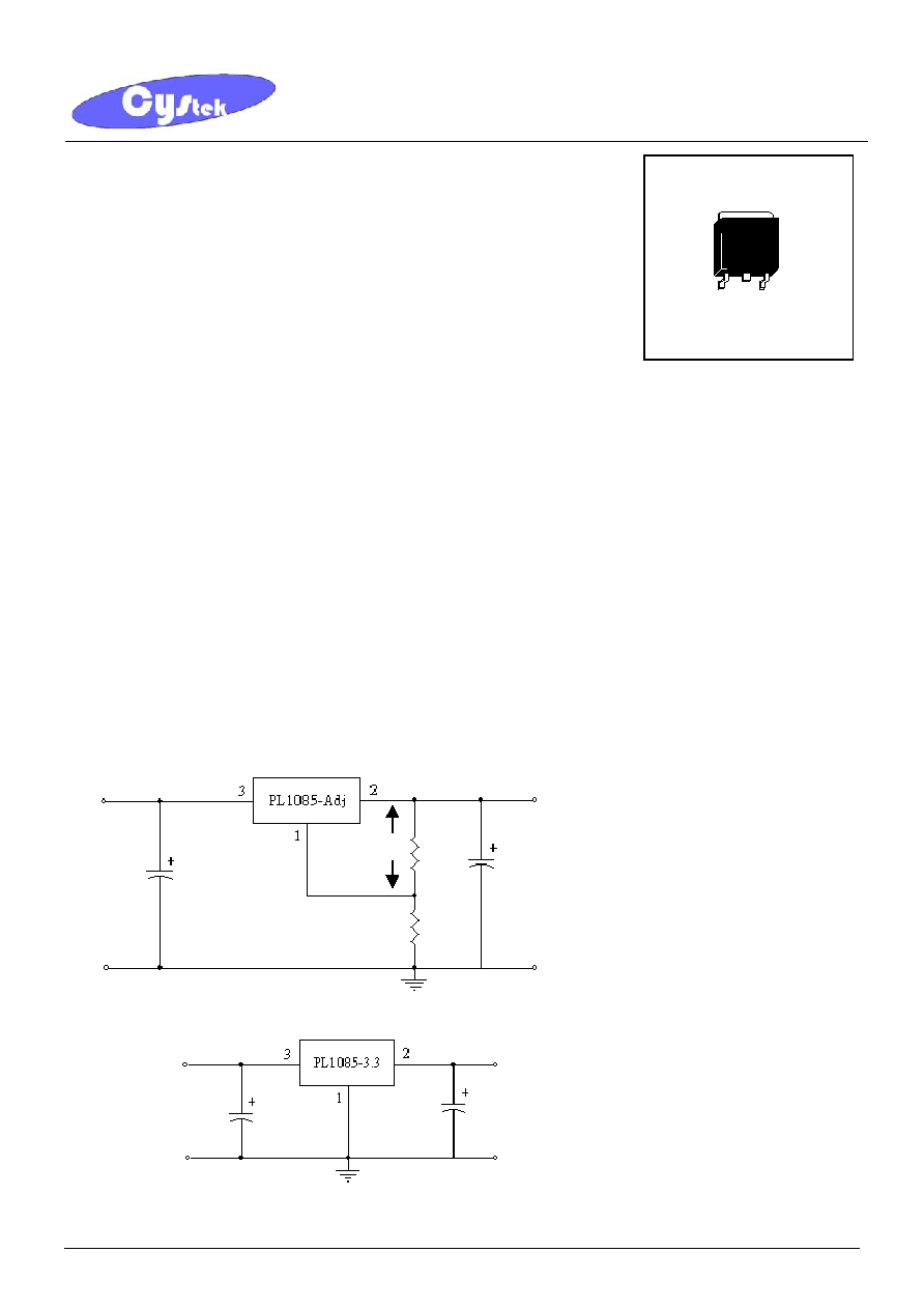
Standard 3-Pin Power Packa
ges.
Description
The PL1085-XXXJ3 is a low dropout three terminal regulator with 3A output current capability. The output voltage is
adjustable with the use of a resistor divider or fixed 1.5V, 1.8V, 2.5V, 2.85V, 3.0V, 3.3V, 3.5V and 5.0V. Dropout voltage is
guaranteed to be at maximum of 1.3V with the maximum output current. Its low dropout voltage and fast transient response
make it ideal for low voltage microprocessor applications. Current limit and thermal protection provide protection against
any overload condition that would create excessive junction temperatures.
Applications
Mother Board I/O Power Supplies.
Microprocessor Power Supplies.
High Current Regulator.
Post Regulator for Switching Supply.
Typical Application Circuit
TO-252
VREF
Vin=5V
Vout=3.3V
C2
10F
R1
125
1%
R2
205
1%
C1
10F
ADJ
Adjustable Voltage Regulator
GND
V
REF
=V
OUT
-V
ADJ
=1.25V(typ)
V
OUT
=V
REF
(1+R
1
/R
2
)+I
ADJ
◊R
2
I
ADJ
=55µA(typ.)
(1) C1 needed if device is far
away from filter capacitors.
(2)C2 required for stability.
C2
10F
C1
10F
Fixed Voltage Regulator
Vout=3.3V
Vin=5V
CYStech Electronics Corp.
Spec. No. : C540J3
Issued Date : 2003.06.25
Revised Date :
Page No. : 2/4
PL1085J3
CYStek Product Specification
Ordering Information
Device
Output Voltage
Device
Output Voltage
PL1085-AdjJ3 Adjustable
PL1085-3.0J3 3.0V
PL1085-1.5J3 1.5V
PL1085-3.3J3
3.3V
PL1085-1.8J3 1.8V
PL1085-3.5J3
3.5V
PL1085-2.5J3 2.5V
PL1085-5.0J3
5.0V
PL1085-2.85J3 2.85V
Absolute Maximum Ratings
VIN pin to ADJ/GND pin .............................................................................................................7V
Operating Junction Temperature Range .................................................................................0∞C~ 125∞C
Storage Temperature Range............................................................................................- 65∞C ~ 150∞C
Thermal Resistance Junction to Case ........................................................................................12.5∞C /W
Thermal Resistance Junction to Ambient (Assume no ambient airflow, no heatsink) ................................ 100∞C /W
Lead Temperature (Soldering) 10 sec. ...........................................................................................260∞C
Electrical Characteristics
(Vin=5V, Io=10mA,Tj=25,unless otherwise noted)
Symbol Parameter
Conditions Min
Typ
Max
Units
V
REF
Reference
Voltage
Tj=25
∞
C
1.238 1.250 1.262
V
Vo Output
Voltage
PL1085-1.5
PL1085-1.8
PL1085-2.5
PL1085-2.85
PL1085-3.0
PL1085-3.3
PL1085-3.5
PL1085-5.0
1.48
1.78
2.47
2.82
2.97
3.26
3.46
4.95
1.50
1.80
2.50
2.85
3.00
3.30
3.50
5.00
1.52
1.82
2.53
2.88
3.03
3.34
3.54
5.05
V
Adj : 2.65V
Vin
7V,Tj=25
Vo
Line Regulation
Fix : 1.4+Vout
Vin
7V
- 0.015 0.2 %
Vo
Load Regulation
10mA
Io
3A,Tj=25 -
-
0.6
%
Is Current
Limit
Vin-Vout=1.5V
3 - - A
I
Adj
Adjust Pin Current
2.65V
Vin
7V
- 55 90 A
I
Adj
Adjust Pin Current
Change
2.65V
Vin
7V, 0
∞
C
Tj
125
∞
C
- 0.2 5 A
Ts Temperature
Stability
Io=0.5A, 0
∞
C
Tj
125
∞
C
- 0.5 - %
I
L
Minimum Load Current
0
∞
C
Tj
125
∞
C
- 5 10 mA
V
N
RMS Output Noise(% of Vout) 10Hz
f
10KHz,Tj=25
- 0.003 -
%
RR
Ripple Rejection Ratio
Vin-Vout=3V, f=120Hz,
Cout=25F
60 72 - dB
V
D
Dropout
Voltage
Vout ,
V
REF
=1%,
10mA
Io
3A
0
∞
C
Tj
125
∞
C
- 1.2 1.3 V
CYStech Electronics Corp.
Spec. No. : C540J3
Issued Date : 2003.06.25
Revised Date :
Page No. : 3/4
PL1085J3
CYStek Product Specification
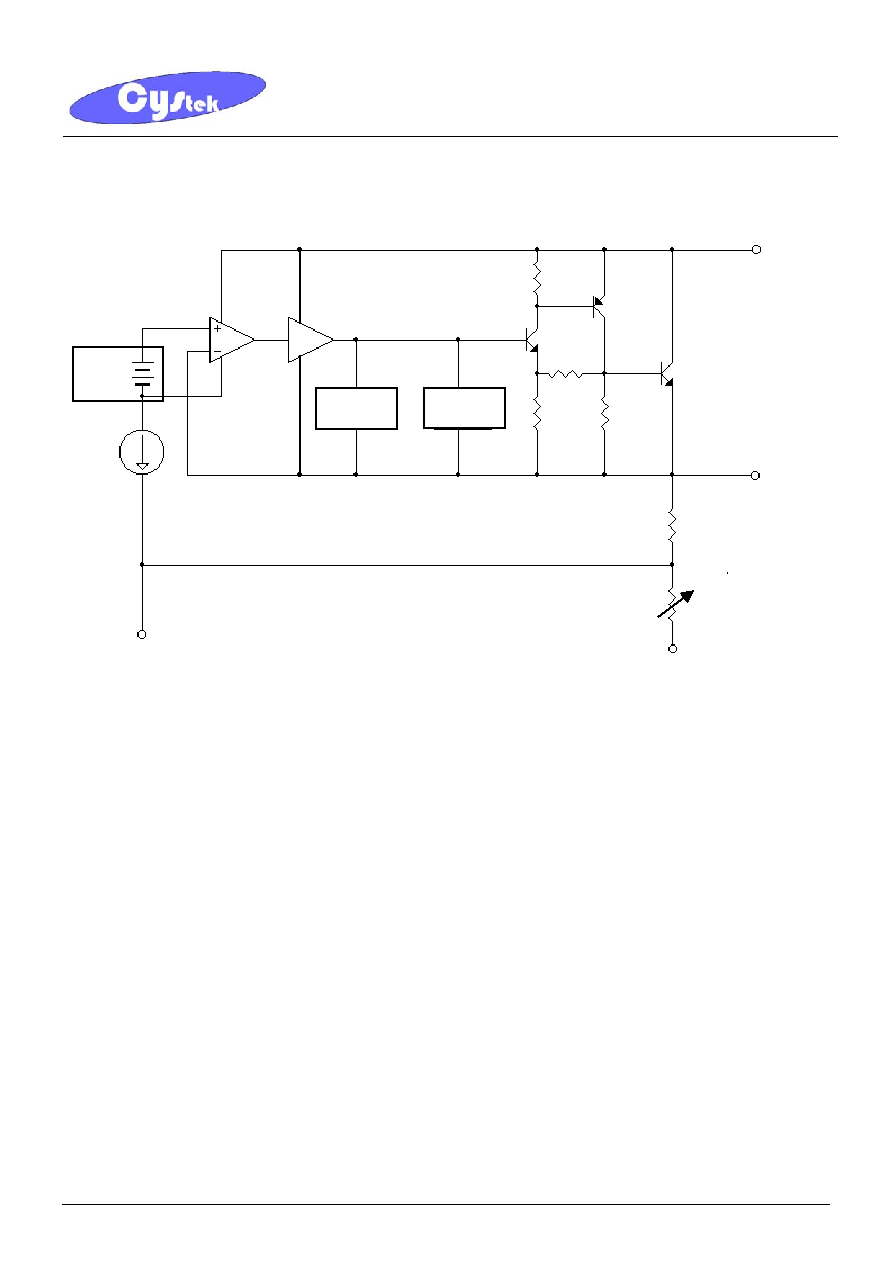
Block Diagram
ADJ
GND
VOUT
VIN
55A
V
REF
1.25V
Current Amp.
Thermal
Limit
Current
Limit
For fixed voltage
device
CYStech Electronics Corp.
Spec. No. : C540J3
Issued Date : 2003.06.25
Revised Date :
Page No. : 4/4
PL1085J3
CYStek Product Specification
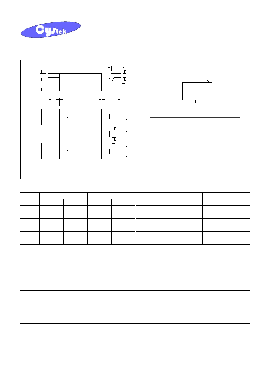
TO-252 Dimension
*: Typical
Inches Millimeters
Inches Millimeters
DIM
Min. Max. Min. Max.
DIM
Min. Max. Min. Max.
A 0.0177
0.0217 0.45 0.55 G 0.0866 0.1102 2.20 2.80
B 0.0650
0.0768
1.65 1.95 H - *0.0906 - *2.30
C
0.0354
0.0591
0.90 1.50 I - 0.0354 - 0.90
D
0.0177
0.0236
0.45 0.60 J - 0.0315 - 0.80
E 0.2520
0.2677 6.40 6.80 K 0.2047 0.2165 5.20 5.50
F 0.2125
0.2283 5.40 5.80 L 0.0551 0.0630 1.40 1.60
Notes:
1.Controlling dimension: millimeters.
2.Maximum lead thickness includes lead finish thickness, and minimum lead thickness is the minimum thickness of base material.
3.If there is any question with packing specification or packing method, please contact your local CYStek sales office.
Material:
∑
Lead: 42 Alloy; solder plating
∑
Mold Compound: Epoxy resin family, flammability solid burning class: UL94V-0
Important Notice:
∑
All rights are reserved. Reproduction in whole or in part is prohibited without the prior written approval of CYStek.
∑
CYStek reserves the right to make changes to its products without notice.
∑
CYStek semiconductor products are not warranted to be suitable for use in Life-Support Applications, or systems.
∑
CYStek assumes no liability for any consequence of customer product design, infringement of patents, or application assistance.
B
A
C
E
H
I
J
K
3
2
1
D
F
G
L
Style: Pin 1.Adj(GND) 2.Vout(TAB) 3.Vin
3-Lead TO-252 Plastic Surface Mount Package
CYStek Package Code: J3
Marking:
1085-XXX