
CYStech Electronics Corp.
Spec. No. : C503Q8
Issued Date : 2003.03.21
Revised Date :
Page No. : 1/5
PL2951Q8
CYStek Product Specification
100mA Low Dropout Voltage Regulators
PL2951-XXQ8
FEATURES APPLICATIONS
∑
Battery powered systems
∑
High accuracy output voltage
∑
Cordless telephones
∑
Guaranteed 100mA output
∑
Radio control systems
∑
Very low quiescent current
∑
Portable/Palm top/Notebook computers
∑
Low dropout voltage
∑
Portable consumer equipment
∑
Extremely tight load and line regulation
∑
Portable Instrumentation
∑
Very low temperature coefficient
∑
Avionics
∑
Needs only 1
µ
F for stability
∑
Automotive Electronics
∑
Error Flag warns of output dropout
∑
SMPS Post-Regulator
∑
Logic-Controlled electronic shutdown
∑
Voltage Reference
∑
Output programmable from 1.24 to 29V
PRODUCT DESCRIPTION
The PL2951-XX is a low power voltage regulator. This device excellent choice for use in battery powered
application such as cordless telephone, radio control systems, and portable computers.
The PL2951-XX features very low quiescent current (75
µ
A Typ.) and very low drop output voltage (Typ.
40mV at light load and 380mV at 100mA). This includes a tight initial tolerance of 0.5% typ., extremely
good load and line regulation of 0.05% typ., and very low output temperature coefficient, making the
PL2951-XX useful as a low-power voltage reference.
The error flag output feature is used as power-on reset for warn of a low output voltage, due to following
batteries on input. Other feature is the logic-compatible shutdown input which enable the regulator to be
switched on and off.
The PL2951-XX is available in 8-pin plastic packages. The regulator output voltage may be pin-strapped
for a -XX volt or programmed from 1.24 volt to 29 volts with external pair of resistors.
Absolute Maximum Ratings
Pin Connection
Power Dissipation
Internally Limited
Lead Temperature
(Soldering, 5 seconds)
260
Storage Temperature Range
-65
∞
C to+150
∞
C
Operating Junction Temperature
Range
-55
∞
C to +150
∞
C
Input Supply Voltage
-0.3 to +30V
Feedback Input Voltage
-1.5 to +30V
Shutdown Input Voltage
-0.3 to +30V
Error Comparator Output
-0.3 to +30V
error

CYStech Electronics Corp.
Spec. No. : C503Q8
Issued Date : 2003.03.21
Revised Date :
Page No. : 2/5
PL2951Q8
CYStek Product Specification
Device Selection Guide
* - other versions are also available
Vout = 2.0V to 5.0V. Please consult factory for
more information
ELECTRICALCHARACTERISTICS (at Ta =25, =15V;unless otherwise noted
)
Parameter
Conditions(Note 2)
Min Typ Max Units
Output Voltage
-25T
J
85
Full Operating Temperature
0.985Vo
0.98Vo
Vo
1.015Vo
1.02Vo
Output Voltage
100AI
L
100mA,T
J
T
JMAX
0.976Vo
Vo
1.024Vo
V
Output Voltage Temperature
Coefficient
(Note 1)
-
50
150
ppm/
Line Regulation(Note 3)
V
O
+1VVin30V(Note 4)
- 0.04 0.4 %
Load Regulation(Note 3)
100AI
L
100mA
- 0.1 0.3 %
Dropout Voltage(Note 5)
I
L
=100A
I
L
=100mA
- 50
380
80
450
mV
Ground Current
I
L
=100A
I
L
=100mA
- 75
8
120
12
A
mA
Dropout Ground Current
Vin=Vo-0.5V,I
L
=100A
- 110
170 A
Current Limit
Vout=0
-
160
200
mA
Thermal Regulation
-
0.05
0.2
%/W
Output Noise, 10Hz to 100KHz C
L
=1F
C
L
=200F
C
L
=3.3F
(Bypass=0.01F, pins 7 to 1)
- 430
160
100
-
Vrms
Reference
Voltage
1.21 1.235 1.26
Reference Voltage
Over Temperature(Note 6)
1.185
-
1.285
V
Feedback Pin Bias Current
-
20
40
nA
Reference Voltage Temperature
Coefficient
(Note
7)
- 50 - ppm/
Feedback Pin Bias Current
Temperature Coefficient
- 0.1 - nA/
Error Comparator
Output Leakage Current
Voh=30V
-
0.01
1.0
A
Output Low Voltage
Vin=4.5V,I
OL
=400A
- 150
250
Upper Threshold Voltage
(Note 8)
40
60
-
Lower Threshold Voltage
(Note 8)
-
75
95
Hysteresis
(Note
8)
- 15 -
mV
Shutdown Input
Input Logic Voltage
Low(Regulator ON)
High(Regulator OFF)
-
2
1.3
-
0.7
-
V
Shutdown Pin Input Current
Vs=2.4V
Vs=30V
-
-
30
450
50
600
- - -
- 3 10
-
-
20
Regulator Output Current in
Shutdown
(Note 9)
V
OUT
=5V
3.3VV
OUT
5.0V
2.0VV
OUT
3.3V
-
-
30
A
Vout
, Volts
Device
2.85*
PL2951-2.85
3.0
PL2951-3.0
3.3
PL2951-3.3
5.0
PL2951-5.0

CYStech Electronics Corp.
Spec. No. : C503Q8
Issued Date : 2003.03.21
Revised Date :
Page No. : 3/5
PL2951Q8
CYStek Product Specification
Note 1:Output or reference voltage temperature coefficients defined as the worse case voltage change divided by the
total temperature range.
Note 2:Unless otherwise specified all limits guaranteed for T
J
=25,Vin=Vo+1V,I
L
=100A and C
L
=1F.
Feedback pin tied to
≠XX V tap pin and output tied to output sense (Vout=XX V) and V
shutdown
0.8V.
Note 3.Regulations is measured at constant junction temperature, using pulse testing with a low duty cycle.
Changes in output voltage due to heating effects are covered under the specification for thermal regulation.
Note 4:Line regulation is tested at 150 for I
L
=1mA. For I
L
=100A and T
J
=125 , line regulation is guaranteed
by design to 0.2%.
Note 5:Dropout voltage is defined as the input to output differential at which the output voltage drops 100mV below
its nominal value measured at 1V differential. At very low values of programmed output voltage, the mini-
mum input supply voltage of 2V(2.3V over temperature) must be taken into account.
Note 6:VrefVout(Vin-1V),2.3VVin30V,100AI
L
100mA,T
J
T
JMAX
.
Note 7:Output or reference voltage temperature coefficient is defined as the worst case voltage change divided by
the total temperature range.
Note 8:Comparator thresholds are expressed in terms of a voltage differential at the feedback terminal below the
nominal reference voltage measured at Vo+1V input. To express these thresholds in terms of output voltage
change, multiply by the error amplifier gain = Vout/Vin=(R1+R2)/R2. For example, at a programmed output
voltage of 5V, the error output is guaranteed to go low when the output drops by 95mV◊5V/1.235=384mV.
Thresholds remain constant as a percent of Vout as Vout is varied, with the dropout warning occurring at
typically 5% below nominal, 7.5% guaranteed.
Note 9:Vshutdown2V, Vin30V, Vout=0, feedback pin tied to ≠XX V tap.
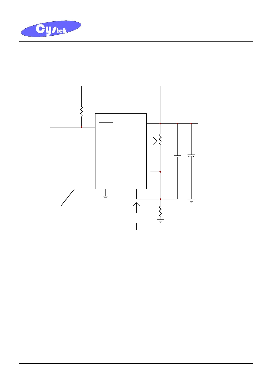
Block Diagram and Typical Applications
CAP
60mV
FEEDBACK
INPUT
OUTPUT
SENSE
XX V TAP
ERROR
GROUND
SHUTDOWN
TO CMOS
OR TTL
Vo=XX V
100mA Max
1.23V
REF
ERROR AMPLIFIER
4
5
6
2
1
8
7
3
CYStech Electronics Corp.
Spec. No. : C503Q8
Issued Date : 2003.03.21
Revised Date :
Page No. : 4/5
PL2951Q8
CYStek Product Specification
+
V
IN
SHUTDOWN INPUT 3
SD
GND
4
FB
VREF
7
1.23V
R2
3.3F
0.01µF
R1
V
OUT
1
V
OUT
1.2V to 30V
ERROR
ERROR OUTPUT
100k
5
ON
OFF
NOTE:PINS 2 AND 6 ARE LEFT OPEN
VOUT=VREF (1+R1/R2)
+V
IN
8

CYStech Electronics Corp.
Spec. No. : C503Q8
Issued Date : 2003.03.21
Revised Date :
Page No. : 5/5
PL2951Q8
CYStek Product Specification
SO-8 Dimension
*: Typical
Inches Millimeters
Inches Millimeters
DIM
Min. Max. Min. Max.
DIM
Min. Max. Min. Max.
A 0.1909
0.2007 4.85 5.10 I 0.0019
0.0078 0.05 0.20
B 0.1515
0.1555 3.85 3.95 J 0.0118
0.0275 0.30 0.70
C 0.2283
0.2441 5.80 6.20 K 0.0074
0.0098 0.19 0.25
D 0.0480
0.0519 1.22 1.32 L 0.0145
0.0204 0.37 0.52
E 0.0145
0.0185 0.37 0.47 M 0.0118
0.0197 0.30 0.50
F 0.1472
0.1527 3.74 3.88 N 0.0031
0.0051 0.08 0.13
G 0.0570
0.0649 1.45 1.65 O 0.0000
0.0059 0.00 0.15
H
0.1889
0.2007
4.80
5.10
Notes:
1.Controlling dimension: millimeters.
2.Maximum lead thickness includes lead finish thickness, and minimum lead thickness is the minimum thickness of base material.
3.If there is any question with packing specification or packing method, please contact your local CYStek sales office.
Material:
∑
Lead: 42 Alloy; solder plating
∑
Mold Compound: Epoxy resin family, flammability solid burning class: UL94V-0
Important Notice:
∑
All rights are reserved. Reproduction in whole or in part is prohibited without the prior written approval of CYStek.
∑
CYStek reserves the right to make changes to its products without notice.
∑
CYStek semiconductor products are not warranted to be suitable for use in Life-Support Applications, or systems.
∑
CYStek assumes no liability for any consequence of customer product design, infringement of patents, or application assistance.
8-Lead SO-8 Plastic Package
CYStek Package Code: S8
Marking:
Top View
A
B
Front View
F
C
D
E
G
Part A
I
H
J
K
O
M
L
N
Right side View
Part A
2951