
CYStech Electronics Corp.
Spec. No. : C501Q8
Issued Date : 2003.03.21
Revised Date :
Page No. : 1/7
PL34063AQ8
CYStek Product Specification
DC-to-DC Converter Control Circuit
PL34063AQ8
Description
The PL34063AQ8 is a monolithic control circuit containing the primary functions required for
DC-to-DC converters. This device consists of an internal temperature compensated reference,
comparator, control- led duty cycle oscillator with an active current limit circuit, driver and high current
output switch.
Features
∑
3V to 40V Input Voltage Operation
∑
Internal 1.6A Peak Current Switch
∑
Internal ±1.8% Reference
∑
Low Quiescent Current at 1.6mA
∑
Frequency Operation from 100Hz~100KHz
∑
Current Limiting
Applications
∑
Saver for Cellular Phone
∑
DC-DC Converter Module
Typical Application Circuit
1
8
2
3
4
5
6
7
Fig1.Saver Circuit for Cellular Phone
V
in
V
out
C
out
220
µ
F
D1
1N5819
C
T
470
F
RSC
C1
100
µ
F
RA
5.6k
RB
33k
200
µ
H
L1
PL34063A

CYStech Electronics Corp.
Spec. No. : C501Q8
Issued Date : 2003.03.21
Revised Date :
Page No. : 2/7
PL34063AQ8
CYStek Product Specification
Pin Connections
Pin1:Switch Collector
Pin5:Comparator Inverting Input
Pin2:Switch Emitter
Pin6:Vcc
Pin3:Timing Capacitor
Pin7:Ipk Sense
1
2
3
4
5
6
7
8
Pin4:Gnd Pin8:Driver
Collector
Absolute Maxium Rating
Supply Voltage ....................................................................................................................................... 40 V
Comparator Input Voltage Range ........................................................................................... -0.3 V ~ 40 V
Switch Collector Voltage ....................................................................................................................... 40 V
Switch Emitter Voltage .......................................................................................................................... 40 V
Switch Collector to Emitter Voltage ...................................................................................................... 40 V
Driver Collector Voltage ........................................................................................................................ 40 V
Switch Current ....................................................................................................................................... 1.6A
Power Dissipation DIP Package Ta=25
∞
C........................................................................................ 625 mW
Thermal Resistance Junction to Air............................................................................................. 160
∞
C / W
Operating Junction Temperature......................................................................................................... 125
∞
C
Operating Ambient Temperature Range......................................................................................... 0 ~ 70
∞
C
Storage Temperature Range.................................................................................................. -40
∞
C ~ 125
∞
C
Electrical Characteristics
(Vcc=5V,Ta=25
∞
C, unless otherwise specified)
Parameter Test
Condition
Symbol
Min.
Typ.
Max.
Unit
Oscillator
Charging Current
5.0V
V
CC
40V
I
chg
24
35
42
uA
Discharge Current
5.0V
V
CC
40V
I
dischg
140
220
260
uA
Voltage Amplitude
Pin3
V
OSC
-
0.6
-
V
Discharge to Charge Current Ratio
V
IPK(Sense)
=V
CC
I
Dischg
/I
chg
5.2 6.5 7.5
Current Limit Sense Voltage
I
Chg
=I
dischg
V
IPK(Sence)
250 300 350 mV
Output Switch
Saturation Voltage, Darlington
Connection
I
SW
=1.0A,
V
C(Driver)=
VC(Switch)
V
CE(Sat)
-
1.0
1.3
V
Saturation Voltage
I
SW
=1.0A, I
C(Driver)
=50mA
(Forced
20)
V
CE(Sat)
-
0.4
0.7
V
DC Current Gain
I
SW
=1.0A, V
CE
=5.0V hFE
50
75
-
V
Collector Off-State Current
V
CE
=40V I
CC(Off)
-
0.01
100
uA
Comparator
Threshold Voltage
Threshold Voltage
0
∞
C
Ta
70
∞
C
V
FB
1.227
1.210
1.250
-
1.273
1.29
V
Threshold Voltage Line Regulation
3.0V
V
CC
40V
Regline -
1.5
6
mV
Input Bias Current
V
IN
=0V I
IB
-
-20
-400
nA
Supply Current
V
IPK(Sence)
=V
CC
V
Pin5
>
V
FB
,
5.0V
V
CC
40V
C
T
=0.0001uF,Pin2=Gnd
Remaining pins open
I
CC
-
1.6
3
mA

CYStech Electronics Corp.
Spec. No. : C501Q8
Issued Date : 2003.03.21
Revised Date :
Page No. : 3/7
PL34063AQ8
CYStek Product Specification
Block Diagram
Application Information
Design Formula Table
Calculation Step-Down
Step-Up
Voltage-Inverting
t
on
/ t
off
V
out
+V
F
/
V
in(min)
-V
sat
-V
Out
Vout+V
F
-V
in(min)
/
V
in(min)
-V
sat
|V
out
| + V
F /
V
in
-V
sat
(t
on
+ t
off
) max
1/F
min
1/F
min
1/F
min
C
T
4*10
-5
t
on
4*10
-5
t
on
4*10
-5
t
on
I
C(switch)
2*I
out(max)
2*I
out(max)
(t
on
+t
off
/t
off
)
2*I
out(max)
(t
on
+t
off
/t
off
)
RS
0.3 / I
C(switch)
0.3 / I
C(switch)
0.3 / I
C(switch)
L
(min)
(V
in(min)-
V
sat
-V
out
/
I
C(switch)
)
*t
on(max)
(V
in(min)-
V
sat
/
I
C(switch)
)
*t
on(max)
(V
in(min)-
V
sat
/
I
C(switch)
)
*t
on(max)
C
O
I
C(switch)
*(t
on
+t
off)
/
8V
Ripple(P-P)
I
out
*t
on
/ V
Ripple(P-P)
I
out
*t
on
/ V
Ripple(P-P)
V
sat
: Saturation voltage of the output switch.
V
F
: Forward voltage drop of the ringback rectifier.
The following power supply characteristics must be chosen :
V
in
: Nominal input voltage.
V
out
: Desired output voltage. |V
out
|=1.25*(1+RB/RA)
I
out
- Desired output current
Fmin : Minimum desired output switching frequency at the selected values for V
in
and I
out
.
V
Ripple(P-P)
: Desired peak to peak output ripple voltage in practice, the calculated value will need to be increased
due to the capacitor equivalent series resistance and board layout. The ripple voltage should be kept to a low value
since it will directly effect the line and load regulation.
SC
Pin1:1.6A Switch Collector
TC
Pin3:Oscilletor Timing Capacitor
GND
Pin4:Power GND
DRI
Pin8:Driver Collector
IPK
Pin7:Highside Current Sense
Input, VCC-VIPK=300mV
VCC
Pin6:Power Supply Input
FB
Pin5:Feedback Comparator
Inverting Input
SE
Pin2:Darlington Switch Emitter
Q1
Q2
80
Q S
R
CT
IPK
Oscillator
Comparator
1.25V
Reference Voltage
+
-

CYStech Electronics Corp.
Spec. No. : C501Q8
Issued Date : 2003.03.21
Revised Date :
Page No. : 4/7
PL34063AQ8
CYStek Product Specification
Application Information
(Continued)
1
8
2
3
4
5
6
7
V
out
28V / 200mA
R1
150
C
out
220
µ
F
C
T
680
F
V
in
RA
2.2k
RSC
0.22
C1
100
µ
F
PL34063A
L1
D1
200
µ
H
1N5819
RB
47k
Line Regulation : 100mV (V
in
=8V~16V, @I
o
=200mA)
Load Regulation : 5mV (Vin=12V, @Io=80mA~200mA)
Fig.2 Step-Up Converter
1
8
2
3
4
5
6
7
PL34063A
RSC
C1
RA
R1
RB
C
T
D1
L1
Q1
R2
V
in
V
out
C
out
Fig.3 Step-Up Converter With External NPN Switch
1
8
2
3
4
5
6
7
Fig.4 Step-Down Converter
Line Regulation : 40mV (V
in
=10V~20V, @I
o
=500mA)
Load Regulation : 5mV (Vin=15V, @Io=10mA~500mA)
Short Circuit Current : 1.3A (Vin=15V, @RL=0.1
)
PL34063A
V
out
5V / 500mA
RSC
0.25
L1
RB
RA
1.2k
3.6k
C
T
470
F
D1
1N5819
200
µ
H
C
out
470
µ
F
C1
100
µ
F
V
in
CYStech Electronics Corp.
Spec. No. : C501Q8
Issued Date : 2003.03.21
Revised Date :
Page No. : 5/7
PL34063AQ8
CYStek Product Specification
Application Information
(Continued)
V
in
1
8
2
3
4
5
6
7
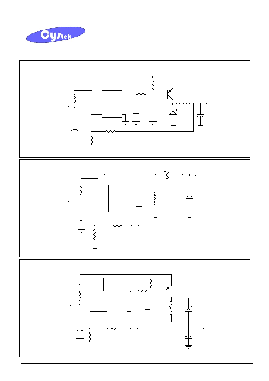
Fig.5 Step-Down Converter With External PNP Saturation Switch
V
out
PL34063A
R2
R1
Q1
L1
D1
RSC
C1
RA
RB
C
out
C
T
1
8
2
3
4
5
6
7
Fig.6 Voltage Inverting Converter
V
out
-12V / 100mA
C
out
470
µ
F
L1
100
µ
H
D1
1N5819
C
T
680
F
PL34063A
RSC
0.25
C1
100
µ
F
RB
8.2k
RA
953
V
in
4.5V-6V
Line Regulation : 20mV (V
in
=4.5V~6V, @I
o
=100mA)
Load Regulation : 100mV (Vin=5V, @Io=10mA~100mA)
1
8
2
3
4
5
6
7
Fig.7 Voltage Inverting Converter With External PNP Saturation Switch
V
out
C
out
D1
L1
R1
R2
PL34063A
C
T
RSC
RA
RB
C1
V
in
Q1

CYStech Electronics Corp.
Spec. No. : C501Q8
Issued Date : 2003.03.21
Revised Date :
Page No. : 6/7
PL34063AQ8
CYStek Product Specification
Characteristic Curves
Output Switch On-Off Time vs Oscillator
Timing Capacitance
1
10
100
1000
0.01
0.1
1
10
Oscillator Timing Capacitance---CT(nF)
Output Switch On-Off Time---ton-off(
us
ton
toff
V
CC
=5.0V
Pin 7=V
CC
Pin 5=GND
T
A
=25
Emitter Follower Configuration Output
Saturation Voltage vs Emitter Current
1
1.1
1.2
1.3
1.4
1.5
1.6
1.7
1.8
0
0.2
0.4
0.6
0.8
1
1.2
1.4
1.6
Emitter Current---IE(A)
Saturation Voltage---VCE(sat)(
V)
V
CC
=5V
Pins 1,7,8=V
CC
Pins 3,5=Gnd
T
A
=25
(See Note )
Common Emitter Configuration Output Switch
Saturation Voltage vs Collector Current
0
0.1
0.2
0.3
0.4
0.5
0.6
0.7
0.8
0.9
1
1.1
0
0.2
0.4
0.6
0.8
1
1.2
1.4
1.6
Collector Current---IC(A)
Saturation Voltage---V
CE(sat)
(V)
Darlington Connection
Forced =20
VCC=5V
Pin 7=VCC
Pins 2,3,5=Gnd
TA=25
(See Note)
Current Limit Sense Voltage vs Temperature
200
220
240
260
280
300
320
340
360
380
400
-75
-50
-25
0
25
50
75
100 125
Ambient Temperature---TA()
Current Limit Sense Voltage---VIPK(
V)
V
CC
=5.0V
Ichg=Idischg
Standby Supply Current vs Supply Voltage
0
0.4
0.8
1.2
1.6
2
2.4
2.8
3.2
3.6
0
5
10
15
20
25
30
35
40
Supply Voltage---VCC(V)
Supply Current---I
CC
(mA)
C
T
=10nF
Pin 7=V
CC
Pin 2=Gnd
Note: Low duty cycle pulse techniques are used during test
to maintain junction temperature as close to ambient
temperature as possible.

CYStech Electronics Corp.
Spec. No. : C501Q8
Issued Date : 2003.03.21
Revised Date :
Page No. : 7/7
PL34063AQ8
CYStek Product Specification
SO-8 Dimension
*: Typical
Inches Millimeters
Inches Millimeters
DIM
Min. Max. Min. Max.
DIM
Min. Max. Min. Max.
A 0.1909
0.2007 4.85 5.10 I 0.0019
0.0078 0.05 0.20
B 0.1515
0.1555 3.85 3.95 J 0.0118
0.0275 0.30 0.70
C 0.2283
0.2441 5.80 6.20 K 0.0074
0.0098 0.19 0.25
D 0.0480
0.0519 1.22 1.32 L 0.0145
0.0204 0.37 0.52
E 0.0145
0.0185 0.37 0.47 M 0.0118
0.0197 0.30 0.50
F 0.1472
0.1527 3.74 3.88 N 0.0031
0.0051 0.08 0.13
G 0.0570
0.0649 1.45 1.65 O 0.0000
0.0059 0.00 0.15
H
0.1889
0.2007
4.80
5.10
Notes:
1.Controlling dimension: millimeters.
2.Maximum lead thickness includes lead finish thickness, and minimum lead thickness is the minimum thickness of base material.
3.If there is any question with packing specification or packing method, please contact your local CYStek sales office.
Material:
∑
Lead: 42 Alloy; solder plating
∑
Mold Compound: Epoxy resin family, flammability solid burning class: UL94V-0
Important Notice:
∑
All rights are reserved. Reproduction in whole or in part is prohibited without the prior written approval of CYStek.
∑
CYStek reserves the right to make changes to its products without notice.
∑
CYStek semiconductor products are not warranted to be suitable for use in Life-Support Applications, or systems.
∑
CYStek assumes no liability for any consequence of customer product design, infringement of patents, or application assistance.
8-Lead SO-8 Plastic Package
CYStek Package Code: Q8
Marking:
Top View
A
B
Front View
F
C
D
E
G
Part A
I
H
J
K
O
M
L
N
Right side View
Part A
34063A