 | –≠–ª–µ–∫—Ç—Ä–æ–Ω–Ω—ã–π –∫–æ–º–ø–æ–Ω–µ–Ω—Ç: PL432DN3 | –°–∫–∞—á–∞—Ç—å:  PDF PDF  ZIP ZIP |

cys
tek
CYStech Electronics Corp.
Spec. No. : C504A3
Issued Date : 2003.03.21
Revised Date :
Page No. : 1/9
PL432XA3/N3
CYStek Product Specification
Adjustable shunt regulator
PL432XA3/N3
Description Features
The PL432 is a three terminal adjustable shunt Low voltage operation(down to 1.24V)
regulator with thermal stability guaranteed over Wide operating current range 80A to 100mA
temperature. The output voltage can be adjusted Low dynamic output impedance 0.05 typ.
to any value from 1.24V(V
REF
) to 20V with two Trimmed bandgap design ±0.25%
external resistors. The PL432 has a typical dynamic Upgrade for PL431
output impedance of 0.05. Active output circuitry Available in TO-92 and SOT-23 packages
provides a very sharp turn on characteristic, making
the PL432 an excellent replacement for zener diodes.
Applications
The PL432 shunt regulator is available with four Linear Regulators
Voltage tolerances(0.25%,0.5%,1% and 2%), and two Adjustable Supplies
package options(TO-92 and SOT-23). This allows the Switching Power Supplies
designer the opportunity to select the optimum combi- Battery Operated Computers
nation of cost and performance for their application. Instrumentation
Computer Disk Drives
Typical Application Circuit
(Note 1,2)
Notes:
1) Set V
OUT
according to the following equation:
V
OUT
=V
REF
(1+R1/R2)+I
REF
R1
2) Choose the value for R as follows:
The maximum limit for R should be such that the
cathode current, Iz, is greater than the minimum
operating current(80A) at VI
N(MIN)
.
The minimum limit for R should be as such that Iz
does not exceed 100mA under all load conditions,
and the instantaneous turn-on value for Iz does not
exceed 150mA. Both of the following conditions
must be met:
Rmin
V
IN(max)
/150mA(to limit instantaneous
turn-on Iz)
Rmin
V
IN(max)
-V
OUT
(to limit Iz under
I
OUT(min)
+100mA normal operating
conditions)
VIN
GND
R
R1
R2
VREF
PL432
VOUT

cys
tek
CYStech Electronics Corp.
Spec. No. : C504A3
Issued Date : 2003.03.21
Revised Date :
Page No. : 2/9
PL432XA3/N3
CYStek Product Specification
Absolute Maximum Ratings
Parameter
Symbol
Maximum
Units
Cathode Voltage
Vz
20
V
Continuous Cathode Current
I
Z
100
mA
Reference Input Current
I
REF
3
mA
Power Dissipation at T
A
=25
SOT-23
TO-92
P
D
0. 37
0.95
W
Thermal Resistance
SOT-23
TO-92
JA
336
132
/W
Operating Ambient Temperature Range
T
A
0 to +70
Operating Junction Temperature Range
T
J
0 to +150
Storage Temperature Range
Tstg
-65 to +150
Lead Temperature(Soldering) 10 seconds
T
LEAD
300
ESD Rating(Human Body Model)
V
ESD
2
kV
Electrical Characteristics
Unless otherwise specified, TA=25. Values in bold apply over full operating ambient temperature range.
PL432D PL432C
Parameter Symbol
Condition Min
Typ
Max
Min
Typ
Max
Unit
Reference Voltage
V
REF
V
Z
=V
REF
,I
Z
=10mA(Note 1)
1.237
1.224
1.240
1.243
1.256
1.234
1.222
1.240 1.246
1.258
V
V
REF
Temperature
Deviation
V
DEV
V
Z
=V
REF
,I
Z
=10mA(Note 1)
-
10 25 -
10 25 mV
Ratio of Change in
V
REF
to change in V
Z
V
REF
V
Z
I
Z
=10mA, V
Z
=16V to V
REF
- -1.0
-2.7 - -1.0
-2.7
mV/V
Reference Input
Current
I
REF
R1=10k,R2=,
I
Z
=10mA(Note2)
- 0.15 0.5 - 0.15
0.5 A
I
REF
Temperature
Deviation
I
REF(DEV)
R1=10k,R2=,
I
Z
=10mA(Note 2)
-
0.1 0.4 -
0.1 0.4 A
V
REF
=0V,V
Z
=6V(Note
3)
- 0.125
0.150 - 0.125
0.150
Off-state Cathode
Current
I
Z(OFF)
V
REF
=0V,V
Z
=16V(Note
3)
- 0.135
0.150 - 0.135
0.150
A
Dynamic Output
Impedance
r
z
f <1kHz,V
Z
=V
REF
I
Z
=100A to 100mA(Note 1)
- 0.05
0.15 - 0.05
0.15
Minimum Operating
Current
I
Z(MIN)
V
Z
=V
REF
(Note 1)
-
20
80
- 20 80
A

cys
tek
CYStech Electronics Corp.
Spec. No. : C504A3
Issued Date : 2003.03.21
Revised Date :
Page No. : 3/9
PL432XA3/N3
CYStek Product Specification
Electrical Characteristics(Cont.)
Unless otherwise specified, TA=25. Values in bold apply over full operating ambient temperature range.
PL432B PL432A
Parameter Symbol
Condition Min
Typ
Max
Min
Typ
Max
Unit
Reference Voltage
V
REF
V
Z
=V
REF
,I
Z
=10mA(Note 1)
1.228
1.215
1.240
1.252
1.265
1.215
1.200
1.240 1.265
1.280
V
V
REF
Temperature
Deviation
V
DEV
V
Z
=V
REF
,I
Z
=10mA(Note 1)
-
10 25 -
10 35 mV
Ratio of Change in
V
REF
to change in V
Z
V
REF
V
Z
I
Z
=10mA, V
Z
=16V to V
REF
- -1.0
-2.7 - -1.0
-2.7
mV/V
Reference Input
Current
I
REF
R1=10k,R2=,
I
Z
=10mA(Note2)
- 0.15 0.5 - 0.15
0.5 A
I
REF
Temperature
Deviation
I
REF(DEV)
R1=10k,R2=,
I
Z
=10mA(Note 2)
-
0.1 0.4 -
0.1 0.4 A
V
REF
=0V,V
Z
=6V(Note
3)
- 0.125
0.150 - 0.125
0.150
Off-state Cathode
Current
I
Z(OFF)
V
REF
=0V,V
Z
=16V(Note
3)
- 0.135
0.150 - 0.135
0.150
A
Dynamic Output
Impedance
r
z
f<1kHz,V
Z
=V
REF
I
Z
=100A to 100mA(Note 1)
- 0.05
0.15 - 0.05
0.15
Minimum Operating
Current
I
Z(MIN)
V
Z
=V
REF
(Note 1)
-
20
80
- 20 80
A
Notes:
(1) See Test Circuit 1.
(2) See Test Circuit 2.
(3) See Test Circuit 3.
Recommended Operating Conditions
Symbol Min Max Unit
Cathode Voltage
V
Z
V
REF
16
V
Cathode Current
I
Z
0.08 100
mA
Test Circuits
VIN
IREF
IZ
VZ
Test Circuit 1
VZ=VREF
VIN
VZ
IZ
IREF
R1
R2
VREF
Test Circuit 2
VZ>VREF
VIN
VZ
IZ(off)
Test Circuit 3
Off-State
cys
tek
CYStech Electronics Corp.
Spec. No. : C504A3
Issued Date : 2003.03.21
Revised Date :
Page No. : 4/9
PL432XA3/N3
CYStek Product Specification
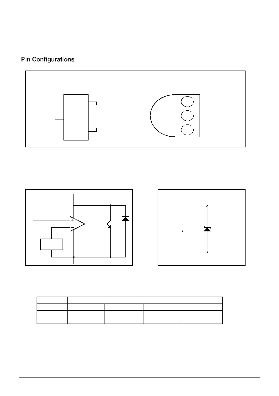
Cathode
Reference
Anode
3
2
1
3
2
1
Cathode
Anode
Reference
TO-92(Top View)
SOT-23(Top View)
Block Diagram Symbol
REF
Anode
Cathode
Ordering Information
Package
Tolerance
0.25%
0.5%
1%
2%
TO-92
PL432DA3
PL432CA3
PL432BA3
PL432AA3
SOT-23
PL432DN3
PL432CN3
PL432BN3
PL432AN3
VREF
Anode
REF
Cathode

cys
tek
CYStech Electronics Corp.
Spec. No. : C504A3
Issued Date : 2003.03.21
Revised Date :
Page No. : 5/9
PL432XA3/N3
CYStek Product Specification
Characteristic Curves
Cathode Current vs Cathode Voltage
-300
-200
-100
0
100
200
300
-1
-0.5
0
0.5
1
1.5
Cathode Voltage---Vz(V)
Cathode Current---IZ(
A)
Vz=V
REF
TA=25
Cathode Current vs Cathode Voltage
-150
-100
-50
0
50
100
150
-1.5
-1
-0.5
0
0.5
1
1.5
Cathode Voltage---Vz(V)
Cathode Current---Iz(m
A)
Vz=VREF
TA=25
Reference Voltage vs Junction Temperature
1.234
1.236
1.238
1.24
1.242
1.244
1.246
1.248
-50
0
50
100
150
Junction Temperature---TJ()
Reference Voltage---VREF(
V)
IZ=60A
Iz=10mA
Reference Input Current vs Junction Temperature
50
75
100
125
150
-50
-25
0
25
50
75
100
125
150
Junction Temperature---TJ()
Reference Input Current---IREF(n
A)
Iz=10mA
R1=10k
R2=
Ratio of Delta Reference Voltage to Delta Cathode
Voltage vs Junction Temperature
0
0.1
0.2
0.3
0.4
0.5
0.6
0.7
0.8
0.9
1
1.1
1.2
-50
-25
0
25
50
75
100
125
150
Junction Temperature---TJ()
VREF/Vz---(-mV/
V)
Iz=10mA
Vz=16V to VREF
Off-State Cathode Current
vs Junction Temperature
0
50
100
150
200
250
-50
-25
0
25
50
75
100
125
150
Junction Temperature---TJ()
Off-State Cathode Current---
Iz
(off)(nA)
V
REF
=0V
Vz=16V
Vz=6V

cys
tek
CYStech Electronics Corp.
Spec. No. : C504A3
Issued Date : 2003.03.21
Revised Date :
Page No. : 6/9
PL432XA3/N3
CYStek Product Specification
Reference Impedance vs Junction Temperature
0
0.05
0.1
0.15
0.2
0.25
0.3
0.35
0.4
0.45
0.5
-50
-25
0
25
50
75
100
125 150
Junction Temperature---TJ()
Reference Impedance---rz()
Iz=0.1 to 100mA
Vz=V
REF
f<1kHz
Reference Impedance vs Frequency
0.1
1
10
100
1000
10000
100000
1000000
Frequency---f(Hz)
Reference Impedance---rz()
T
A
=25
Small-Signal Gain vs Frequency
-20
-10
0
10
20
30
40
50
60
70
100
1000
10000
100000
1000000
Frequency---f(Hz)
Small-Signal Gain---AV(d
B)
Small-Signal Phase Shift vs Frequency
-360
-315
-270
-225
-180
100
1000
10000
100000
1000000
Frequency---f(Hz)
Small-Signal Phase Shift---(Deg)
Stability Boundary Condition For Shunt Regulation
vs Cathode Current and Load Capacitance
0
0.5
1
1.5
2
2.5
3
3.5
0.001
0.01
0.1
1
10
Load Capacitance---CL(F)
Cathode Current---Iz(m
A)
T
A
=25
Stable
Stable
Vz=V
REF
Vz=2V

cys
tek
CYStech Electronics Corp.
Spec. No. : C504A3
Issued Date : 2003.03.21
Revised Date :
Page No. : 7/9
PL432XA3/N3
CYStek Product Specification
Test Circuit-Small-Signal Gain and Phase
Test Circuit-Stability
+
15k
8.25k
PL432
232
Iz
OUT
GND
10F
Applications Information - Stability
Selection of load capacitance when using PL432 as a shunt regulator
When the PL432 is used as a shunt regulator, two options for selection of C
L
(see diagram on page 6)
are recommended for optimal stability:
1) No load capacitance across the device, decouple at the load.
2) Large capacitance across the device, optimal decoupling at the load.
The reason for this is that PL432 exhibits instability with capacitances in the range of 10nF to 1F
(approx.) at light cathode currents(up to 3mA typical). The device is less stable the lower the cathode
voltage has been set for. Therefore while the device will be perfectly stable operating at a cathode
current of (say) 10mA with a 0.1F capacitor across it, it will oscillate transiently during start-up as the
cathode current passes through the instability region. Selecting a very low (or preferably, no) capaci-
tance, or alternatively a high capacitance(such as 10F) will avoid this issue altogether. Since the user
will probably wish to have local decoupling at the load anyway, the most cost effective method is to use
no capacitance at all directly across the device. PCB trace/via resistance and inductance prevent the
local load decoupling from causing the oscillation during the transient start-up phase.
Note : if the PL432 is located right at the load, so the load decoupling capacitor is directly across it, then
this capacitor will have to be 1nF or 10F.
Iz
R1
R2
PL432
R
CL

cys
tek
CYStech Electronics Corp.
Spec. No. : C504A3
Issued Date : 2003.03.21
Revised Date :
Page No. : 8/9
PL432XA3/N3
CYStek Product Specification
TO-92 Dimension
*: Typical
Inches Millimeters
Inches Millimeters
DIM
Min. Max. Min. Max.
DIM
Min. Max. Min. Max.
A 0.1704
0.1902 4.33 4.83 G 0.0142 0.0220 0.36 0.56
B 0.1704
0.1902 4.33 4.83 H
-
*
0.1000 -
*
2.54
C 0.5000 - 12.70 -
I
-
*
0.0500 -
*
1.27
D 0.0142
0.0220 0.36 0.56
1
-
*
5
∞
-
*
5
∞
E -
*
0.0500 -
*
1.27
2
-
*
2
∞
-
*
2
∞
F 0.1323
0.1480 3.36 3.76
3
-
*
2
∞
-
*
2
∞
Notes:
1.Controlling dimension: millimeters.
2.Maximum lead thickness includes lead finish thickness, and minimum lead thickness is the minimum thickness of base material.
3.If there is any question with packing specification or packing method, please contact your local CYStek sales office.
Material:
∑
Lead: 42 Alloy ; solder plating
∑
Mold Compound: Epoxy resin family, flammability solid burning class: UL94V-0
C
PL431
3-Lead TO-92 Plastic Package
CYStek Package Code: A3
Marking:
3
1
A
D
B
C
I
1
E
F
2
3
G
H
2
Style: Pin 1.Reference 2.Anode 3.Cathode
432

cys
tek
CYStech Electronics Corp.
Spec. No. : C504A3
Issued Date : 2003.03.21
Revised Date :
Page No. : 9/9
PL432XA3/N3
CYStek Product Specification
SOT-23 Dimension
*: Typical
Inches Millimeters
Inches Millimeters
DIM
Min. Max. Min. Max.
DIM
Min. Max. Min. Max.
A 0.1102
0.1204 2.80 3.04 J 0.0034
0.0070
0.085 0.177
B 0.0472
0.0630 1.20 1.60 K 0.0128 0.0266 0.32 0.67
C 0.0335
0.0512 0.89 1.30 L 0.0335 0.0453 0.85 1.15
D 0.0118
0.0197 0.30 0.50 S 0.0830
0.1083 2.10 2.75
G 0.0669
0.0910 1.70 2.30 V 0.0098 0.0256 0.25 0.65
H
0.0005
0.0040
0.013
0.10
Notes:
1.Controlling dimension: millimeters.
2.Maximum lead thickness includes lead finish thickness, and minimum lead thickness is the minimum thickness of base material.
3.If there is any question with packing specification or packing method, please contact your local CYCtek sales office.
Material:
∑
Lead: 42 Alloy; solder plating
∑
Mold Compound: Epoxy resin family, flammability solid burning class: UL94V-0
Important Notice:
∑
All rights are reserved. Reproduction in whole or in part is prohibited without the prior written approval of CYStek.
∑
CYStek reserves the right to make changes to its products without notice.
∑
CYStek semiconductor products are not warranted to be suitable for use in Life-Support Applications, or systems.
∑
CYStek assumes no liability for any consequence of customer product design, infringement of patents, or application assistance.
H
J
K
D
A
L
G
V
C
B
3
2
1
S
Style: Pin 1.Reference 2.Cathode
3.Anode
3-Lead SOT-23 Plastic
Surface Mounted Package
CYStek Package Code: N3
Marking:
432