 | –≠–ª–µ–∫—Ç—Ä–æ–Ω–Ω—ã–π –∫–æ–º–ø–æ–Ω–µ–Ω—Ç: PL7808XE3 | –°–∫–∞—á–∞—Ç—å:  PDF PDF  ZIP ZIP |
CYStech Electronics Corp.
Spec. No. : C523E3
Issued Date : 2003.04.02
Revised Date :
Page No. : 1/3
PL7808E3
CYStek Product Specification
3-TERMINAL POSITIVE VOLTAGE REGULATOR
PL7808XE3
Description
The PL7808XE3 series of three-terminal positive regulators are
available in the TO-220AB package. These regulators can provide
local on -card regulation, eliminating the distribution problems
associated with single point regulation. Each employs internal current
limiting, thermal shutdown and safe operating area protection, making it essentially indestructible.
If adequate heat sinking is provided, they can deliver over 1A output current. Although designed
primarily as fixed voltage regulators, these devices can be used with external components to
obtain adjustable voltages and currents.
PL7808XE3 is characterized for operation from 0
∞
C to +125
∞
C, and if operating temperature is
always high, please refer to the power dissipation curve.
Absolute Maximum Ratings
(Ta=25
∞
C)
∑
Input Voltage ....................................................................................................................... 35 V
∑
Total Power Dissipation .................................................................................... Internally limited
∑
Operating Temperature Range .......................................................................... 0
∞
C to +125
∞
C
∑
Maximum Junction Temperature ..................................................................................... 125
∞
C
∑
Storage Temperature Range .......................................................................... -55
∞
C to +150
∞
C
∑
Lead Temperature (Soldering 10S) ................................................................................. 230
∞
C
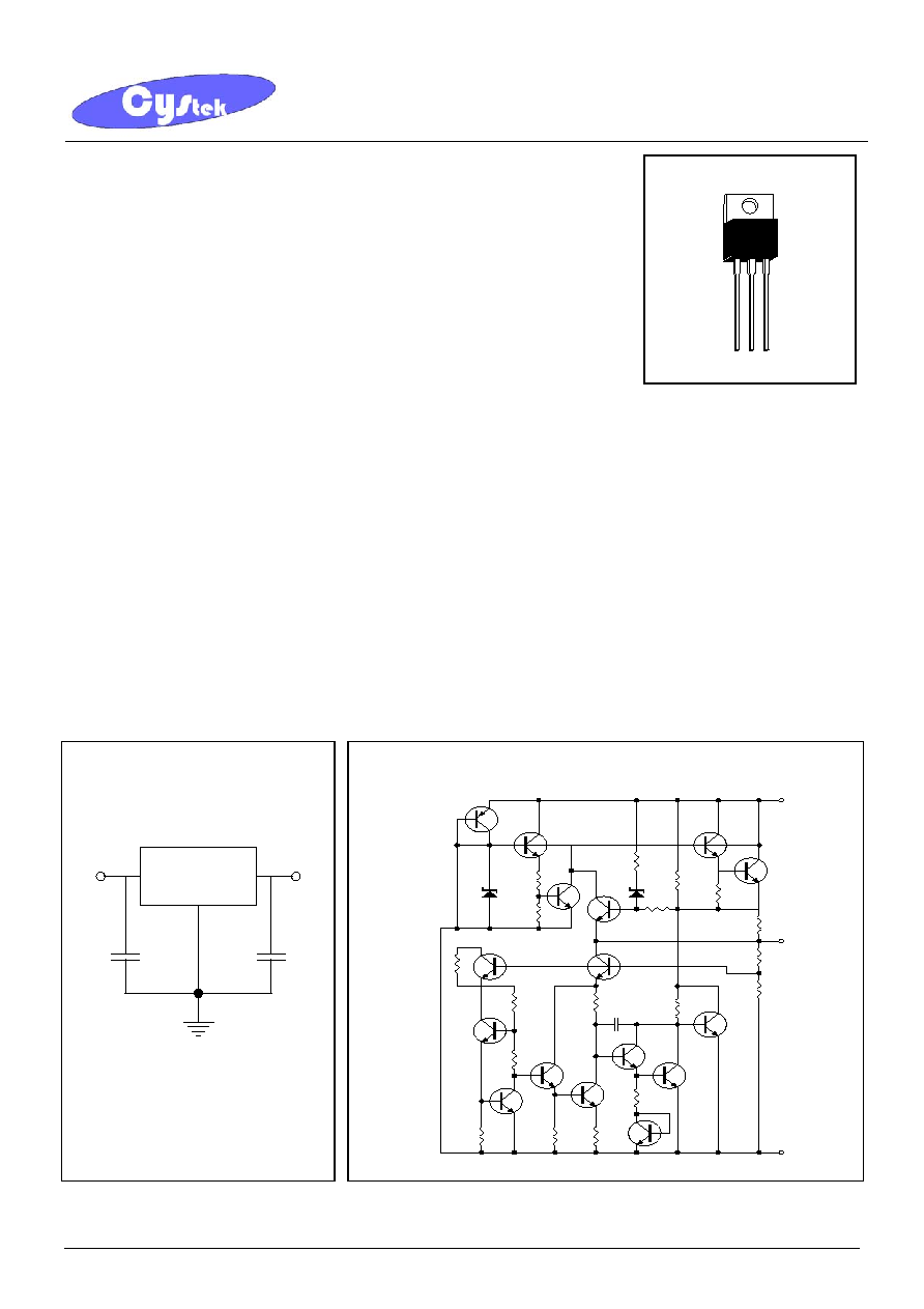
Typical Application
Schematic Diagram
6.3V
3.4K
200
10K
200
1K
2K
0.3
26
4K
20pF
4K
1K
12.1K
1.2
26
1.9K
30K
VREF
Input
Output
GND
PL7808
Vout
Vin
3
1
2
C1 C2
Note:
C1 and C2 are required if regulator is
located far from power supply filter
and load, or oscillation may induced
on the loop.
TO-220AB

CYStech Electronics Corp.
Spec. No. : C523E3
Issued Date : 2003.04.02
Revised Date :
Page No. : 2/3
PL7808E3
CYStek Product Specification
Electrical Characteristics
Vin=14V, Io=500mA, 0
∞
C
Tj
125
∞
C (unless otherwise noted)
PL7808A
Symbol Parameter
Conditions
Min Typ Max
Units
Tj=25
∞
C
7.76 8 8.24
Vo Output
Voltage
PD
15W, 5mA
Io
1A
7.76 8 8.24
V
Tj=25
∞
C, 10.5V
Vin
25V
- 5 80
Vo
Line Regulation
Tj=25
∞
C, 11.5V
Vin
17V
- 5 40
mV
5mA
Io
1.5A
- -
100
Vo
Load Regulation
250mA
Io
750mA
- - 50
mV
IQ Quiescent
Current Io
1A, Tj=25
∞
C
- 5.5 8 mA
5mA
Io
1A
- - 0.5
IQ
Quiescent Current
Change
10.5V
Vin
25V
- - 1.3
mA
Vn
Output Noise Voltage Ta=25
∞
C, 10Hz
f
100KHz
- -
200
uV
RR Ripple
Rejection 11.5V
Vin
21.5V, f=120Hz
- 68 - dB
VD Dropout
Voltage Tj=25
∞
C, Io=1A
- 2 - V
Isc
Short Circuit Current Tj=25
∞
C
- 1.5 - A
Ipk
Peak Output Current Tj=25
∞
C
1.7 - - A
Vo /
T
Average Tc of Vout
0
∞
C
Tj
+125
∞
C, Io=5mA
- -0.8 - mV/
∞
C
PL7808B
Symbol Parameter
Conditions
Min Typ Max
Units
Tj=25
∞
C
7.7 8 8.3
Vo Output
Voltage
PD
15W, 5mA
Io
1A
7.6 8 8.4
V
Tj=25
∞
C, 10.5V
Vin
25V
- 5
160
Vo
Line Regulation
Tj=25
∞
C, 11.5V
Vin
17V
- 2 80
mV
5mA
Io
1.5A
- -
160
Vo
Load Regulation
250mA
Io
750mA
- - 80
mV
IQ Quiescent
Current Io
1A, Tj=25
∞
C
- 5.5 8 mA
5mA
Io
1A
- - 0.5
IQ
Quiescent Current
Change
10.5V
Vin
25V
- - 1.3
mA
Vn
Output Noise Voltage Ta=25
∞
C, 10Hz
f
100KHz
- -
300
uV
RR Ripple
Rejection 11.5V
Vin
21.5V, f=120Hz
62 73 - dB
VD Dropout
Voltage Tj=25
∞
C, Io=1A
- 2.5 - V
Isc
Short Circuit Current Tj=25
∞
C
- 1.5 - A
Ipk
Peak Output Current Tj=25
∞
C
1.7 - - A
Vo /
T
Average Tc of Vout
0
∞
C
Tj
+125
∞
C, Io=5mA
- -0.8 - mV/
∞
C

CYStech Electronics Corp.
Spec. No. : C523E3
Issued Date : 2003.04.02
Revised Date :
Page No. : 3/3
PL7808E3
CYStek Product Specification
TO-220AB Dimension
*: Typical
Inches Millimeters
Inches Millimeters
DIM
Min. Max. Min. Max.
DIM
Min. Max. Min. Max.
A 0.2197
0.2949 5.58 7.49 I
-
*
0.1508
-
*
3.83
B 0.3299
0.3504 8.38 8.90 K 0.0295 0.0374 0.75 0.95
C 0.1732 0.185 4.40 4.70 M 0.0449 0.0551 1.14 1.40
D 0.0453
0.0547 1.15 1.39 N
-
*
0.1000
-
*
2.54
E 0.0138
0.0236 0.35 0.60 O 0.5000
0.5618 12.70 14.27
G 0.3803
0.4047 9.66 10.28 P 0.5701
0.6248 14.48 15.87
H -
*
0.6398
-
*
16.25
Notes:
1.Controlling dimension: millimeters.
2.Maximum lead thickness includes lead finish thickness, and minimum lead thickness is the minimum thickness of base material.
3.If there is any question with packing specification or packing method, please contact your local CYStek sales office.
Material:
∑
Lead: 42 Alloy ; solder plating
∑
Mold Compound: Epoxy resin family, flammability solid burning class: UL94V-0
Important Notice:
∑
All rights are reserved. Reproduction in whole or in part is prohibited without the prior written approval of CYStek.
∑
CYStek reserves the right to make changes to its products without notice.
∑
CYStek semiconductor products are not warranted to be suitable for use in Life-Support Applications, or systems.
∑
CYStek assumes no liability for any consequence of customer product design, infringement of patents, or application assistance.
A
B
E
G
I
K
M
O
P
3
2
1
C
N
H
D
4
Style: Pin 1.Vin 2.Ground 3.Vout
4.Ground
3-Lead TO-220AB Plastic Package
CYStek Package Code: E3
Marking:
7808