Äîêóìåíòàöèÿ è îïèñàíèÿ www.docs.chipfind.ru
CYStech Electronics Corp.
Spec. No. : C520J3
Issued Date : 2003.04.10
Revised Date : . .
Page No. : 1/4
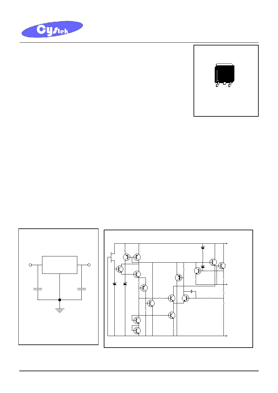
PL78M05J3
CYStek Product Specification
Three Terminal Medium Current Positive
Voltage Regulators
PL78M05XJ3
Description
These regulators employ internal current-limiting and thermal-shutdown,
making them essentially indestructible. They can deliver up to 500mA
output current, if the case temperature can be kept at Tc=25
°
C.
They are intended as fixed voltage regulators in a wide range of applications including local (on-card)
regulation for elimination of noise and distribution problems associated with single-point regulation. In
addition, they can be used with power pass elements to make high-current voltage regulators. The
PL78M05XJ3 used as a Zener diode/resistor combination replacement, offers an effective output
impedance improvement of typically two orders of magnitude, along with lower quiescent current and lower
noise.
Absolute Maximum Ratings
(Ta=25
°
C)
·
Input Voltage............................................................................................................. 35 V
·
Total Power Dissipation............................................................................... Internally limited
·
Operating Temperature Range...................................................................... 0
°
C to +125
°
C
·
Maximum Junction Temperature.................................................................................125
°
C
·
Storage Temperature Range........................................................................-55
°
C to +150
°
C
·
Lead Temperature (Soldering 10S)......................................
....................................260
°
C
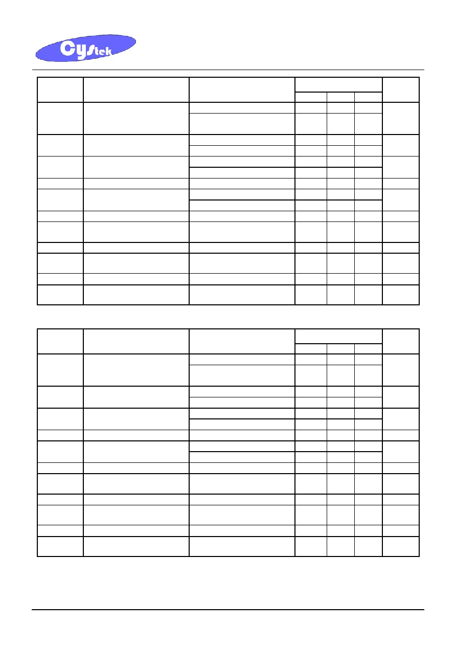
Schematic Diagram
Typical Application
TO-252
1.9k
Gnd
576
3.41k
3.89k
7.8k
13k
2.84k
5.7k
100
100
Vin
Vout
2.23k
1.5k
5k
5p
PL78M05
Vout
Vin
C1 C2
Note:
C1 and C2 are required if regulator is
located far from power supply filter
and load, or oscillation may induced
on the loop.
PL78M05
CYStech Electronics Corp.
Spec. No. : C520J3
Issued Date : 2003.04.10
Revised Date : . .
Page No. : 2/4
PL78M05J3
CYStek Product Specification
Ordering Information
Device
Output Voltage Range
PL78M05AJ3
4.8V4.9V
PL78M05BJ3
4.9V5.1V
PL78M05CJ3
5.1V5.2V
Electrical Characteristics
Vin=10V, Iout=350mA, P
D
5W,0
°
C
Tj
125
°
C, Cin=0.33uF, Cout=0.1uF (unless otherwise noted)
PL78M05A
Symbol Parameter
Conditions
Min Typ Max
Units
Tj=25
°
C
4.80 - 4.90
Vo Output
Voltage
5mA
Io
350mA and
7V
Vin
20V
4.75 - 5.25
V
Tj=25
°
C, 7V
Vin
25V
- 3
100
Vo
Line Regulation
Tj=25
°
C, 8V
Vin
25V
- -
50
mV
Tj=25
°
C, 5mA
Io
500mA
- 15
100
Vo
Load Regulation
Tj=25
°
C, 5mA
Io
200mA
- -
50
mV
IQ Quiescent
Current
Tj=25
°
C
- 3.2 6 mA
5mA
Io
350mA
- -
0.5
IQ
Quiescent Current
Change
8V
Vin
25V,Io=200mA
- -
0.8
mA
Vn
Output Noise Voltage
Ta=25
°
C, 10Hz
f
10KHz
- 40
100 uV
RR Ripple
Rejection
8V
Vin
18V,Io=300mA,
f=120Hz
62 78 - dB
VD Dropout
Voltage
Tj=25
°
C,Io=500mA
- 2 - V
IOS
Output Short Circuit
Current
Tj=25,Vin=35V
300 mA
IMAX
Peak Output Current
Tj=25
700
mA
TCVo
Temperature Coefficient of
Output Voltage
Io=5mA
-1.1
mV/
CYStech Electronics Corp.
Spec. No. : C520J3
Issued Date : 2003.04.10
Revised Date : . .
Page No. : 3/4
PL78M05J3
CYStek Product Specification
PL78M05B
Symbol Parameter
Conditions
Min Typ Max
Units
Tj=25
°
C
4.90 5.00 5.1
Vo Output
Voltage
5mA
Io
350mA and
7V
Vin
20V
4.75 - 5.25
V
Tj=25
°
C, 7V
Vin
25V
- 3
100
Vo
Line Regulation
Tj=25
°
C, 8V
Vin
25V
- -
50
mV
Tj=25
°
C, 5mA
Io
500mA
- 15
100
Vo
Load Regulation
Tj=25
°
C, 5mA
Io
200mA
- -
50
mV
IQ Quiescent
Current
Tj=25
°
C
- 3.2 6 mA
5mA
Io
350mA
- -
0.5
IQ
Quiescent Current
Change
8V
Vin
25V,Io=200mA
- -
0.8
mA
Vn
Output Noise Voltage
Ta=25
°
C, 10Hz
f
10KHz
- 40
100 uV
RR Ripple
Rejection
8V
Vin
18V,Io=300mA,
f=120Hz
62 78 - dB
VD Dropout
Voltage
Tj=25
°
C,Io=500mA
- 2 - V
IOS
Output Short Circuit
Current
Tj=25,Vin=35V
300 mA
IMAX
Peak Output Current
Tj=25
700
mA
TCVo
Temperature Coefficient of
Output Voltage
Io=5mA
-1.1
mV/
PL78M05C
Symbol Parameter
Conditions
Min Typ Max
Units
Tj=25
°
C
5.10 - 5.2
Vo Output
Voltage
5mA
Io
350mA and
7V
Vin
20V
5.05 - 5.25
V
Tj=25
°
C, 7V
Vin
25V
- 3
100
Vo
Line Regulation
Tj=25
°
C, 8V
Vin
25V
- -
50
mV
Tj=25
°
C, 5mA
Io
500mA
- 15
100
Vo
Load Regulation
Tj=25
°
C, 5mA
Io
200mA
- -
50
mV
IQ Quiescent
Current
Tj=25
°
C
- 3.2 6 mA
5mA
Io
350mA
- -
0.5
IQ
Quiescent Current
Change
8V
Vin
25V,Io=200mA
- -
0.8
mA
Vn
Output Noise Voltage
Ta=25
°
C, 10Hz
f
10KHz
- 40
100 uV
RR Ripple
Rejection
8V
Vin
18V,Io=300mA,
f=120Hz
62 78 - dB
VD Dropout
Voltage
Tj=25
°
C,Io=500mA
- 2 - V
IOS
Output Short Circuit
Current
Tj=25,Vin=35V
300 mA
IMAX
Peak Output Current
Tj=25
700
mA
TCVo
Temperature Coefficient of
Output Voltage
Io=5mA
-1.1
mV/
CYStech Electronics Corp.
Spec. No. : C520J3
Issued Date : 2003.04.10
Revised Date : . .
Page No. : 4/4
PL78M05J3
CYStek Product Specification
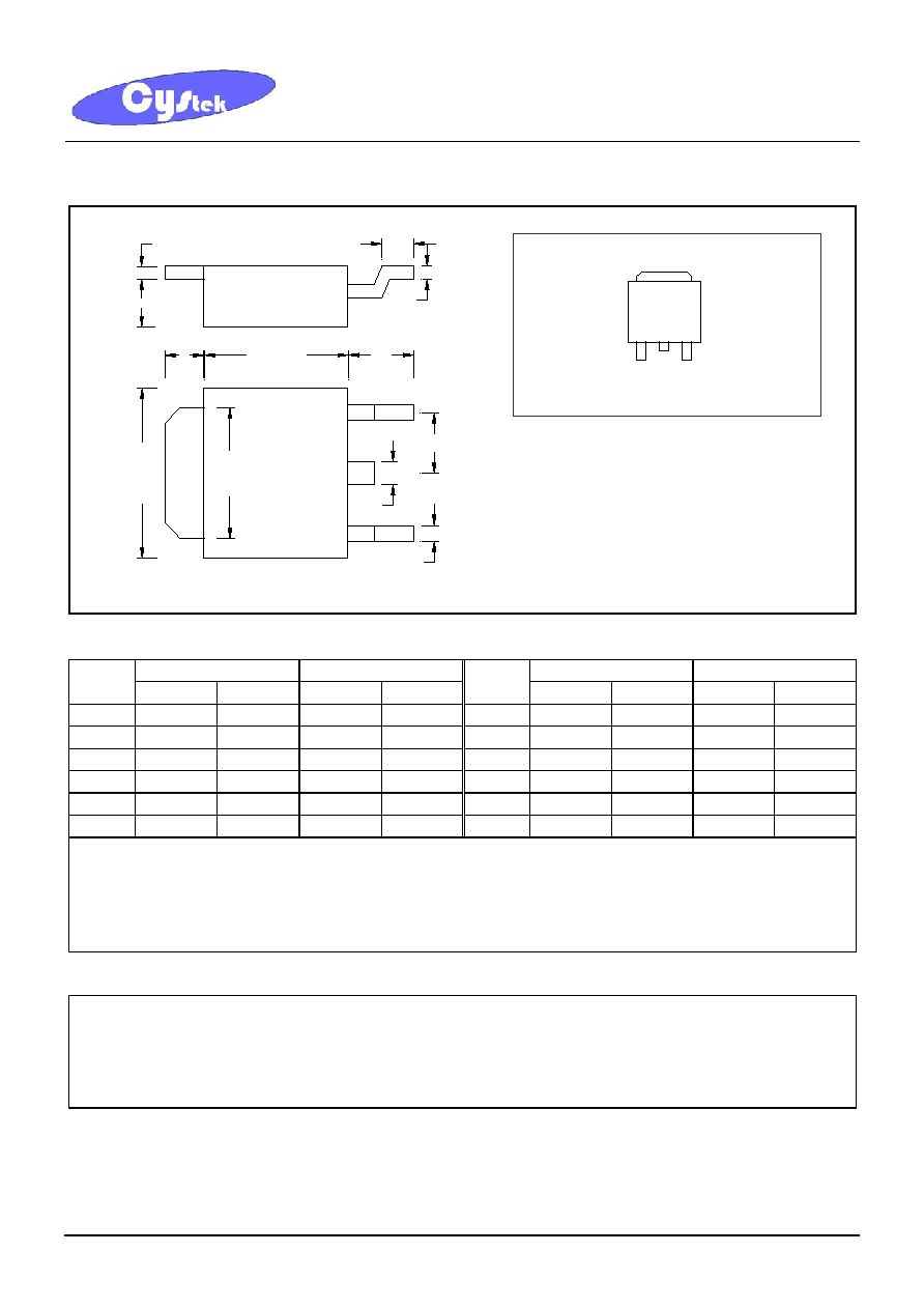
TO-252 Dimension
*: Typical
Inches Millimeters
Inches Millimeters
DIM
Min. Max. Min. Max.
DIM
Min. Max. Min. Max.
A 0.0177
0.0217 0.45 0.55 G 0.0866 0.1102 2.20 2.80
B 0.0650
0.0768
1.65 1.95 H - *0.0906 - *2.30
C
0.0354
0.0591
0.90 1.50 I - 0.0354 - 0.90
D
0.0177
0.0236
0.45 0.60 J - 0.0315 - 0.80
E 0.2520
0.2677 6.40 6.80 K 0.2047 0.2165 5.20 5.50
F 0.2125
0.2283 5.40 5.80 L 0.0551 0.0630 1.40 1.60
Notes:
1.Controlling dimension: millimeters.
2.Maximum lead thickness includes lead finish thickness, and minimum lead thickness is the minimum thickness of base material.
3.If there is any question with packing specification or packing method, please contact your local CYStek sales office.
Material:
·
Lead: 42 Alloy; solder plating
·
Mold Compound: Epoxy resin family, flammability solid burning class: UL94V-0
Important Notice:
·
All rights are reserved. Reproduction in whole or in part is prohibited without the prior written approval of CYStek.
·
CYStek reserves the right to make changes to its products without notice.
·
CYStek semiconductor products are not warranted to be suitable for use in Life-Support Applications, or systems.
·
CYStek assumes no liability for any consequence of customer product design, infringement of patents, or application assistance.
B
A
C
E
H
I
J
K
3
2
1
D
F
G
L
Style: Pin 1.Vin 2.Ground 3.Vout
3-Lead TO-252 Plastic Surface Mount Package
CYStek Package Code: J3
Marking:
78M05