CYStech Electronics Corp.
Spec. No. : C530A3
Issued Date : 2003.04.04
Revised Date : . .
Page No. : 1/3
PL79L05A3
CYStek Product Specification
Three Terminal Low Current Negative Voltage Regulators
PL79L05XA3
Description
The PL79L05XA3 is an inexpensive, easy-to-use device suitable for numerous
applications requiring up to 100mA. Like the higher powered PL7900E3 series
negative regulators, this device features thermal shutdown and current limiting,
making it remarkably rugged. In most applications, no external components are
required for operation.
The PL79L05A3 device is useful for on-card regulation or any other application where a regulated negative voltage
at a modest current level is needed. This regulator offers substantial advantage over the common resistor/zener diode
approach.
∑
No external components required
∑
Internal short circuit current limiting
∑
Internal thermal overload protection
∑
Low cost
∑
Complementary positive regulators offered (PL78L05A3)
∑
Available in either ±3% or ±5% selection.
Absolute Maximum Ratings
(Ta=25
∞
C)
∑
Input Voltage.............................................................................................................-30V
∑
Total Power Dissipation............................................................................... Internally limited
∑
Operating Temperature Range...................................................................... 0
∞
C to +125
∞
C
∑
Maximum Junction Temperature................................................................................+150
∞
C
∑
Storage Temperature Range........................................................................-55
∞
C to +150
∞
C
∑
Lead Temperature (Soldering 10S)......................................
....................................260
∞
C
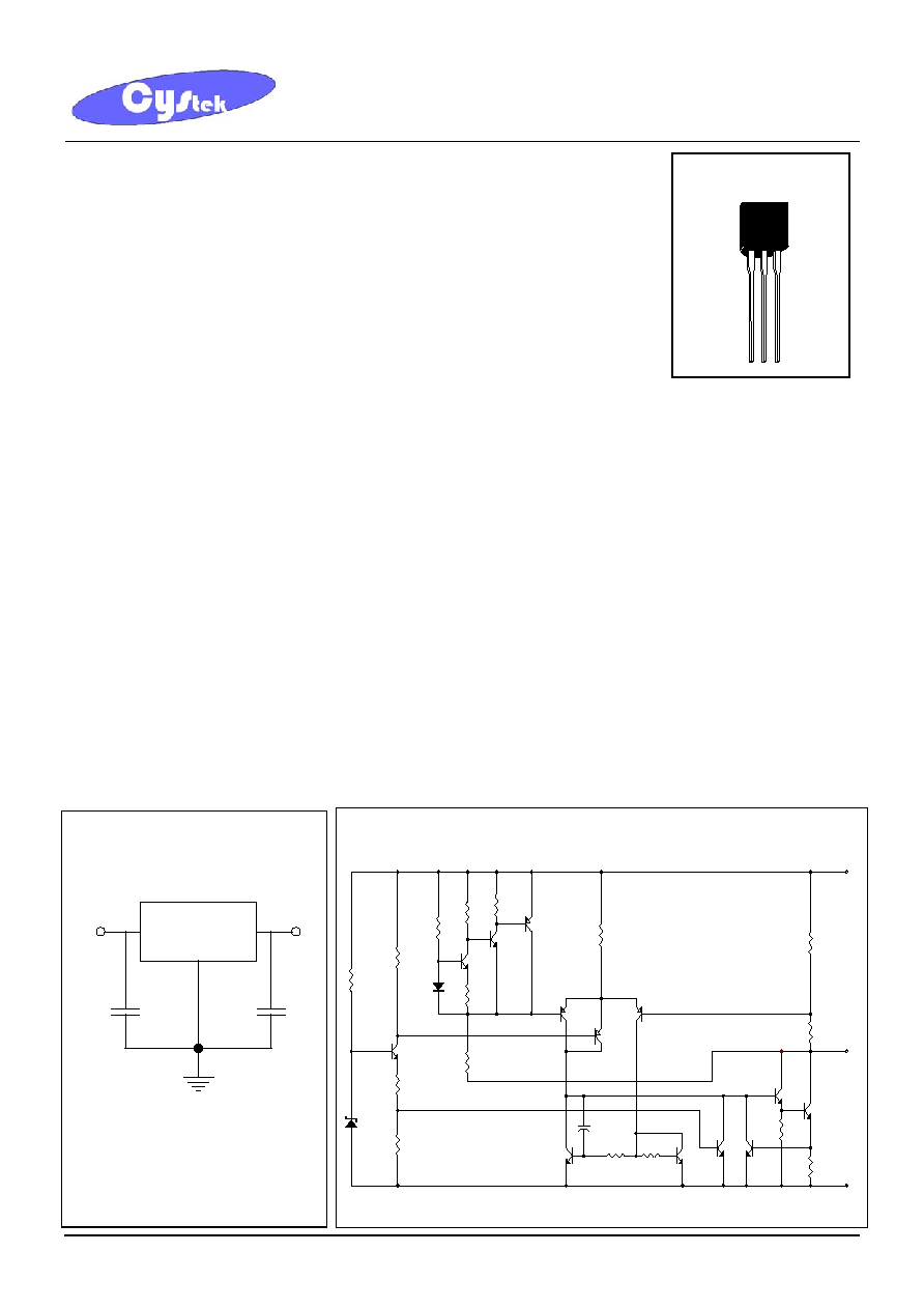
Gnd
R17
R16
Outpu
Q12
R15
Q13
R14
Q11
Q2
Q7
Q6
C
R10
R11
Q9
Q14
Q8
R9
R4
R7
Q4
Q5
R8
R6
Q10
R1
R18
R5
R2
Q1
D1
Z1
Input
R3
Representative Schematic Diagram
Typical Application
TO-92
PL79L05
Vout
Vin
C1
C2
Note:
C1 and C2 are required if regulator is
located far from power supply filter
and load, or oscillation may induced
on the loop.
CYStech Electronics Corp.
Spec. No. : C530A3
Issued Date : 2003.04.04
Revised Date : . .
Page No. : 2/3
PL79L05A3
CYStek Product Specification
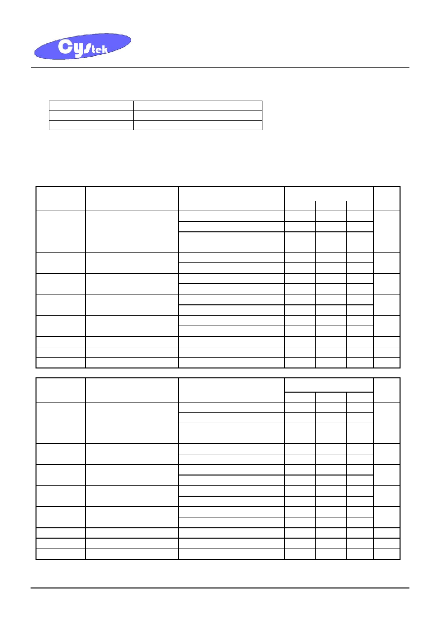
Ordering Information
Device
Output Voltage Tolerance
PL79L05AA3 3%
PL79L05BA3 5%
Electrical Characteristics
Vin=-10V, Iout=40mA, 0
∞
C
Tj
125
∞
C, Cin=0.33uF, Cout=0.1uF (unless otherwise noted)
PL79L05A
Symbol Parameter
Conditions
Min Typ Max
Units
Tj=25
∞
C
-4.85 -5.00 -5.15
1mA
Io
70mA
-4.8 - -5.2
Vo Output
Voltage
1mA
Io
40mA and
-7V
Vin
-20V
-4.8 - -5.2
V
Tj=25
∞
C, -7V
Vin
-20V
- -
150
Vo
Line Regulation
Tj=25
∞
C, -8V
Vin
-20V
- -
100
mV
Tj=25
∞
C, 1mA
Io
100mA
- -
60
Vo
Load Regulation
Tj=25
∞
C, 1mA
Io
40mA
- -
30
mV
Tj=25
∞
C
- - 6
IQ Quiescent
Current
Tj=125
∞
C
- -
5.5
mA
1mA
Io
40mA
- -
0.1
IQ
Quiescent Current
Change
-8V
Vin
-20V
- -
1.5
mA
Vn
Output Noise Voltage
Ta=25
∞
C, 10Hz
f
100KHz
- 40 -
µV
Vin /
Vout Ripple Rejection
-8V
Vin
-18V, f=120Hz
41 49 - dB
VD Dropout
Voltage
Tj=25
∞
C,Iout=40mA
- 1.7 - V
PL79L05B
Symbol Parameter
Conditions
Min Typ Max
Units
Tj=25
∞
C
-4.8 -5.00 -5.2
1mA
Io
70mA
-4.75 - -5.25
Vo Output
Voltage
1mA
Io
40mA and
-7V
Vin
-20V
-4.75 - -5.25
V
Tj=25
∞
C, -7V
Vin
-20V
- -
150
Vo
Line Regulation
Tj=25
∞
C, -8V
Vin
-20V
- -
100
mV
Tj=25
∞
C, 1mA
Io
100mA
- -
60
Vo
Load Regulation
Tj=25
∞
C, 1mA
Io
40mA
- -
30
mV
Tj=25
∞
C
- - 6
IQ Quiescent
Current
Tj=125
∞
C
- -
5.5
mA
1mA
Io
40mA
- -
0.1
IQ
Quiescent Current
Change
-8V
Vin
-20V
- -
1.5
mA
Vn
Output Noise Voltage
Ta=25
∞
C, 10Hz
f
100KHz
- 40 -
µV
Vin /
Vout Ripple Rejection
-8V
Vin
-18V, f=120Hz
41 49 - dB
VD Dropout
Voltage
Tj=25
∞
C,Iout=40mA
- 1.7 - V

CYStech Electronics Corp.
Spec. No. : C530A3
Issued Date : 2003.04.04
Revised Date : . .
Page No. : 3/3
PL79L05A3
CYStek Product Specification
TO-92 Dimension
*: Typical
Inches Millimeters
Inches Millimeters
DIM
Min. Max. Min. Max.
DIM
Min. Max. Min. Max.
A 0.1704
0.1902 4.33 4.83 G 0.0142 0.0220 0.36 0.56
B 0.1704
0.1902 4.33 4.83 H
-
*
0.1000 -
*
2.54
C 0.5000 - 12.70 -
I
-
*
0.0500 -
*
1.27
D 0.0142
0.0220 0.36 0.56
1
-
*
5
∞
-
*
5
∞
E -
*
0.0500 -
*
1.27
2
-
*
2
∞
-
*
2
∞
F 0.1323
0.1480 3.36 3.76
3
-
*
2
∞
-
*
2
∞
Notes:
1.Controlling dimension: millimeters.
2.Maximum lead thickness includes lead finish thickness, and minimum lead thickness is the minimum thickness of base material.
3.If there is any question with packing specification or packing method, please contact your local CYStek sales office.
Material:
∑
Lead: 42 Alloy ; solder plating
∑
Mold Compound: Epoxy resin family, flammability solid burning class: UL94V-0
Important Notice:
∑
All rights are reserved. Reproduction in whole or in part is prohibited without the prior written approval of CYStek.
∑
CYStek reserves the right to make changes to its products without notice.
∑
CYStek semiconductor products are not warranted to be suitable for use in Life-Support Applications, or systems.
∑
CYStek assumes no liability for any consequence of customer product design, infringement of patents, or application assistance.
79L05
3
1
A
D
B
C
I
1
E
F
2
3
G
H
2
Style: Pin 1.GND 2.Vin 3.Vout
3-Lead TO-92 Plastic Package
CYStek Package Code: A3