 | –≠–ª–µ–∫—Ç—Ä–æ–Ω–Ω—ã–π –∫–æ–º–ø–æ–Ω–µ–Ω—Ç: ZD33V0 | –°–∫–∞—á–∞—Ç—å:  PDF PDF  ZIP ZIP |
CYStech Electronics Corp.
Spec. No. : C346S2
Issued Date : 2004.04.12
Revised Date :
Page No. : 1/4
ZD02V4S2 series
CYStek Product Specification
200mW SOD-323 Zener Voltage Regulators
ZD02V4S2 Series
Description
The ZD02V4S2 series zener diodes are packaged in a SOD-323 surface mount package that has a power dissipation
of 200mW. They are designed to provide voltage regulation protection and are especially attractive in situations
where space is at a premium. They are well suited for applications such as cellular phones, hand held portables, and
high density PC boards.
Features
∑
Standard zener breakdown voltage range : 2.4V to 75V
∑
Steady state power rating of 200mW..
∑
Small body outline dimensions : 0.067 inches◊0.049 inches (1.7mm◊1.25mm)
∑
Low body height : 0.035 inches (0.9mm)
∑
Package weight : 4.507 mg/unit
∑
ESD rating of class 3 (>16kV) per human body model.
Mechanical Data
∑
Case : Void free , transfer molded plastic.
∑
Finish : All external surfaces are corrosion resistant
∑
Maximum case temperature for soldering purposes : 260 for 10 seconds
∑
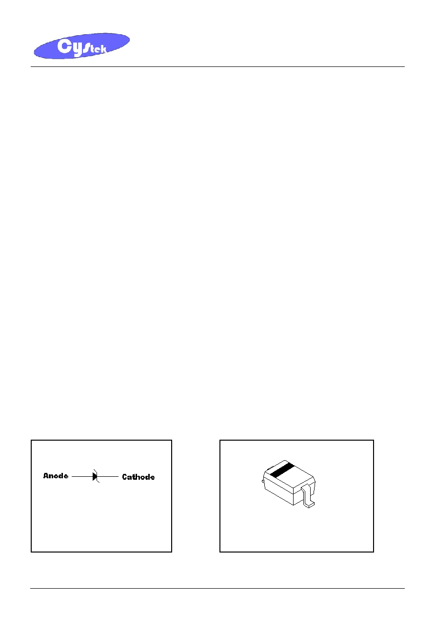
Polarity : Cathode indicated by polarity band.
∑
Leads : Plated with Sn/Pb for ease of solderability.
∑
Flammability rating : UL94 V-0
∑
Mounting position : Any
Symbol Outline
SOD-323
CYStech Electronics Corp.
Spec. No. : C346S2
Issued Date : 2004.04.12
Revised Date :
Page No. : 2/4
ZD02V4S2 series
CYStek Product Specification
Absolute Maximum Ratings
(Ta=25, unless otherwise specified)
∑
Maximum Temperatures
Storage Temperature Tstg ................................................................................................... -65~+150
∞
C
Junction Temperature Tj............................................................................. -65~ +150
∞
C
∑
Maximum Power Dissipation
Total Power Dissipation Ptot
(Note)
........................................................................................... 200 mW
Derate above 25 .................................................................................... 1.5mW/
∑
Thermal Resistance, Junction to Ambient Air R
JA
.....................................................635/W
Note : Parts mounted on FR-5 board with minimum pad.
Electrical Characteristics
(TA=25 unless otherwise noted, V
F
=0.9V Max @I
F
=10mA for all types.)
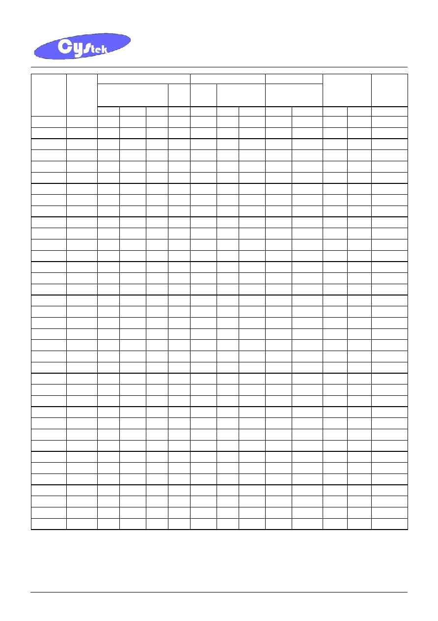
Symbol Parameter
V
Z
Reverse zener voltage @ I
ZT
I
ZT
Reverse
current
Z
ZT
Maximum zener impedance @ I
ZT
I
ZK
Reverse
current
Z
ZK
Maximum zener impedance @ I
ZK
I
R
Reverse leakage current @ V
R
V
R
Reverse
voltage
I
F
Forward
current
V
F
Forward voltage @ I
F
V
Z
Maximum temperature coefficient of V
Z
C
Maximum capacitance @ V
R
=0V and f=1MHz
CYStech Electronics Corp.
Spec. No. : C346S2
Issued Date : 2004.04.12
Revised Date :
Page No. : 3/4
ZD02V4S2 series
CYStek Product Specification
Zener voltage(Note 2)
Zener impedance
Leakage Current
V
Z
(volts) @I
ZT
Z
ZT
@
I
ZT
Z
ZK
@I
ZK
I
R
@V
R
V
Z
(mV/K)
@I
ZT
C
@V
R
=0V
f=1MHz
Device
Marking
Code
min nom max mA
mA µA V min max pF
ZD02V4 00 2.2 2.4 2.6 5 100 1000 0.5 50 1.0 -3.5 0 450
ZD02V7 01 2.5 2.7 2.9 5 100 1000 0.5 20 1.0
-3.5
0 450
ZD03V0 02 2.8 3.0 3.2 5 100 1000 0.5 10 1.0
-3.5
0 450
ZD03V3 05 3.1 3.3 3.5 5 95 1000 0.5 5 1.0
-3.5
0 450
ZD03V6 06 3.4 3.6 3.8 5 90 1000 0.5 5 1.0
-3.5
0 450
ZD03V9 07 3.7 3.9 4.1 5 90 1000 0.5 3 1.0 -3.5 -2.5 450
ZD04V3 08 4.0 4.3 4.6 5 90 1000 0.5 3 1.0 -3.5 0 450
ZD04V7 09 4.4 4.7 5.0 5 80 800 0.5 3 2.0 -3.5 0.2 260
ZD05V1 0A 4.8 5.1 5.4 5 60 500 0.5 2 2.0 -2.7 1.2 225
ZD05V6 0C 5.2 5.6 6.0 5 40 200 0.5 1 2.0 -2.0 2.5 200
ZD06V2 0E 5.8 6.2 6.6 5 10 100 0.5 3 4.0 0.4 3.7 185
ZD06V8 0F 6.4 6.8 7.2 5 15 160 0.5 2 4.0 1.2 4.5 155
ZD07V5 0G 7.0 7.5 7.9 5 15 160 0.5 1 5.0 2.5 5.3 140
ZD08V2 0H 7.7 8.2 8.7 5 15 160 0.5 0.7 5.0 3.2 6.2 135
ZD09V1 0K 8.5 9.1 9.6 5 15 160 0.5 0.2 7.0 3.8 7.0 130
ZD10V0 0L 9.4 10 10.6 5 20 160 0.5 0.1 8.0 4.5 8.0 130
ZD11V0 0M 10.4 11 11.6 5 20 160 0.5 0.1 8.0 5.4 9.0 130
ZD12V0 0N 11.4 12 12.7 5 25 80 0.5 0.1 8.0 6.0 10 130
ZD13V2 0P 12.4 13.25 14.1 5
30 80 0.5 0.1
8.0
7.0 11
120
ZD15V0 0T 14.3 15 15.8 5 30 80 0.5 0.05 10.5 9.2 13 110
ZD16V2 0U 15.3 16.2 17.1 5 40 80 0.5 0.05 11.2 10.4 14
105
ZD18V0 0W 16.8 18 19.1 5 45 80 0.5 0.05 12.6 12.4 16 100
ZD20V0 0Z 18.8 20 21.2 5 55 100 0.5 0.05 14.0 14.4 18 85
ZD22V0 10 20.8 22 23.3 5 55 100 0.5 0.05 15.4 16.4 20 85
ZD24V2 11 22.8 24.2 25.6 5 70 120 0.5 0.05 16.8 18.4 22
80
ZD27V0 12 25.1 27 28.9 2 80 300 0.5 0.05 18.9 21.4 25.3 70
ZD30V0 14 28 30 32 2 80 300 0.5 0.05 21.0 24.4
29.4 70
ZD33V0 18 31 33 35 2 80 300 0.5 0.05 23.2 27.4
33.4 70
ZD36V0 19 34 36 38 2 90 500 0.5 0.05 25.2 30.4
37.4 70
ZD39V0 20 37 39 41 2 130 500 0.5 0.05 27.3 33.4
41.2 45
ZD43V0 21 40 43 46 2 150 500 0.5 0.05 30.1 37.6
46.6 40
ZD47V0 1A 44 47 50 2 170 500 0.5 0.05 32.9 42.0
51.8 40
ZD51V0 1C 48 51 54 2 180 500 0.5 0.05 35.7 46.6
57.2 40
ZD56V0 1D 52 56 60 2 200 500 0.5 0.05 39.2 52.2
63.8 40
ZD62V0 1E 58 62 66 2 215 500 0.5 0.05 43.4 58.8
71.6 35
ZD68V0 1F 64 68 72 2 240 500 0.5 0.05 47.6 65.6
79.8 35
ZD75V0 1G 70 75 79 2 255 500 0.5 0.05 52.5 73.4
88.6 35
Note 2: Zener voltage is measured with a pulse test current I
Z
at an ambient temperature of 25.
CYStech Electronics Corp.
Spec. No. : C346S2
Issued Date : 2004.04.12
Revised Date :
Page No. : 4/4
ZD02V4S2 series
CYStek Product Specification
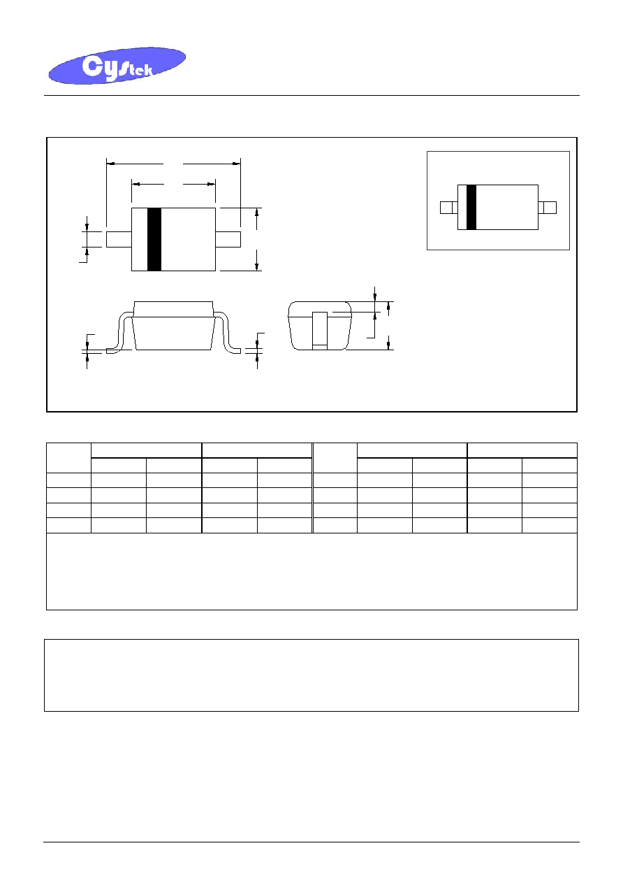
SOD-323 Dimension
*: Typical
Inches Millimeters
Inches Millimeters
DIM
Min. Max. Min. Max.
DIM
Min. Max. Min. Max.
A
0.0630
0.0709
1.60
1.80
E
0.0060 - 0.15 -
B 0.0453
0.0531 1.15 1.35 H 0.0000 0.0040 0.00 0.10
C 0.0315
0.0394 0.80 1.00 J 0.0035
0.0070
0.089 0.177
D 0.0098
0.0157 0.25 0.40 K 0.0906 0.1063 2.30 2.70
Notes:
1.Controlling dimension : millimeters.
2.Lead thickness specified per L/F drawing with solder plating.
3.If there is any question with packing specification or packing method, please contact your local CYStek sales office.
Material:
∑
Lead: 42 Alloy ; solder plating
∑
Mold Compound: Epoxy resin family, flammability solid burning class: UL94V-0
Important Notice:
∑
All rights are reserved. Reproduction in whole or in part is prohibited without the prior written approval of CYStek.
∑
CYStek reserves the right to make changes to its products without notice.
∑
CYStek semiconductor products are not warranted to be suitable for use in Life-Support Applications, or systems.
∑
CYStek assumes no liability for any consequence of customer product design, infringement of patents, or application assistance.
D
A
H
J
K
C
E
B
1
2
Style: Pin 1.Cathode 2.Anode
2-Lead SOD-323 Plastic
Surface Mounted Package
CYStek Package Code: S2
Marking:
5 H
XX