SBR5030 THRU SBR5060
CURRENT 50.0Amperes
VOLTAGE 30 to 60 Volts
Maximum Ratings and Electrical Characteristics
Notes:
(1) Pulse test: 300S pulse width, 1% duty cycle
(2) Thermal resistance from junction to case
(Ratings at 25 ambient temperature unless otherwise specified, single phase, half wave, resistive or inductive
load. For capacitive load, derate by 20%)
Features
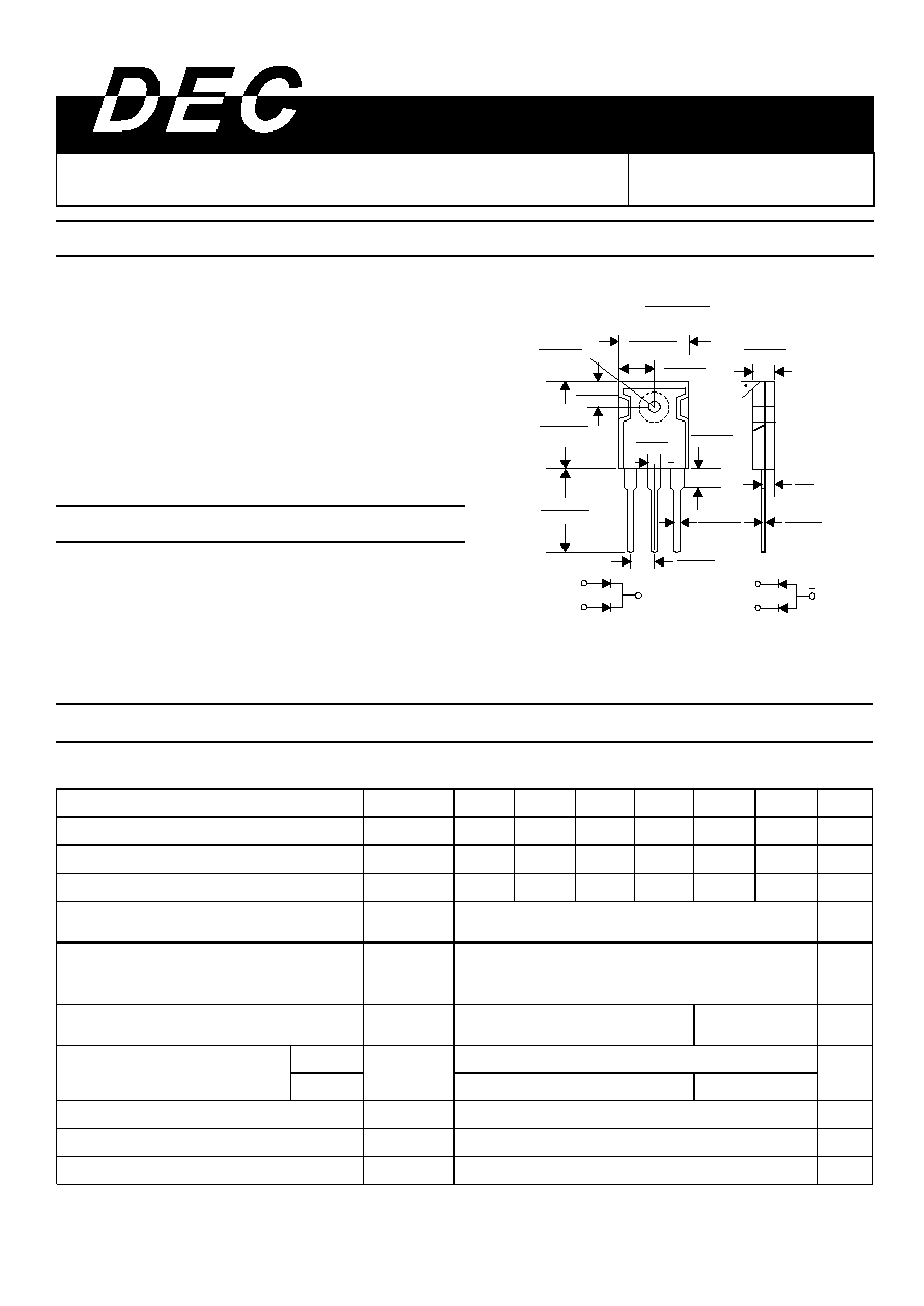
Mechanical Data
∑ Plastic Package has Underwriters Laboratory
Flammability Classification 94V-0
∑ Metal silicon junction, majority carrier conduction
∑ Guard ring for overvoltage protection
∑ Low power loss, high efficiency
∑ High current capability, Low forward voltage drop
∑ High surge capability
∑ For use in low voltage, high frequency inverters,
free wheeling, and polarity protection applications
∑ Dual rectifier construction
∑ High temperature soldering guaranteed:
250/10 seconds, 0.17" (4.3mm) from case
∑ Case : JEDEC TO-3P molded plastic body
∑ Terminals : Lead solderable per
MIL-STD-750, Method 2026
∑ Polarity : As marked. No suffix indicates Common
Cathode, suffix "A" indicates Common Anode
∑ Mounting Position : Any
∑ Weight : 0.20ounce, 5.6 grams
Symbols
SBR5035
Units
Maximum repetitive peak reverse voltage
V
RRM
30
35
Volts
Maximum RMS voltage
V
RMS
0.65
0.70
Maximum DC blocking voltage
V
DC
Volts
Maximum average forward rectified current
at V
R
(equiv.)<0.2
VR(DC)
(See Fig 1)
I(
AV
)
50.0
Amps
Peak forward surge current 8.3ms single half
sine-wave superimposed on rated load
(JEDEC method)
400.0
Amps
Maximum instantaneous forward voltage
at 25A (Note 1)
V
F
10.0
Volts
T
A
=25
100
Maximum instantaneous reverse
current at rated DC blocking
voltage (Note1)
T
A
=125
mA
Typical thermal resistance (Note 2)
/W
Operating junction temperature range
I
R
I
FSM
T
J
Volts
SBR5030
21
24
30
35
Storage temperature range
T
STG
-65 to +150
SBR5040
40
60
SBR5060
28
42
40
60
R
JC
1.4
150
50
SBR5050
35
50
-65 to +125
SBR5045
45
32
45
Dimensions in inches and (millimeters)
TO-3P
.635(16.13)
.840(21.34)
.800(20.32)
.320(8.13)
.12(3.0)
.170(4.32)
.050(1.27)
.205(5.21)
.225(5.7)
.030(0.8)
.120(3.05)
.180(4.53)
.625(15.88)
.820(20.83)
.770(19.56)
.310(7.87)
.11(2.8)
.150(3.81)
.045(1.14)
.195(4.49)
.205(5.2)
.020(0.5)
.115(2.92)
.170(4.32)
DIA.
.095
(2.4)
30
+
PIN 1
PIN 3
PIN 2
CASE
Positive CT
Suffix "C"
PIN 1
PIN 3
PIN 2
CASE
Negative CT
Suffix "A"
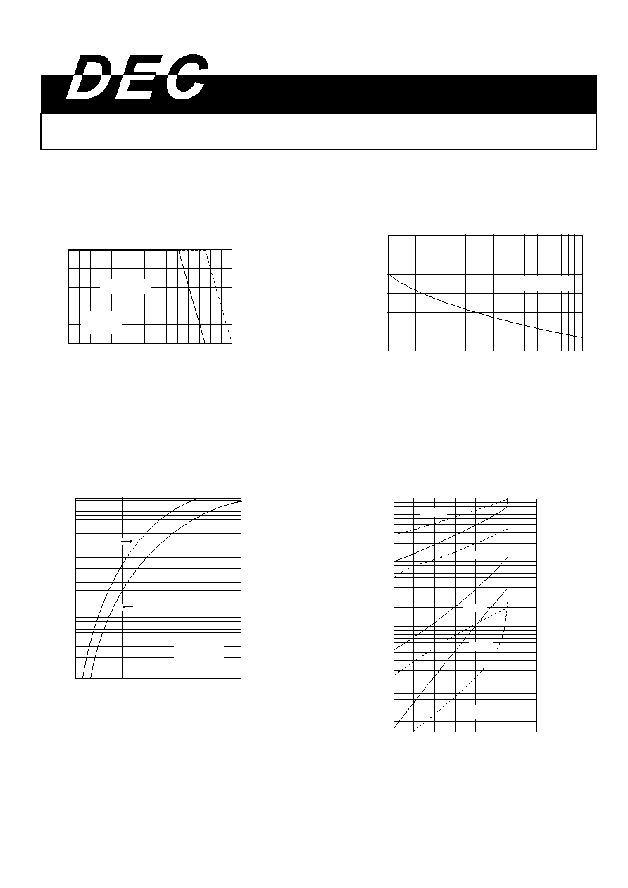
SINGLE PHASE
HALF WAVE 50Hz
INDUCTIVE OR
RESISTIVE LOAD
SBR5030-SBR5045
- - - SBR5050-SBR5060
FIG.1-FORWARD CURRENT DERATING CURVE
A
V
E
R
A
G
E
F
O
R
W
A
R
D
C
U
R
R
E
N
T
A
M
P
E
R
E
S
LEAD TEMPERATURE ()
0
150
100
50
0
30
40
20
10
50
SBR5030-SBR5045
SBR5050-SBR5060
T
J
=25
PULSE WIDTH=300
1% DUTY CYCLE
I
N
S
T
A
N
T
A
N
E
O
U
S
F
O
R
W
A
R
D
C
U
R
R
E
N
T
(
A
M
P
E
R
E
S
)
INSTANTANEOUS FORWARD VOLTAGE (VOLTS)
0.1
100
10
1.0
FIG.2-TYPICAL INSTANTANEOUS
FORWARD CHARACTERISTICS
0.4
1.0
0.8
0.6
0.5
0.9
0.7
0.3
FIG.5-MAXIMUM NON-REPETITIVE PEAK
FORWARD SURGE CURRENT
P
E
A
K
F
O
R
W
A
R
D
S
U
R
G
E
C
U
R
R
E
N
T
(
A
M
P
E
R
E
S
)
NUMBER OF CYCLES AT 60Hz
8.3ms SINGLE HALF SINE-WAVE
(JEDEC Method)
0
200
600
300
100
400
500
1.0
100
10
50
20
5.0
2.0
T
C
=25
T
C
=150
T
C
=125
T
C
=75
FIG.3-TYPICAL REVERSE CHARACTERISTICS
PERCENT OF RATED PEAK REVERSE VOLTAGE
I
N
S
T
A
N
T
A
N
E
O
U
S
R
E
V
E
R
S
E
C
U
R
R
E
N
T
M
I
L
L
(
A
M
P
E
R
E
S
)
0.001
10
1.0
0.1
0.01
100
80
60
40
20
140
120
SBR5030-SBR5045
- - - SBR5050-SBR5060
RATINGS AND CHARACTERISTIC CURVES SBR5030-SBR5060