
General Description
The DS1110 delay line is an improved replacement for
the DS1010. It has ten equally spaced taps providing
delays from 5ns to 500ns. The devices are offered in a
standard 16-pin SO or 14-pin TSSOP. The DS1110 series
delay lines provide a nominal accuracy of ±5% or ±2ns,
whichever is greater, at 5V and +25∞C. The DS1110
reproduces the input logic state at the tap 10 output after
a fixed delay as specified by the dash number extension
of the part number. The DS1110 is designed to produce
both leading- and trailing-edge delays with equal preci-
sion. Each tap is capable of driving up to ten 74LS type
loads. Dallas Semiconductor can customize standard
products to meet special needs.
Features
All-Silicon, 5V, 10-Tap Delay Line
Improved, Drop-In Replacement for the DS1010
10 Taps Equally Spaced
Delays are Stable and Precise
Leading- and Trailing-Edge Accuracy
Delay Tolerance ±5% or ±2ns, whichever is
Greater, at 5V and +25∞C
Economical
Auto-Insertable, Low Profile
Low-Power CMOS
TTL/CMOS Compatible
Vapor Phase, IR, and Wave Solderable
Fast-Turn Prototypes
Delays Specified Over Commercial and Industrial
Temperature Ranges
Custom Delays Available
Standard 16-Pin SO or 14-Pin TSSOP
DS1110
10-Tap Silicon Delay Line
_____________________________________________ Maxim Integrated Products
1
TOP VIEW
14
13
12
11
10
9
8
1
2
3
4
5
6
7
V
CC
TAP1
TAP3
TAP5
TAP4
TAP2
N.C.
IN
TAP7
TAP9
TAP10
GND
TAP8
TAP6
TSSOP
DS1110E
Pin Configurations
Ordering Information
Rev 1; 11/03
For pricing, delivery, and ordering information, please contact Maxim/Dallas Direct! at
1-888-629-4642, or visit Maxim's website at www.maxim-ic.com.
PART
TEMP RANGE
PIN-PACKAGE
DS1110E-XXX
-40
∞C to +85∞C
14 TSSOP
DS1110S-XXX
-40
∞C to +85∞C
16 SO
Applications
Communications Equipment
Medical Devices
Automated Test Equipment
PC Peripheral Devices
Selector Guide appears at end of data sheet.
Pin Configurations continued at end of data sheet.

DS1110
10-Tap Silicon Delay Line
2
______________________________________________________________________
ABSOLUTE MAXIMUM RATINGS
DC ELECTRICAL CHARACTERISTICS
(V
CC
= 5.0V ±5%, T
A
= -40∞C to +85∞C.)
Stresses beyond those listed under "Absolute Maximum Ratings" may cause permanent damage to the device. These are stress ratings only, and functional
operation of the device at these or any other conditions beyond those indicated in the operational sections of the specifications is not implied. Exposure to
absolute maximum rating conditions for extended periods may affect device reliability.
Voltage on Any Pin Relative to Ground .................-0.5V to +6.0V
Operating Temperature Range ...........................-40
∞C to +85∞C
Storage Temperature Range .............................-55
∞C to +125∞C
Soldering Temperature...................See IPC/JEDEC J-STD-020A
PARAMETER
SYMBOL
CONDITIONS
MIN
TYP
MAX
UNITS
Supply Voltage
V
CC
(Note 1)
4.75
5.0
5.25
V
High-Level Input Voltage
V
IH
(Note 1)
2.4
V
CC
+ 0.3
V
Low-Level Input Voltage
V
IL
(Note 1)
-0.3
+0.8
V
Input Leakage Current
I
I
0V
V
I
V
CC
-1.0
+1.0
µA
Active Current
I
CC
V
CC
= max, period = min (Note 2)
40
150
mA
High-Level Output Current
I
OH
V
CC
= min, V
OH
= 2.3V
-1.0
mA
Low-Level Output Current
I
OL
V
CC
= min, V
OL
= 0.5V
12
mA
AC ELECTRICAL CHARACTERISTICS
(V
CC
= 5.0V ±5%, T
A
= -40∞C to +85∞C.)
PARAMETER
SYMBOL
CONDITIONS
MIN
TYP
MAX
UNITS
Input Pulse Width
t
WI
(Note 6)
10% of
tap 10
ns
+25∞C, 5.0V (Notes 3, 5, 6, 7, 9)
-2
Table 1
+2
0∞C to +70∞C (Notes 4≠7)
-3
Table 1
+3
Input-to-Tap Delay
(Delays
40ns)
t
PLH
t
PHL
-40∞C to +85∞C (Notes 4≠7)
-4
Table 1
+4
ns
+25∞C, 5.0V (Notes 3, 5, 6, 7, 9)
-5
Table 1
+5
0∞C to +70∞C (Notes 4≠7)
-8
Table 1
+8
Input-to-Tap Delay
(Delays > 40ns)
t
PLH
t
PHL
-40∞C to +85∞C (Notes 4≠7)
-13
Table 1
+13
%
Power-Up Time
t
PU
200
ms
Input Period
Period
(Note 8)
2 (t
WI
) or 20,
whichever
is greater
ns
DS1110
10-Tap Silicon Delay Line
_____________________________________________________________________
3
Note 1: All voltages are referenced to ground.
Note 2: Measured with outputs open.
Note 3: Initial tolerances are ± with respect to the nominal value at +25∞C and V
CC
= 5.0V for both leading and trailing edges.
Note 4: Temperature and voltage tolerances are with respect to the actual delay measured over stated temperature range and a 4.75V
to 5.25V range.
Note 5: Intermediate delay values are available on a custom basis.
Note 6: See Test Conditions section.
Note 7: All tap delays tend to vary unidirectionally with temperature or voltage changes. For example, if tap 1 slows down, all other
taps also slow down; tap 3 can never be faster than tap 2.
Note 8: Pulse width and period specifications may be exceeded; however, accuracy is application sensitive (decoupling, layout, etc.)
Note 9: For Tap 1 delays greater than 20ns, the tolerance is ±3ns or ±5%, whichever is greater.
CAPACITANCE
(T
A
= +25∞C.)
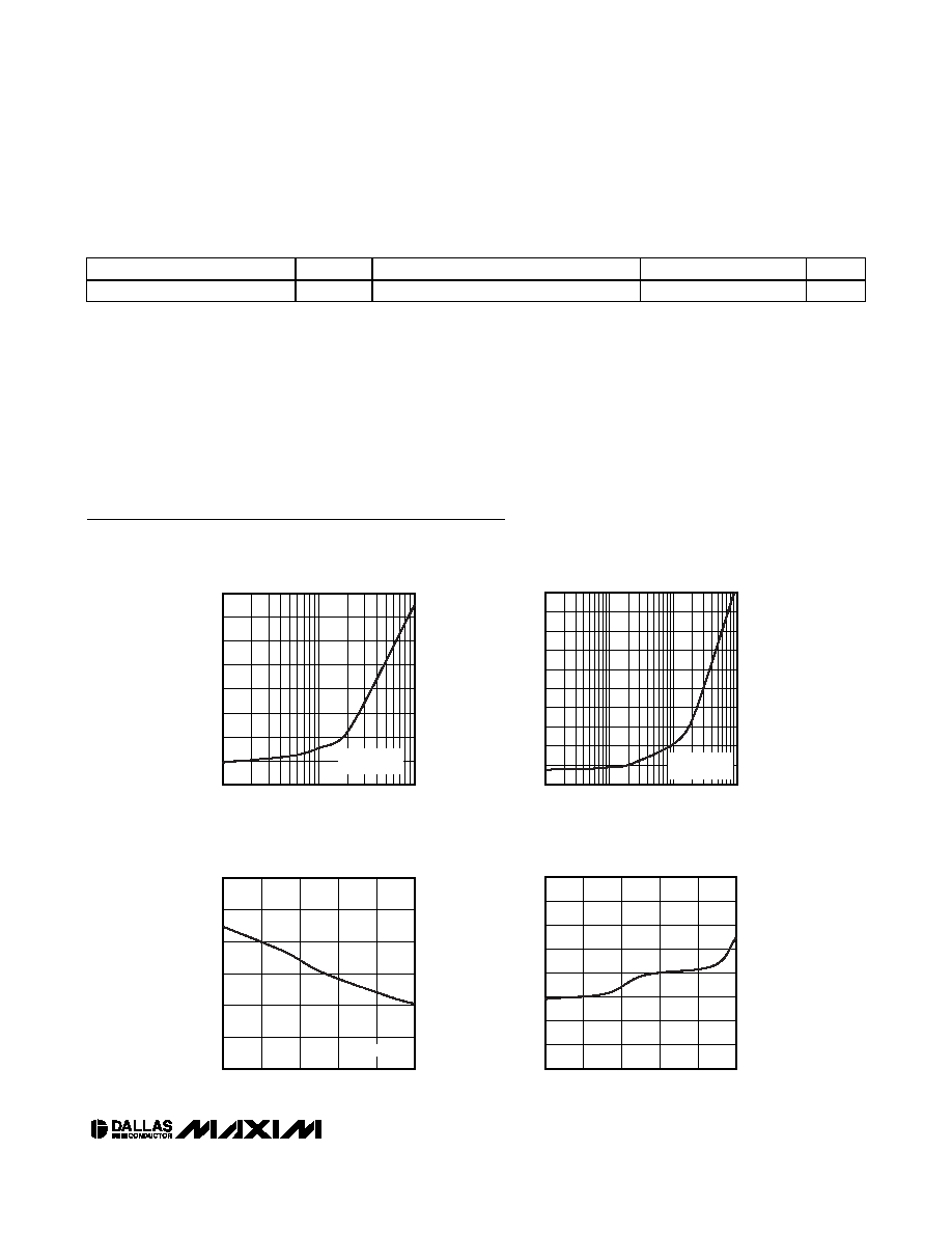
Typical Operating Characteristics
(V
CC
= 5.0V, T
A
= +25∞C, unless otherwise noted.)
PARAMETER
SYMBOL
CONDITIONS
MIN
TYP
MAX
UNITS
Input Capacitance
C
IN
5
10
pF
47
48
49
50
51
52
53
54
46
DS1110-50 TAP 10 DELAY
vs. TEMPERATURE
DS1110 toc04
TEMPERATURE (
∞C)
DELAY (ns)
60
35
10
-15
-40
85
DS1110-500 TAP 10 DELAY
vs. TEMPERATURE
DS1110 toc03
TEMPERATURE (
∞C)
DELAY (ns)
60
35
10
-15
450
475
500
525
550
575
425
-40
85
500kHz INPUT
10
1.0
20
40
60
80
100
120
140
160
180
200
0
0.1
100
DS1110-50 ACTIVE CURRENT
vs. INPUT FREQUENCY
DS1110 toc02
FREQUENCY (MHz)
ACTIVE CURRENT (mA)
15pF LOAD/TAP
V
CC
= 5.25V
DS1110-500 ACTIVE CURRENT
vs. INPUT FREQUENCY
DS1110 toc01
FREQUENCY (MHz)
ACTIVE CURRENT (mA)
1.0
5
10
15
20
25
30
35
40
0
0.1
10
15pF LOAD/TAP
V
CC
= 5.25V
DS1110
10-Tap Silicon Delay Line
4
______________________________________________________________________
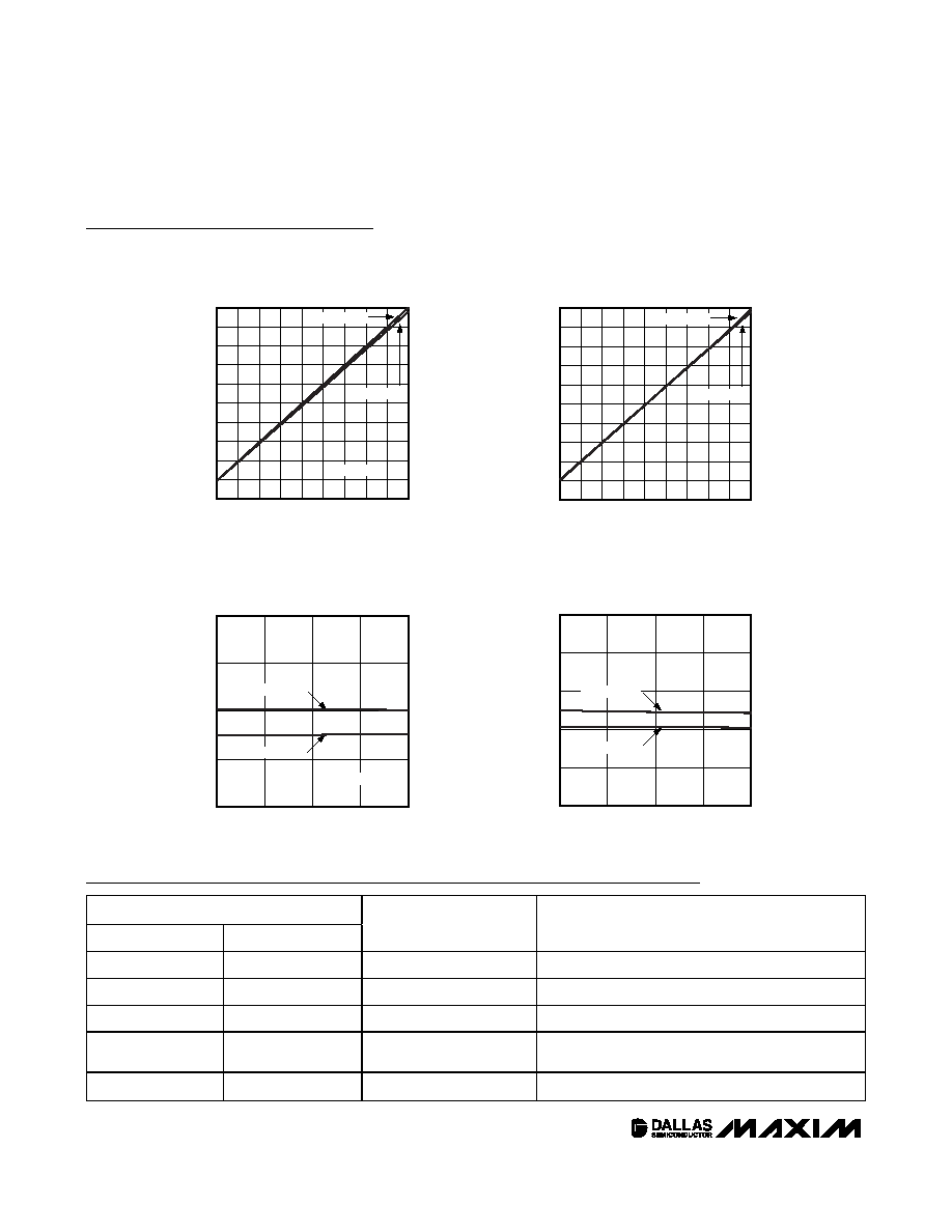
Typical Operating Characteristics (continued)
(V
CC
= 5.0V, T
A
= +25∞C, unless otherwise noted.)
47
49
51
53
55
45
DS1110-50 TAP 10 DELAY
vs. VOLTAGE
DS1110 toc08
VOLTAGE (V)
DELAY (ns)
5.125
5.000
4.875
4.750
5.250
FALLING EDGE
RISING EDGE
DS1110-500 TAP 10 DELAY
vs. VOLTAGE
DS1110 toc07
VOLTAGE (V)
DELAY (ns)
5.125
5.000
4.875
480
500
520
540
460
4.750
5.250
FALLING EDGE
RISING EDGE
500kHz INPUT
DS1110-50 DELAY vs. TAP
DS1110 toc06
TAP
DELAY (ns)
9
8
6
7
3
4
5
2
5
10
15
20
25
30
35
40
45
50
0
1
10
FALLING EDGE
RISING EDGE
DS1110-500 DELAY vs. TAP
DS1110 toc05
TAP
DELAY (ns)
9
8
6
7
3
4
5
2
50
100
150
200
250
300
350
400
450
500
0
1
10
FALLING EDGE
RISING EDGE
500kHz INPUT
Pin Description
PIN
TSSOP
SO
NAME
FUNCTION
1
1
IN
Input
2
2, 3, 15
N.C.
No Connection
7
8
GND
Ground
13, 3, 12, 4, 11,
5, 10, 6, 9, 8
14, 4, 13, 5, 12, 6, 11,
7, 10, 9
Tap 1≠Tap 10
Tap Output Number
14
16
V
CC
5.0V

Detailed Description
The DS1110 delay line is an improved replacement for
the DS1010. It has ten equally spaced taps providing
delays from 5ns to 500ns. The devices are offered in a
standard 16-pin SO or 14-pin TSSOP. The DS1110
series delay lines provide a nominal accuracy of ±5%
or ±2ns, whichever is greater, at 5V and +25∞C. The
DS1110 reproduces the input logic state at the tap 10
output after a fixed delay as specified by the dash
number extension of the part number. The DS1110 is
designed to produce both leading- and trailing-edge
delays with equal precision. Each tap is capable of dri-
ving up to ten 74LS type loads. Dallas Semiconductor
can customize standard products to meet special
needs. For special requests call 972-371-4348.
DS1110
10-Tap Silicon Delay Line
_____________________________________________________________________
5
10%
10%
IN
TAP1
TAP2
TAP9
TAP10
10%
10%
Figure 1. Logic Diagram
PART
TOTAL DELAY* (ns)
DELAY/TAP (ns)
DS1110-50
50
5
DS1110-60
60
6
DS1110-75
75
7.5
DS1110-80
80
8
DS1110-100
100
10
DS1110-125
125
12.5
DS1110-150
150
15
DS1110-175
175
17.5
DS1110-200
200
20
DS1110-250
250
25
DS1110-300
300
30
DS1110-350
350
35
DS1110-400
400
40
DS1110-450
450
45
DS1110-500
500
50
Table 1. Part Number by Delay (t
PHL
, t
PLH
)
V
IL
IN
OUT
0.8V
V
IH
t
RISE
2.2V
1.5V
1.5V
1.5V
1.5V
1.5V
0.8V
2.2V
PERIOD
t
WI
t
PLH
t
PLH
t
FALL
t
WI
Figure 2. Timing Diagram: Silicon Delay Line
*Custom delays are available.