
General Description
The DS1110L 10-tap delay line is a 3V version of the
DS1110. It has 10 equally spaced taps providing delays
from 10ns to 500ns. The DS1110L series delay lines
provide a nominal accuracy of ±5% or ±2ns, whichever
is greater, at 3.3V and +25∞C. The DS1110L is character-
ized to operate from 2.7V to 3.6V. The DS1110L
produces both leading- and trailing-edge delays with
equal precision. The device is offered in a standard
14-pin TSSOP.
Features
All-Silicon Delay Line
3V Version of the DS1110
10 Taps Equally Spaced
Delays Are Stable and Precise
Leading- and Trailing-Edge Accuracy
Delay Tolerance ±5% or ±2ns, Whichever Is
Greater, at 3.3V and +25∞C
Economical
Low-Profile 14-Pin TSSOP
Low-Power CMOS
TTL/CMOS Compatible
Vapor Phase and IR Solderable
Fast-Turn Prototypes
Delays Specified Over Commercial and Industrial
Temperature Ranges
Custom Delays Available
DS1110L
3V 10-Tap Silicon Delay Line
_____________________________________________ Maxim Integrated Products
1
14
13
12
11
10
9
8
1
2
3
4
5
6
7
V
CC
TAP1
TAP3
TAP5
TAP4
TAP2
N.C.
IN
TOP VIEW
TAP7
TAP9
TAP10
GND
TAP8
TAP6
TSSOP (173mil)
DS1110L
Pin Configuration
Ordering Information
XX-XXXX; Rev 1; 11/03
For pricing, delivery, and ordering information, please contact Maxim/Dallas Direct! at
1-888-629-4642, or visit Maxim's website at www.maxim-ic.com.
PART
TEM P RANGE
PIN-
PACKAGE
TOTAL
DELAY
( ns) *
DS1110LE-100
-40∞C to +85∞C
14 TSSOP (173mil)
100
DS1110LE-125
-40∞C to +85∞C
14 TSSOP (173mil)
125
DS1110LE-150
-40∞C to +85∞C
14 TSSOP (173mil)
150
DS1110LE-175
-40∞C to +85∞C
14 TSSOP (173mil)
175
DS1110LE-200
-40∞C to +85∞C
14 TSSOP (173mil)
200
DS1110LE-250
-40∞C to +85∞C
14 TSSOP (173mil)
250
DS1110LE-300
-40∞C to +85∞C
14 TSSOP (173mil)
300
DS1110LE-350
-40∞C to +85∞C
14 TSSOP (173mil)
350
DS1110LE-400
-40∞C to +85∞C
14 TSSOP (173mil)
400
DS1110LE-450
-40∞C to +85∞C
14 TSSOP (173mil)
450
DS1110LE-500
-40∞C to +85∞C
14 TSSOP (173mil)
500
*Custom delays are available.
Applications
Communications Equipment
Medical Devices
Automated Test Equipment
PC Peripheral Devices

DS1110L
3V 10-Tap Silicon Delay Line
2
______________________________________________________________________
ABSOLUTE MAXIMUM RATINGS
DC ELECTRICAL CHARACTERISTICS
(-40∞C to +85∞C, V
CC
= 2.7V to 3.6V.)
Stresses beyond those listed under "Absolute Maximum Ratings" may cause permanent damage to the device. These are stress ratings only, and functional
operation of the device at these or any other conditions beyond those indicated in the operational sections of the specifications is not implied. Exposure to
absolute maximum rating conditions for extended periods may affect device reliability.
Voltage on Any Pin Relative to Ground .................-0.5V to +6.0V
Operating Temperature Range ...........................-40
∞C to +85∞C
Storage Temperature Range .............................-55
∞C to +125∞C
Soldering Temperature...................See IPC/JEDEC J-STD-020A
PARAMETER
SYMBOL
CONDITIONS
MIN
TYP
MAX
UNITS
Supply Voltage
V
CC
(Note 1)
2.7
3.3
3.6
V
High-Level Input Voltage
V
IH
(Note 1)
2.2
V
CC
+ 0.3
V
Low-Level Input Voltage
V
IL
(Note 1)
-0.3
+0.8
V
Input Leakage Current
I
I
0V
V
I
V
CC
-1.0
+1.0
µA
Active Current
I
CC
V
CC
= max, period = min (Note 2)
40
150
mA
High-Level Output Current
I
OH
V
CC
= min, V
OH
= 2.3V
-1.0
mA
Low-Level Output Current
I
OL
V
CC
= min, V
OL
= 0.5V
12
mA
AC ELECTRICAL CHARACTERISTICS
(-40∞C to +85∞C, V
CC
= 2.7V to 3.6V.)
PARAMETER
SYMBOL
CONDITIONS
MIN
TYP
MAX
UNITS
Input Pulse Width
t
WI
(Note 6)
10% of
tap 10
ns
+25∞C, 3.3V (Notes 3, 5, 6, 7, 9)
-2
Table 1
+2
0∞C to +70∞C (Notes 4≠7)
-3
Table 1
+3
Input to Tap Delay
(Delays
40ns)
t
PLH
t
PHL
-40∞C to +85∞C (Notes 4≠7)
-4
Table 1
+4
ns
+25∞C, 3.3V (Notes 3, 5, 6, 7, 9)
-5
Table 1
+5
0∞C to +70∞C (Notes 4≠7)
-8
Table 1
+8
Input to Tap Delay
(Delays > 40ns)
t
PLH
t
PHL
-40∞C to +85∞C (Notes 4≠7)
-13
Table 1
+13
%
Power-Up Time
t
PU
100
ms
Input Period
Period
(Note 8)
2 (t
WI
)
ns
DS1110L
3V 10-Tap Silicon Delay Line
_____________________________________________________________________
3
Note 1: All voltages are referenced to ground.
Note 2: Measured with outputs open.
Note 3: Initial tolerances are ± with respect to the nominal value at +25∞C and V
CC
= 3.3V for both leading and trailing edges.
Note 4: Temperature and voltage tolerances are with respect to the nominal delay value over stated temperature range and a 2.7V to
3.6V range.
Note 5: Intermediate delay values are available on a custom basis.
Note 6: See Test Conditions section.
Note 7: All tap delays tend to vary unidirectionally with temperature or voltage changes. For example, if tap 1 slows down, all other
taps also slow down; tap 3 can never be faster than tap 2.
Note 8: Pulse width and period specifications may be exceeded; however, accuracy is application sensitive (decoupling, layout, etc.).
Note 9: For Tap 1 delays greater than 20ns, the tolerance is ±3ns or ±5%, whichever is greater.
CAPACITANCE
(T
A
= +25∞C.)
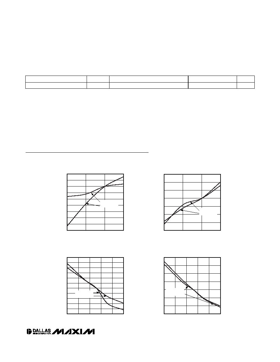
Typical Operating Characteristics
(V
CC
= 3.3V, T
A
= +25∞C, unless otherwise noted.)
PARAMETER
SYMBOL
CONDITIONS
MIN
TYP
MAX
UNITS
Input Capacitance
C
IN
5
10
pF
-2
-1
0
1
2
3
4
-3
CHANGE IN DELAY (%) vs. TEMPERATURE
DS1110L-250
DS1110L toc04
TEMPERATURE (
∞C)
CHANGE IN DELAY (%)
60
35
10
-15
-40
85
RISING EDGE
FALLING EDGE
CHANGE IN DELAY (%) vs. TEMPERATURE
DS1110L-500
DS1110L toc03
TEMPERATURE (
∞C)
CHANGE IN DELAY (%)
60
35
10
-15
-4
-3
-2
-1
0
1
2
3
4
5
6
-5
-40
85
RISING EDGE
FALLING EDGE
-0.3
-0.2
-0.1
0
0.1
0.2
0.3
-0.4
DELAY CHANGE (%)
vs. V
CC
DS1110L-250
DS1110L toc02
V
CC
(V)
CHANGE IN DELAY (%)
3.3
3.0
2.7
3.6
RAISING EDGE
FALLING EDGE
DELAY CHANGE (%)
vs. V
CC
DS1110L-500
DS1110L toc01
V
CC
(V)
CHANGE IN DELAY (%)
3.3
3.0
-0.30
-0.25
-0.20
-0.15
-0.10
-0.05
0
0.05
0.10
-0.35
2.7
3.6
RAISING EDGE
FALLING EDGE
DS1110L
3V 10-Tap Silicon Delay Line
4
______________________________________________________________________
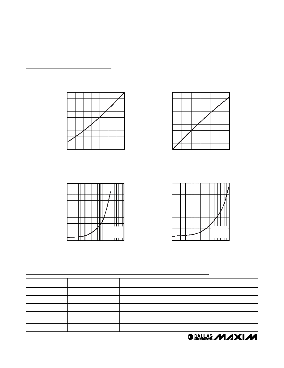
Typical Operating Characteristics (continued)
(V
CC
= 3.3V, T
A
= +25∞C, unless otherwise noted.)
1.0
5
10
15
20
25
0
0.1
10
ACTIVE CURRENT vs. INPUT FREQUENCY
DS1110L-500
DS1110L toc08
FREQUENCY (MHz)
CURRENT (mA)
V
CC
= 3.6V
15pF LOAD
ON EACH TAP
ACTIVE CURRENT vs. INPUT FREQUENCY
DS1110L-250
DS1110L toc07
FREQUENCY (MHz)
CURRENT (mA)
10
1
5
10
15
20
25
30
35
40
45
50
0
0.1
100
V
CC
= 3.6V
15pF LOAD
ON EACH TAP
DS1110L toc06
0.5
0.4
0.3
0.2
0.1
2.00E-03
4.00E-03
6.00E-03
8.00E-03
1.00E-02
1.20E-02
1.40E-02
1.60E-02
1.80E-02
0.00E+00
0
0.6
OUTPUT CURRENT LOW
vs. OUTPUT VOLTAGE LOW
OUTPUT VOLTAGE LOW (V)
OUTPUT CURRENT LOW (A)
V
CC
= 2.7V
OUTPUT CURRENT HIGH
vs. OUTPUT VOLTAGE HIGH
DS1110L toc05
OUTPUT VOLTAGE HIGH (V)
OUTPUT CURRENT HIGH (A)
2.6
2.5
2.3
2.4
2.2
2.1
-1.60E-02
-1.40E-02
-1.20E-02
-1.00E-02
-8.00E-03
-6.00E-03
-4.00E-03
-2.00E-03
0.00E+0
-1.80E-02
2.0
2.7
V
CC
= 2.7V
PIN
NAME
FUNCTION
1
IN
Input
2
N.C.
No Connection
7
GND
Ground
13, 3, 12, 4, 11,
5, 10, 6, 9, 8
Tap 1≠Tap 10
Tap Output Number
14
VCC
2.7V to 3.6V
Pin Description
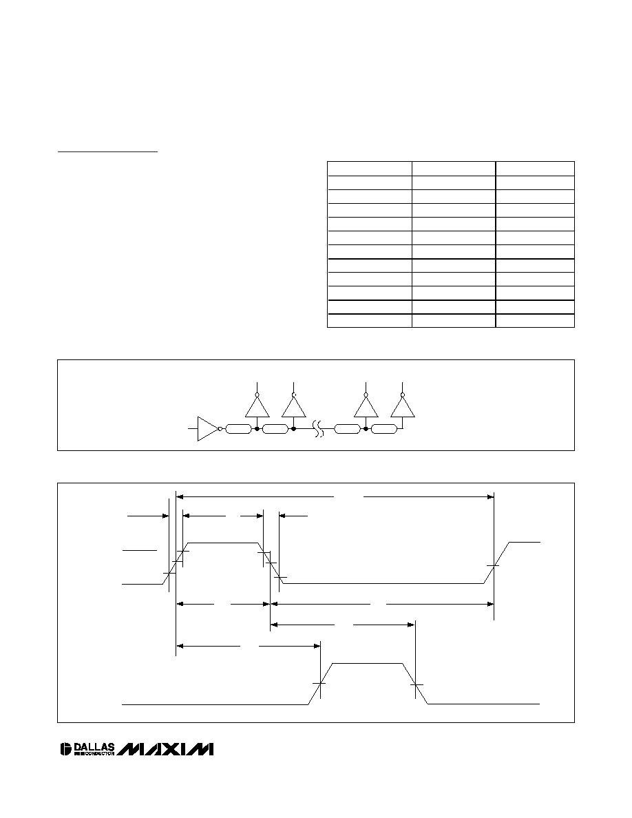
Detailed Description
The DS1110L 10-tap delay line is a 3V version of
the DS1110. It has 10 equally spaced taps providing
delays from 10ns to 500ns. The device is offered in a
standard 14-pin TSSOP. The DS1110L series delay lines
provide a nominal accuracy of ±5% or ±2ns, whichever is
greater, at 3.3V and +25∞C. The DS1110L is character-
ized to operate from 2.7V to 3.6V. The DS1110L repro-
duces the input-logic state at the tap 10 output after a
fixed delay as specified by the dash-number suffix of the
part number (
Table 1
). The DS1110L produces both lead-
ing- and trailing-edge delays with equal precision. Each
tap is capable of driving up to 10 74LS-type loads. Dallas
Semiconductor can customize standard products to meet
specific needs. Figure 1 is the DS1110_L logic diagram
and Figure 2 shows the timing diagram for the silicon
delay line.
DS1110L
3V 10-Tap Silicon Delay Line
_____________________________________________________________________
5
10%
10%
IN
TAP1
TAP2
TAP9
TAP10
10%
10%
Figure 1. Logic Diagram
PART
T O T A L D EL A Y ( n s ) DELAY/TAP
(ns)
DS1110LE-100
100
10
DS1110LE-125
125
12.5
DS1110LE-150
150
15
DS1110LE-175
175
17.5
DS1110LE-200
200
20
DS1110LE-250
250
25
DS1110LE-300
300
30
DS1110LE-350
350
35
DS1110LE-400
400
40
DS1110LE-450
450
45
DS1110LE-500
500
50
Table 1. Part Number by Delay (t
PHL
, t
PLH
)
V
IL
IN
OUT
0.6V
V
IH
t
RISE
2.4V
1.5V
1.5V
1.5V
1.5V
1.5V
0.6V
2.4V
PERIOD
t
WI
t
PLH
t
PLH
t
FALL
t
WI
Figure 2. Timing Diagram: Silicon Delay Line
DS1110L
Terminology
Period: The time elapsed between the leading edge of
the first pulse and the leading edge of the following pulse.
t
WI
(Pulse Width): The elapsed time on the pulse
between the 1.5V point on the leading edge and the
1.5V point on the trailing edge, or the 1.5V point on the
trailing edge and the 1.5V point on the leading edge.
t
RISE
(Input Rise Time): The elapsed time between the
20% and the 80% point on the leading edge of the
input pulse.
t
FALL
(Input Fall Time): The elapsed time between the
80% and the 20% point on the trailing edge of the input
pulse.
t
PLH
(Time Delay Rising): The elapsed time between
the 1.5V point on the leading edge of the input pulse
and the 1.5V point on the leading edge of any tap out-
put pulse.
t
PHL
(Time Delay, Falling): The elapsed time between
the 1.5V point on the trailing edge of the input pulse
and the 1.5V point on the trailing edge of any tap out-
put pulse.
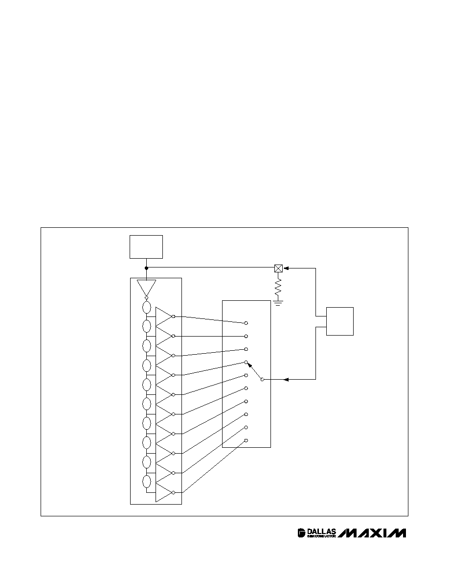
Test Setup Description
Figure 3
illustrates the hardware configuration used for
measuring the timing parameters on the DS1110L. A
precision pulse generator under software control pro-
duces the input waveform. Time delays are measured
by a time interval counter (20ps resolution) connected
3V 10-Tap Silicon Delay Line
6
______________________________________________________________________
PULSE
GENERATOR
TIME
INTERVAL
COUNTER
VHF SWITCH
CONTROL UNIT
STOP
DEVICE UNDER TEST
Z0 = 50
START
Figure 3. Test Circuit

DS1110L
3V 10-Tap Silicon Delay Line
Maxim cannot assume responsibility for use of any circuitry other than circuitry entirely embodied in a Maxim product. No circuit patent licenses are
implied. Maxim reserves the right to change the circuitry and specifications without notice at any time.
Maxim Integrated Products, 120 San Gabriel Drive, Sunnyvale, CA 94086 408-737-7600 _____________________ 7
© 2002 Maxim Integrated Products
Printed USA
is a registered trademark of Maxim Integrated Products.
between the input and each tap. Each tap is selected
and connected to the counter by a VHF switch-control
unit. All measurements are fully automated, with each
instrument controlled by a central computer over an
IEEE-488 bus.
Output
Each output is loaded with the equivalent of one 450
resistor in parallel with a 15pF capacitor. Delay is mea-
sured at the 1.5V level on the rising and falling edge.
INPUT
CONDITION
Ambient Temperature
+25∞C ±3∞C
Supply Voltage (V
CC
)
3.3V ±0.1V
High = 3.0V ±0.1V
Input Pulse
Low = 0.0V ±0.1V
Source Impedance
50
max
Rise and Fall Time
2ns max
Pulse Width
500ns (1µs for - 500ns)
Period
1µs (2µs for - 500ns)
Table 2. Test Conditions
Package Information
For the latest package outline information, go to www.maxim-ic.
com/packages.
Note: Above conditions are for test only and do not restrict the
operation of the device under other data sheet conditions.
Chip Information
TRANSISTOR COUNT: 6813