 | –≠–ª–µ–∫—Ç—Ä–æ–Ω–Ω—ã–π –∫–æ–º–ø–æ–Ω–µ–Ω—Ç: DS1202S-8 | –°–∫–∞—á–∞—Ç—å:  PDF PDF  ZIP ZIP |

DS1202, DS1202S
Serial Timekeeping Chip
DS1202, DS1202S
E
Copyright 1997 by Dallas Semiconductor Corporation.
All Rights Reserved. For important information regarding
patents and other intellectual property rights, please refer to
Dallas Semiconductor data books.
032697 1/11
FEATURES
∑
Real time clock counts seconds, minutes, hours, date
of the month, month, day of the week, and year with
leap year compensation valid up to 2100
∑
24 x 8 RAM for scratchpad data storage
∑
Serial I/O for minimum pin count
∑
2.0≠5.5 volt full operation
∑
Uses less than 300 nA at 2 volts
∑
Single≠byte or multiple≠byte (burst mode) data trans-
fer for read or write of clock or RAM data
∑
8≠pin DIP or optional 16≠pin SOIC for surface mount
∑
Simple 3≠wire interface
∑
TTL≠compatible (V
CC
= 5V)
∑
Optional industrial temperature range ≠40
∞
C to +85
∞
C
(IND)
ORDERING INFORMATION
DS1202
8≠pin DIP
DS1202S
16≠pin SOIC
DS1202S≠8
8≠pin SOIC
DS1202N
8≠pin DIP (IND)
DS1202SN
16≠pin SOIC (IND)
DS1202SN≠8 8≠pin SOIC (IND)
PIN ASSIGNMENT
1
2
3
4
5
6
7
8
16
15
14
13
12
11
10
9
NC
NC
X1
NC
X2
NC
NC
GND
V
CC
NC
SCLK
NC
I/O
NC
NC
RST
16≠PIN SOIC
8≠PIN DIP
V
CC
SCLK
I/O
RST
NC
X1
X2
GND
1
2
3
4
8
7
6
5
V
CC
SCLK
I/O
RST
NC
X1
X2
GND
1
2
3
4
8
7
6
5
8≠PIN SOIC
(208 mil)
PIN DESCRIPTION
NC
≠ No Connection
X1, X2
≠ 32.768 KHz Crystal Input
GND
≠ Ground
RST
≠ Reset
I/O
≠ Data Input/Output
SCLK
≠ Serial Clock
V
CC
≠ Power Supply Pin
DESCRIPTION
The DS1202 Serial Timekeeping Chip contains a real
time clock/calendar and 24 bytes of static RAM. It com-
municates with a microprocessor via a simple serial in-
terface. The real time clock/calendar provides seconds,
minutes, hours, day, date, month, and year information.
The end of the month date is automatically adjusted for
months with less than 31 days, including corrections for
leap year. The clock operates in either the 24≠hour or
12≠hour format with an AM/PM indicator. Interfacing the
DS1202 with a microprocessor is simplified by using
synchronous serial communication. Only three wires
are required to communicate with the clock/RAM: (1)
RST (Reset), (2) I/O (Data line), and (3) SCLK (Serial
clock). Data can be transferred to and from the clock/
RAM one byte at a time or in a burst of up to 24 bytes.
The DS1202 is designed to operate on very low power
and retain data and clock information on less than 1 mi-
crowatt.
DS1202, DS1202S
032697 2/11
OPERATION
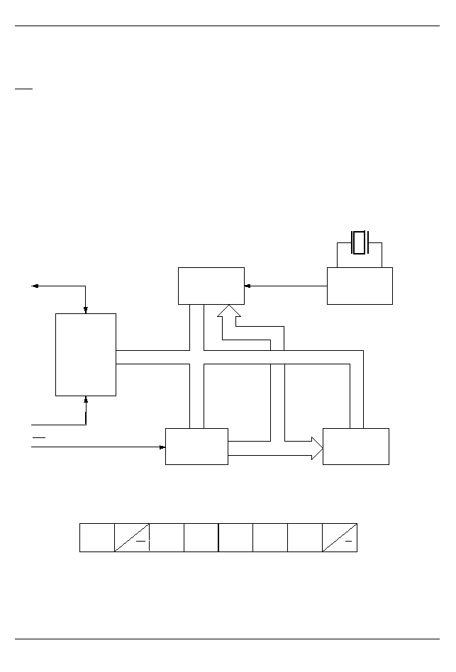
The main elements of the Serial Timekeeper are shown
in Figure 1: shift register, control logic, oscillator, real
time clock, and RAM. To initiate any transfer of data,
RST is taken high and eight bits are loaded into the shift
register providing both address and command informa-
tion. Data is serially input on the rising edge of the SCLK.
The first eight bits specify which of 32 bytes will be ac-
cessed, whether a read or write cycle will take place,
and whether a byte or burst mode transfer is to occur.
After the first eight clock cycles have occurred which
load the command word into the shift register, additional
clocks will output data for a read or input data for a write.
The number of clock pulses equals eight plus eight for
byte mode or eight plus up to 192 for burst mode.
COMMAND BYTE
The command byte is shown in Figure 2. Each data
transfer is initiated by a command byte. The MSB (Bit 7)
must be a logic 1. If it is zero, further action will be termi-
nated. Bit 6 specifies clock/calendar data if logic 0 or
RAM data if logic 1. Bits one through five specify the
designated registers to be input or output, and the LSB
(Bit 0) specifies a write operation (input) if logic 0 or read
operation (output) if logic 1. The command byte is al-
ways input starting with the LSB (bit 0).
DS1202 BLOCK DIAGRAM Figure 1
32.768 KHz
X2
X1
OSCILLATOR
AND DIVIDER
REAL TIME
CLOCK
DATA BUS
INPUT SHIFT
REGISTERS
COMMAND AND
CONTROL LOGIC
ADDRESS BUS
24 X 8 RAM
I/O
SCLK
RST
ADDRESS/COMMAND BYTE Figure 2
1
7
6
A4
5
A3
4
A2
3
A1
2
A0
1
RD
0
W
RAM
CK

DS1202, DS1202S
032697 3/11
RESET AND CLOCK CONTROL
All data transfers are initiated by driving the RST input
high. The RST input serves two functions. First, RST
turns on the control logic which allows access to the shift
register for the address/command sequence. Second,
the RST signal provides a method of terminating either
single byte or multiple byte data transfer. A clock cycle is
a sequence of a falling edge followed by a rising edge.
For data inputs, data must be valid during the rising
edge of the clock and data bits are output on t he falling
edge of clock. All data transfer terminates if the RST in-
put is low and the I/O pin goes to a high impedance
state. Data transfer is illustrated in Figure 3.
DATA INPUT
Following the eight SCLK cycles that input a write com-
mand byte, a data byte is input on the rising edge of the
next eight SCLK cycles. Additional SCLK cycles are ig-
nored should they inadvertently occur. Data is input
starting with bit 0. Due to the inherent nature of the logic
state machine, writing times containing an absolute
value of "59" seconds should be avoided.
DATA OUTPUT
Following the eight SCLK cycles that input a read com-
mand byte, a data byte is output on the falling edge of
the next eight SCLK cycles. Note that the first data bit to
be transmitted occurs on the first falling edge after the
last bit of the command byte is written. Additional SCLK
cycles retransmit the data bytes should they inadver-
tently occur so long as RST remains high. This opera-
tion permits continuous burst mode read capability.
Data is output starting with bit 0.
BURST MODE
Burst mode may be specified for either the clock/calen-
dar or the RAM registers by addressing location 31 deci-
mal (address/command bits one through five = logical
one). As before, bit six specified clock or RAM and bit 0
specifies read or write. There is no data storage capac-
ity at locations 8 through 31 in the Clock/Calendar Reg-
isters or locations 24 through 31 in the RAM registers.
When writing to the clock registers in the burst mode,
the first eight registers must be written in order for the
data to be transferred.
However, when writing to RAM in burst mode it is not
necessary to write all 24 bytes for the data to transfer.
Each byte that is written to will be transferred to RAM
regardless of whether all 24 bytes are written or not.
CLOCK/CALENDAR
The clock/calendar is contained in eight write/read reg-
isters as shown in Figure 4. Data contained in the clock/
calendar registers is in binary coded decimal format
(BCD).
CLOCK HALT FLAG
Bit 7 of the seconds register is defined as the clock halt
flag. When this bit is set to logic 1, the clock oscillator is
stopped and the DS1202 is placed into a low≠power
standby mode with a current drain of not more than 100
nanoamps. When this bit is written to logic 0, the clock
will start.
AM≠PM/12≠24 MODE
Bit 7 of the hours register is defined as the 12≠ or
24≠hour mode select bit. When high, the 12≠hour mode
is selected. In the 12≠hour mode, bit 5 is the AM/PM bit
with logic high being PM. In the 24≠hour mode, bit 5 is
the second 10 hour bit (20≠23 hours).
WRITE PROTECT BIT
Bit 7 of the control register is the write protect bit. The
first seven bits (bits 0≠6) are forced to zero and will al-
ways read a zero when read. Before any write operation
to the clock or RAM, bit 7 must be zero. When high, the
write protect bit prevents a write operation to any other
register.
CLOCK/CALENDAR BURST MODE
The clock/calendar command byte specifies burst
mode operation. In this mode the eight clock/calendar
registers can be consecutively read or written (see Fig-
ure 4) starting with bit 0 of address 0.
RAM
The static RAM is 24 x 8 bytes addressed consecutively
in the RAM address space.
RAM BURST MODE
The RAM command byte specifies burst mode opera-
tion. In this mode, the 24 RAM registers can be consec-
utively read or written (see Figure 4) starting with bit 0 of
address 0.

DS1202, DS1202S
032697 4/11
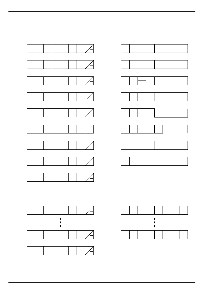
REGISTER SUMMARY
A register data format summary is shown in Figure 4.
CRYSTAL SELECTION
A 32.768 KHz crystal, can be directly connected to the
DS1202 via pins 2 and 3 (X1, X2). The crystal selected
for use should have a specified load capacitance (CL) of
6 pF. The crystal is connected directly to the X1 and X2
pins. There is no need for external capacitors or resis-
tors. Note: X1 and X2 are very high impedance nodes.
It is recommended that they and the crystal be guard≠
ringed with ground and that high frequency signals be
kept away from the crystal area. For more information
on crystal selection and crystal layout considerations,
please consult Application Note 58, "Crystal Consider-
ations with Dallas Real Time Clocks".
DATA TRANSFER SUMMARY Figure 3
SCLK
I/O
RST
0
1
2
3
4
5
6
7
0
1
2
3
4
5
6
7
R/W
A0
A1
A2
A3
A4
1
ADDRESS COMMAND
DATA INPUT/OUTPUT
SINGLE BYTE TRANSFER
SCLK
I/O
0
1
2
3
4
5
6
7
0
1
2
4
5
6
7
1
1
1
1
1
1
ADDRESS COMMAND
DATA I/O BYTE N
BURST MODE TRANSFER
RST
R/W
DATA I/O BYTE 1
R/C
R/C
FUNCTION
BYTE N
SCLK n
CLOCK
8
72
RAM
24
200
DS1202, DS1202S
032697 5/11
REGISTER ADDRESS/DEFINITION Figure 4
1
7
6
0
5
0
4
0
3
0
2
0
1
RD
0
W
REGISTER ADDRESS
REGISTER DEFINITION
0
1
0
0
0
0
1
RD
0
W
1
0
0
0
1
0
RD
0
1
0
0
0
1
1
RD
0
W
W
1
0
0
1
0
0
RD
0
1
0
0
1
0
1
RD
0
1
0
0
1
1
0
RD
0
1
0
0
1
1
1
RD
0
W
W
W
W
1
1
1
1
1
1
RD
0
W
1
0
0
0
0
0
RD
1
1
1
0
1
1
1
RD
1
1
1
1
1
1
1
RD
1
W
W
W
A. CLOCK
B. RAM
SEC
MIN
HR
DATE
MONTH
DAY
YEAR
CONTROL
CLOCK
BURST
CH
SEC
10 SEC
0
12/
HR
HR
0
0
10 DATE
0
0
0
10
0
0
0
0
0
10 YEAR
WP
00≠59
00≠59
01≠12
01≠28/29
01≠12
01≠07
0≠99
RAM 0
RAM 23
RAM
BURST
RAM DATA 0
RAM DATA 23
MIN
10 MIN
00≠23
24
10
A/P
01≠30
01≠31
DATE
M
MONTH
YEAR
DAY
0
FORCED TO ZERO