1 of 6
111899
FEATURES
Converts CMOS RAMs into nonvolatile
memories
Unconditionally write protects when V
CC
is
out of tolerance
Automatically switches to battery when
power-fail occurs
Space saving 8-pin DIP
Consumes less than 100 nA of battery current
Tests battery condition on power up
Provides for redundant batteries
Optional 5% or 10% power-fail detection
Low forward voltage drop on the V
CC
switch
Optional 16-pin SOIC surface mount package
Optional industrial temperature range of
-40�C to +85�C
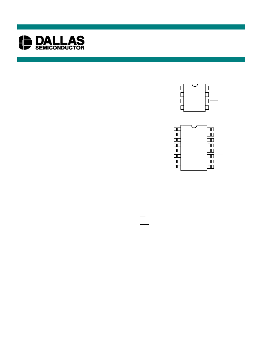
PIN ASSIGNMENT
PIN DESCRIPTION
V
CCO
- RAM Supply
V
BAT1
- + Battery 1
TOL
- Power Supply Tolerance
GND
- Ground
CE
- Chip Enable Input
CEO
- Chip Enable Output
V
BAT2
- + Battery 2
V
CCI
- + Supply
NC
- No Connect
DESCRIPTION
The DS1210 Nonvolatile Controller Chip is a CMOS circuit which solves the application problem of
converting CMOS RAM into nonvolatile memory. Incoming power is monitored for an out-of-tolerance
condition. When such a condition is detected, chip enable is inhibited to accomplish write protection and
the battery is switched on to supply the RAM with uninterrupted power. Special circuitry uses a low-
leakage CMOS process which affords precise voltage detection at extremely low battery consumption.
The 8-pin DIP package keeps PC board real estate requirements to a minimum. By combining the
DS1210 Nonvolatile Controller Chip with a CMOS memory and batteries, nonvolatile RAM operation
can be achieved.
DS1210
Nonvolatile Controller Chip
www.dalsemi.com
VCCO
VBAT1
TOL
GND
1
2
3
4
VCCI
VBAT2
CEO
CE
8
7
6
5
DS1210 8-pin DIP (300-mil)
See Mech. Drawings Section
NC
VCCO
NC
VBAT1
NC
TOL
NC
GND
NC
VCCI
NC
VBAT2
NC
CEO
NC
CE
1
2
3
4
5
6
7
8
16
15
14
13
12
11
10
9
DS1210S 16-pin SOIC (300-mil)
See Mech. Drawings Section

DS1210
2 of 6
OPERATION
The DS1210 nonvolatile controller performs five circuit functions required to battery back up a RAM.
First, a switch is provided to direct power from the battery or the incoming supply (V
CCI
) depending on
which is greater. This switch has a voltage drop of less than 0.3V. The second function which the
nonvolatile controller provides is power-fail detection. The DS1210 constantly monitors the incoming
supply. When the supply goes out of tolerance a precision comparator detects power-fail and inhibits chip
enable (
CEO
). The third function of write protection is accomplished by holding the
CEO
output signal to
within 0.2 volts of the V
CCI
or battery supply. If
CE
input is low at the time power-fail detection occurs,
the
CEO
output is kept in its present state until
CE
is returned high. The delay of write protection until
the current memory cycle is completed prevents the corruption of data. Power-fail detection occurs in the
range of 4.75 volts to 4.5 volts with the tolerance Pin 3 grounded. If Pin 3 in connected to V
CCO
, then
power-fail detection occurs in the range of 4.5 volts to 4.25 volts. During nominal supply conditions
CEO
will follow
CE
with a maximum propagation delay of 20ns. The fourth function the DS1210
performs is a battery status warning so that potential data loss is avoided. Each time that the circuit is
powered up the battery voltage is checked with a precision comparator. If the battery voltage is less than
2.0 volts, the second memory cycle is inhibited. Battery status can, therefore, be determined by
performing a read cycle after power-up to any location in memory, verifying that memory location
content. A subsequent write cycle can then be executed to the same memory location altering the data. If
the next read cycle fails to verify the written data, then the batteries are less than 2.0V and data is in
danger of being corrupted. The fifth function of the nonvolatile controller provides for battery
redundancy. In many applications, data integrity is paramount. In these applications it is often desirable to
use two batteries to ensure reliability. The DS1210 controller provides an internal isolation switch which
allows the connection of two batteries. During battery backup operation the battery with the highest
voltage is selected for use. If one battery should fail, the other will take over the load. The switch to a
redundant battery is transparent to circuit operation and to the user. A battery status warning will occur
when the battery in use falls below 2.0 volts. A grounded V
BAT2
pin will not activate a battery-fail
warning. In applications where battery redundancy is not required, a single battery should be connected to
the BAT1 pin. The BAT2 battery pin must be grounded. The nonvolatile controller contains circuitry to
turn off the battery backup. This is to maintain the battery(s) at its highest capacity until the equipment is
powered up and valid data is written to the SRAM. While in the freshness seal mode the
CEO
and V
CCO
will be forced to V
OL
. When the batteries are first attached to one or both of the V
BAT
pins, V
CCO
will not
provide battery back-up until V
CCI
exceeds V
CCTP
, as set by the T
OL
pin, and then falls below V
BAT
.
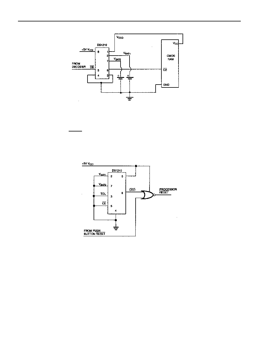
Figure 1 shows a typical application incorporating the DS1210 in a microprocessor-based system. Section
A shows the connections necessary to write protect the RAM when V
CC
is less than 4.75 volts and to back
up the supply with batteries. Section B shows the use of the DS1210 to halt the processor when V
CC
is
less than 4.75 volts and to delay its restart on power-up to prevent spurious writes.

DS1210
3 of 6
SECTION A - BATTERY BACKUP Figure 1
BATTERY BACKUP CURRENT DRAIN EXAMPLE
CONSUMPTION
DS1210 I
BAT
100 nA
RAM I
CC02
10
�
A
Total Drain
10.1
�
A
SECTION B - PROCESSOR RESET

DS1210
4 of 6
ABSOLUTE MAXIMUM RATINGS*
Voltage on Any Pin Relative to Ground
-0.3V to +7.0V
Operating Temperature
0
�
C to 70
�
C
Storage Temperature
-55
�
C to +125
�
C
Soldering Temperature
260
�
C for 10 seconds
*
This is a stress rating only and functional operation of the device at these or any other conditions
above those indicated in the operation sections of this specification is not implied. Exposure to
absolute maximum rating conditions for extended periods of time may affect reliability.
RECOMMENDED DC OPERATING CONDITIONS
(0
�
C to 70
�
C)
PARAMETER
SYMBOL
MIN
TYP
MAX
UNITS
NOTES
Pin 3 = GND Supply Voltage
V
CCI
4.75
5.0
5.5
V
1
Pin 3 = V
CCO
Supply Voltage
V
CCI
4.5
5.0
5.5
V
1
Logic 1 Input
V
IH
2.2
V
CC
+0.3
V
1
Logic 0 Input
V
IL
-0.3
+0.8
V
1
Battery Input
V
BAT1
,
V
BAT2
2.0
4.0
V
1, 2
(0
�
C to 70
�
C; V
CCI
= 4.75 to 5.5V PIN 3 = GND)
DC ELECTRICAL CHARACTERISTICS
(V
CCI
= 4.5 to 5.5V, PIN 3 = V
CCO
)
PARAMETER
SYMBOL
MIN
TYP
MAX
UNITS
NOTES
Supply Current
I
CCI
5
mA
3
Supply Voltage
V
CCO
V
CC
-0.2
V
1
Supply Current
I
CCO1
80
mA
4
Input Leakage
I
IL
-1.0
+1.0
�A
Output Leakage
I
LO
-1.0
+1.0
�A
CEO
Output @ 2.4V
I
OH
-1.0
mA
5
CEO
Output @ 0.4V
I
OL
4.0
mA
5
V
CC
Trip Point (TOL=GND)
V
CCTP
4.50
4.62
4.74
V
1
V
CC
Trip Point (TOL=V
CCO
)
V
CCTP
4.25
4.37
4.49
V
1
(0�C to 70�C; V
CCI
= < V
BAT
)
CEO
Output
V
OHL
V
BAT
-0.2
V
7
V
BAT1
or V
BAT2
Battery Current
I
BAT
100
nA
2, 3
Battery Backup Current
@ V
CCO
= V
BAT
� 0.3V
I
CCO2
50
�A
6, 7

DS1210
5 of 6
CAPACITANCE
(T
A
= 25�C)
PARAMETER
SYMBOL
MIN
TYP
MAX
UNITS
NOTES
Input Capacitance
C
IN
5
pF
Output Capacitance
C
OUT
7
pF
(0�C to 70�C; V
CCI
= 4.75V to 5.5V, PIN 3 = GND)
AC ELECTRICAL CHARACTERISTICS
(V
CCI
= 4.75V to 5.5V, PIN 3 = GND)
PARAMETER
SYMBOL
MIN
TYP
MAX
UNITS
NOTES
CE
Propagation Delay
t
PD
5
10
20
ns
5
CE
High to Power-Fail
t
PF
0
ns
(0�C to 70�C; V
CCI
= 4.75V, PIN 3 = GND; V
CCI
< 4.5, PIN 3 = V
CCO
)
Recovery at Power Up
t
REC
2
80
125
ms
V
CC
Slew Rate Power-Down
t
F
300
�s
V
CC
Slew Rate Power-Down
t
FB
10
�s
V
CC
Slew Rate Power-Down
t
R
0
�s
CE
Pulse Width
t
CE
1.5
�s
8
NOTES:
1.
All voltages are referenced to ground.
2.
Only one battery input is required. Unused battery inputs must be grounded.
3.
Measured with V
CCO
and
CEO
open.
4.
I
CC01
is the maximum average load which the DS1210 can supply to the memories.
5.
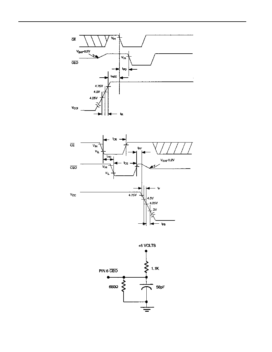
Measured with a load as shown in Figure 2.
6.
I
CC02
is the maximum average load current which the DS1210 can supply to the memories in the
battery backup mode.
7.
t
CE
max. must be met to ensure data integrity on power loss.
8.
CEO
can only sustain leakage current in the battery backup mode.

DS1210
6 of 6
TIMING DIAGRAM: POWER-UP
TIMING DIAGRAM: POWER-DOWN
OUTPUT LOAD Figure 2
