1 of 4
111899
FEATURES
Provides bank switching for 16 banks of
memory
Bank switching is software-controlled by a
pattern recognition sequence on four address
inputs
Automatically sets all 16 banks off on
power-up
Bank switching logic allows only one bank on
at a time
Custom recognition patterns are available to
prevent unauthorized access
Full
±
10% operating range
Low-power CMOS circuitry
Can be used to expand the address range of
microprocessors and decoders
Optional 16-pin SOIC surface mount package
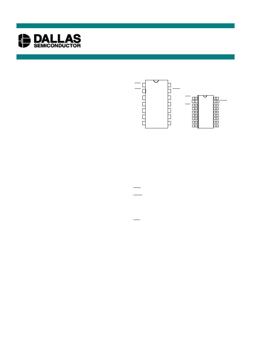
PIN ASSIGNMENT
PIN DESCRIPTION
A
W
-A
Z
- Address Inputs
CEI
- Chip Enable Input
CEO
- Chip Enable Output
NC
- No Connection
BS1,BS2,
- Bank Select Outputs
BS3,BS4
- Bank Select Outputs
I
PF
- Power Fail Input
V
CC
- +5 Volts
GND -
Ground
DESCRIPTION
The DS1222 BankSwitch Chip is a CMOS circuit designed to select one of 16 memory banks under
software control. Memory bank switching allows for an increase in memory capacity without additional
address lines. Continuous blocks of memory are enabled by selecting proper memory bank through a
pattern recognition sequence on four address inputs. Custom patterns from Dallas Semiconductor can
provide security through uniqueness and prevent unauthorized access. By combining the DS1222 with
the DS1212 Nonvolatile Controller x16 Chip, up to 16 banks of static RAMs can be selected.
DS1222
BankSwitch Chip
www.dalsemi.com
DS1222 14-Pin DIP
(300-mil)
See Mech. Drawings
Section
CEI
V
CC
13
AW
AY
GND
CEO
BS1
BS2
BS3
BS4
NC
1
2
3
4
5
6
7
14
12
11
10
9
8
PFI
AX
AZ
16
15
14
13
12
11
10
9
1
2
3
4
5
6
7
8
V
CC
CEO
NC
BS1
BS2
BS3
NC
BS4
CEI
NC
PFI
AW
AX
AY
AZ
GND
DS1222S 16-Pin SOIC
(300-mil)
See Mech. Drawings
Section
DS1222
2 of 4
OPERATION - BANK SWITCHING
Initially, on power-up all four bank select outputs are low and the chip enable output (
CEO
) is held high.
(Note: the power fail input [
I
F
P
] must be low prior to power-up to assure proper initialization.) Bank
switching is achieved by matching a predefined pattern stored within the DS1222 with a 16-bit sequence
received on four address inputs. Prior to entering the 16-bit pattern, which sets the bank switch, a read
cycle of 1111 on address inputs AW through AZ should be executed to guarantee that pattern entry starts
with bit 0. Each set of address inputs is clocked into the DS1222 when
CEI
is driven low. All 16 inputs
must be consecutive read cycles. The first eleven cycles must match the exact bit pattern as shown in
Table 1. The last five cycles must match the exact bit pattern as shown for addresses AX, AY, and AZ.
However, address line AW defines the bank number to be enabled as per Table 2.
Switching to a selected bank of memory occurs on the rising edge of
CEI
when the last set of bits is input
and a match has been established. After bank selection
CEO
always follows
CEI
with a maximum
propagation delay of 15 ns. The bank selected is determined by the levels set on Bank Select 1 through
Bank Select 4 as per Table 2. These levels are held constant for all memory cycles until a new memory
bank is selected.
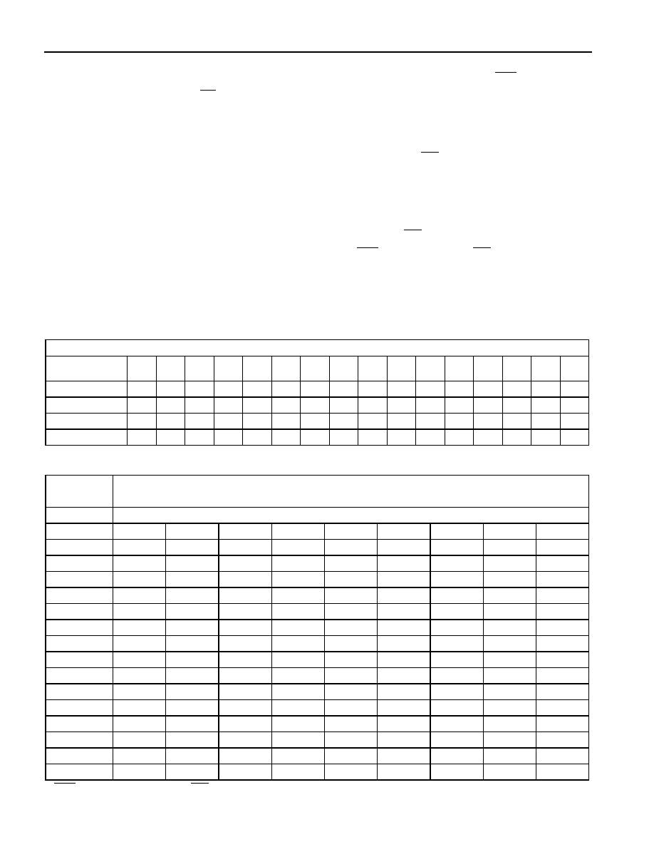
ADDRESS BIT SEQUENCE Table 1
BIT SEQUENCE
ADDRESS
INPUTS
0
1
2
3
4
5
6
7
8
9
10
11
12
13
14
15
A
W
1
0
1
0
0
0
1
1
0
1
0
x
x
x
x
x
A
X
0
1
0
1
1
1
0
0
1
0
1
0
0
0
1
1
A
Y
1
0
1
0
0
0
1
1
0
1
0
1
1
1
0
0
A
Z
0
1
0
1
1
1
0
0
1
0
1
0
0
0
1
1
X See Table 2
BANK SELECT CONTROL Table 2
A
W
Bit Sequence
Outputs
Bank
Selected
11
12
13
14
15
BS1
BS2
BS3
BS4
*Banks Off
0
X
X
X
X
Low
Low
Low
Low
Bank 0
1
0
0
0
0
Low
Low
Low
Low
Bank 1
1
0
0
0
1
High
Low
Low
Low
Bank 2
1
0
0
1
0
Low
High
Low
Low
Bank 3
1
0
0
1
1
High
High
Low
Low
Bank 4
1
0
1
0
0
Low
Low
High
Low
Bank 5
1
0
1
0
1
High
Low
High
Low
Bank 6
1
0
1
1
0
Low
High
High
Low
Bank 7
1
0
1
1
1
High
High
High
Low
Bank 8
1
1
0
0
0
Low
Low
Low
High
Bank 9
1
1
0
0
1
High
Low
Low
High
Bank 10
1
1
0
1
0
Low
High
Low
High
Bank 11
1
1
0
1
1
High
High
Low
High
Bank 12
1
1
1
0
0
Low
Low
Low
High
Bank 13
1
1
1
0
1
High
Low
High
High
Bank 14
1
1
1
1
0
Low
High
High
High
Bank 15
1
1
1
1
1
High
High
High
High
*
CEO
=V
IH
independent of
CEI
DS1222
3 of 4
ABSOLUTE MAXIMUM RATINGS*
Voltage on any Pin Relative to Ground
-0.3V to +7.0V
Operating Temperature
0
∞
C to 70
∞
C
Storage Temperature
-55
∞
C to +125
∞
C
This is a stress rating only and functional operation of the device at these or any other conditions
above those indicated in the operation sections of this specification is not implied. Exposure to
absolute maximum rating conditions for extended periods of time may affect reliability.
RECOMMENDED DC OPERATING CONDITIONS
(0
∞
C to 70
∞
C)
PARAMETER
SYMBOL
MIN
TYP
MAX
UNITS
NOTES
Power Supply Voltage
V
CC
4.5
5.0
5.5
V
1
Logic 1
V
IH
2.2
V
CC
+0.3
V
1
Logic 0
V
IL
-0.3
+0.8
V
1
DC ELECTRICAL CHARACTERISTICS
(0
∞
C to 70
∞
C; V
CC
= 5V
±
10%)
PARAMETER
SYMBOL
MIN
TYP
MAX
UNITS
NOTES
Input Leakage Current
I
IL
-1.0
+1.0
µ
A
I/O Leakage Current
I
LO
-1.0
+1.0
µ
A
Output Current @ 2.4V
I
OH
-1.0
mA
2
Output Current @ 0.4V
I
OL
+4.0
mA
2
Operating Current
I
CC
15
mA
CAPACITANCE
(T
A
= 25
∞
C)
PARAMETER
SYMBOL
MIN
TYP
MAX
UNITS
NOTES
Input Capacitance
C
IN
5
10
pF
Input/Output Capacitance
C
I/O
5
10
pF
AC ELECTRICAL CHARACTERISTICS
(0
∞
C to 70
∞
C; V
CC
= 5V
±
10%)
PARAMETER
SYMBOL
MIN
TYP
MAX
UNITS
NOTES
Address Setup
t
AS
5
ns
Address Hold
t
AH
50
ns
Read Recovery
t
RR
40
ns
Propagation Delay
t
PD
15
ns
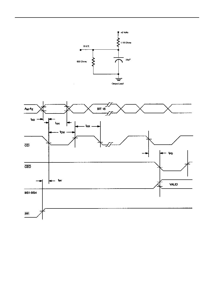
2
Power Fail Input to First
CEI
t
PF
50
ns
Chip Enable Low
t
CW
110
ns
NOTES:
1.
All voltages are referenced to ground.
2.
Measured with a load as shown in Figure 1.