E
Copyright 1997 by Dallas Semiconductor Corporation.
All Rights Reserved. For important information regarding
patents and other intellectual property rights, please refer to
Dallas Semiconductor data books.
DS1244Y
256K NV SRAM with Phantom Clock
DS1244Y
032697 1/12
FEATURES
∑
Real time clock keeps track of hundredths of seconds,
minutes, hours, days, date of the month, months, and
years
∑
32K x 8 NV SRAM directly replaces volatile static
RAM or EEPROM
∑
Embedded lithium energy cell maintains calendar op-
eration and retains RAM data
∑
Watch function is transparent to RAM operation
∑
Month and year determine the number of days in each
month; volid up to 1200
∑
Standard 28≠pin JEDEC pinout
∑
Full 10% operating range
∑
Operating temperature range 0
∞
C to 70
∞
C
∑
Accuracy is better than
±
1 minute/month @ 25
∞
C
∑
Over 10 years of data retention in the absence of
power
∑
Available in 120, 150 and 200 ns access time
ORDERING INFORMATION
DS1244Y≠XXX
DS1244Y
≠120
120 ns access
≠150
150 ns access
200 ns access
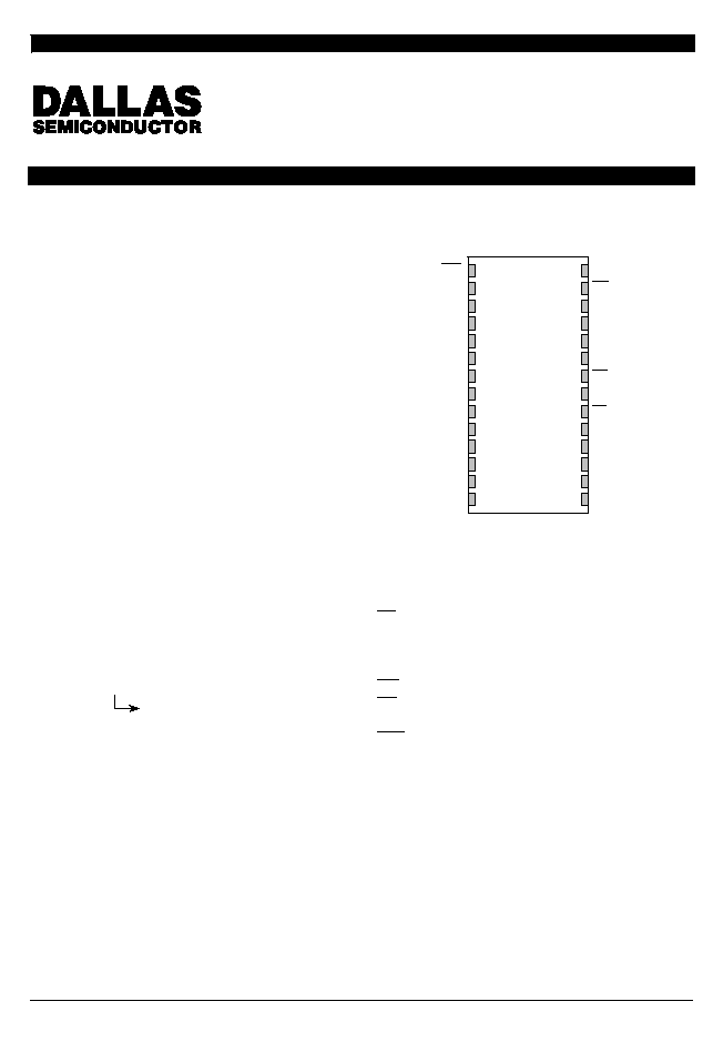
PIN ASSIGNMENT
28≠PIN ENCAPSULATED PACKAGE
740 MIL EXTENDED
V
CC
WE
A13
A8
A9
A11
OE
A10
CE
DQ7
DQ6
DQ5
DQ4
DQ3
A14/RST
A12
A7
A6
A5
A4
A3
A2
A1
A0
DQ0
DQ1
DQ2
GND
1
2
3
4
5
6
7
8
9
10
11
12
13
14
28
27
26
25
24
23
22
21
20
19
18
17
16
15
PIN DESCRIPTION
A
o
≠A
14
≠ Address Inputs
CE
≠ Chip Enable
GND
≠ Ground
DQ
0-
DQ
7
≠ Data In/Data Out
V
CC
≠ Power (+5V)
WE
≠ Write Enable
OE
≠ Output Enable
NC
≠ No Connect
RST
≠ Reset
DESCRIPTION
The DS1244Y 256K NV SRAM with Phantom Clock is a
fully static nonvolatile RAM (organized as 32,768 words
by 8 bits) with a built≠in real time clock. The DS1244Y
has a self≠contained lithium energy source and control
circuitry which constantly monitors V
CC
for an out≠of≠
tolerance condition. When such a condition occurs, the
lithium energy source is automatically switched on and
write protection is unconditionally enabled to prevent
garbled data in both the memory and real time clock.
The Phantom Clock provides timekeeping information
including hundredths of seconds, seconds, minutes,
hours, day, date, month, and year information. The date
at the end of the month is automatically adjusted for
months with less than 31 days, including correction for
leap years. The Phantom Clock operates in either
24≠hour or 12≠hour format with an AM/PM indicator.

DS1244Y
032697 2/12
RAM READ MODE
The DS1244Y executes a read cycle whenever WE
(Write Enable) is inactive (high) and CE (Chip Enable) is
active (low). The unique address specified by the 15 ad-
dress inputs (A0-A14) defines which of the 32,768 bytes
of data is to be accessed. Valid data will be available to
the eight data output drivers within t
ACC
(Access Time)
after the last address input signal is stable, providing
that CE and OE (Output Enable) access times and
states are also satisfied. If OE and CE access times are
not satisfied, then data access must be measured from
the later occurring signal (CE or OE) and the limiting pa-
rameter is either t
CO
for CE or t
OE
for OE rather than ad-
dress access.
RAM WRITE MODE
The DS1244Y is in the write mode whenever the WE
and CE signals are in the active (low) state after address
inputs are stable. The latter occurring falling edge of CE
or WE will determine the start of the write cycle. The
write cycle is terminated by the earlier rising edge of CE
or WE. All address inputs must be kept valid throughout
the write cycle. WE must return to the high state for a
minimum recovery time (t
WR
) before another cycle can
be initiated. The OE control signal should be kept inac-
tive (high) during write cycles to avoid bus contention.
However, if the output bus has been enabled (CE and
OE active) then WE will disable the outputs in t
ODW
from
its falling edge.
DATA RETENTION MODE
The DS1244Y provides full functional capability for V
CC
greater than 4.5 volts and write protects by approxi-
mately 4.0 volts. Data is maintained in the absence of
V
CC
without any additional support circuitry. The non-
volatile static RAM constantly monitors V
CC
. Should the
supply voltage decay, the RAM automatically write pro-
tects itself. All inputs to the RAM become "don't care"
and all outputs are high impedance. As V
CC
falls below
approximately 3.0 volts, the power switching circuit con-
nects the lithium energy source to RAM to retain data.
During power≠up, when V
CC
rises above approximately
3.0 volts, the power switching circuit connects external
V
CC
to the RAM and disconnects the lithium energy
source. Normal RAM operation can resume after V
CC
exceeds 4.5 volts.
PHANTOM CLOCK OPERATION
Communication with the Phantom Clock is established
by pattern recognition on a serial bit stream of 64 bits
which must be matched by executing 64 consecutive
write cycles containing the proper data on DQ0. All ac-
cesses which occur prior to recognition of the 64≠bit pat-
tern are directed to memory.
After recognition is established, the next 64 read or write
cycles either extract or update data in the Phantom
Clock, and memory access is inhibited.
Data transfer to and from the timekeeping function is ac-
complished with a serial bit stream under control of Chip
Enable (CE), Output Enable (OE), and Write Enable
(WE). Initially, a read cycle to any memory location us-
ing the CE and OE control of the Phantom Clock starts
the pattern recognition sequence by moving a pointer to
the first bit of the 64≠bit comparison register. Next, 64
consecutive write cycles are executed using the CE and
WE control of the SmartWatch. These 64 write cycles
are used only to gain access to the Phantom Clock.
Therefore, any address to the memory in the socket is
acceptable. However, the write cycles generated to
gain access to the Phantom Clock are also writing data
to a location in the mated RAM. The preferred way to
manage this requirement is to set aside just one ad-
dress location in RAM as a Phantom Clock scratch pad.
When the first write cycle is executed, it is compared to
bit 0 of the 64≠bit comparison register. If a match is
found, the pointer increments to the next location of the
comparison register and awaits the next write cycle. If a
match is not found, the pointer does not advance and all
subsequent write cycles are ignored. If a read cycle oc-
curs at any time during pattern recognition, the present
sequence is aborted and the comparison register point-
er is reset. Pattern recognition continues for a total of 64
write cycles as described above until all the bits in the
comparison register have been matched (this bit pattern
is shown in Figure 1). With a correct match for 64 bits,
the Phantom Clock is enabled and data transfer to or
from the timekeeping registers can proceed. The next
64 cycles will cause the Phantom Clock to either receive
or transmit data on DQ0, depending on the level of the
OE pin or the WE pin. Cycles to other locations outside
the memory block can be interleaved with CE cycles
without interrupting the pattern recognition sequence or
data transfer sequence to the Phantom Clock.
DS1244Y
032697 3/12
PHANTOM CLOCK
REGISTER INFORMATION
The Phantom Clock information is contained in 8 regis-
ters of 8 bits, each of which is sequentially accessed one
bit at a time after the 64≠bit pattern recognition se-
quence has been completed. When updating the Phan-
tom Clock registers, each register must be handled in
groups of 8 bits. Writing and reading individual bits with-
in a register could produce erroneous results. These
read/write registers are defined in Figure 2.
Data contained in the Phantom Clock register is in
binary coded decimal format (BCD). Reading and writ-
ing the registers is always accomplished by stepping
through all 8 registers, starting with bit 0 of register 0 and
ending with bit 7 of register 7.
PHANTOM CLOCK REGISTER DEFINITION Figure 1
7
6
5
4
3
2
1
0
1
1
0
0
0
1
0
1
0
0
1
1
1
0
1
0
1
0
1
0
0
0
1
1
0
1
0
1
1
1
0
0
1
1
0
0
0
1
0
1
0
0
1
1
1
0
1
0
1
0
1
0
0
0
1
1
0
1
0
1
1
1
0
0
C5
3A
A3
5C
C5
3A
A3
5C
BYTE 0
BYTE 1
BYTE 2
BYTE 3
BYTE 4
BYTE 5
BYTE 6
BYTE 7
HEX
VALUE
NOTE:
The pattern recognition in Hex is C5, 3A, A3, 5C, C5, 3A, A3, 5C. The odds of this pattern being accidentally dupli-
cated and causing inadvertent entry to the Phantom Clock is less than 1 in 10
19
. This pattern is sent to the Phantom
Clock LSB to MSB.

DS1244Y
032697 4/12
PHANTOM CLOCK REGISTER DEFINITION Figure 2
7
6
5
4
3
2
1
0
0.1 SEC
00≠99
00≠59
00≠59
01≠12
01≠07
01≠31
01≠12
00≠99
0
1
2
3
4
5
6
7
RANGE
(BCD)
REGISTER
0
0
12/24
0
10
HR
0
0
0
0
0
0
0
0
10
MONTH
10 YEAR
YEAR
0.01 SEC
00≠23
10 SEC
SECONDS
10 MIN
MINUTES
A/P
HOUR
OSC
RST
DAY
10 DATE
DATE
MONTH
AM≠PM/12/24 MODE
Bit 7 of the hours register is defined as the 12≠ or
24≠hour mode select bit. When high, the 12≠hour mode
is selected. In the 12≠hour mode, bit 5 is the AM/PM bit
with logic high being PM. In the 24≠hour mode, bit 5 is
the second 10≠hour bit (20≠23 hours).
OSCILLATOR AND RESET BITS
Bits 4 and 5 of the day register are used to control the
RESET and oscillator functions. Bit 4 controls the
RESET (pin 1). When the RESET bit is set to logic 1, the
RESET input pin is ignored. When the RESET bit is set
to logic 0, a low input on the RESET pin will cause the
Phantom Clock to abort data transfer without changing
data in the watch registers. Bit 5 controls the oscillator.
When set to logic 1, the oscillator is off. When set to log-
ic 0, the oscillator turns on and the watch becomes op-
erational. These bits are shipped from the factory set to
a logic 1.
ZERO BITS
Registers 1, 2, 3, 4, 5, and 6 contain one or more bits
which will always read logic 0. When writing these loca-
tions, either a logic 1 or 0 is acceptable.

DS1244Y
032697 5/12
ABSOLUTE MAXIMUM RATINGS*
Voltage on Any Pin Relative to Ground
≠0.3V to +7.0V
Operating Temperature
0
∞
C to 70
∞
C
Storage Temperature
≠40
∞
C to +70
∞
C
Soldering Temperature
260
∞
C for 10 seconds (See Note 13)
* This is a stress rating only and functional operation of the device at these or any other conditions above those
indicated in the operation sections of this specification is not implied. Exposure to absolute maximum rating
conditions for extended periods of time may affect reliability.
RECOMMENDED DC OPERATING CONDITIONS
(0
∞
C to 70
∞
C)
PARAMETER
SYMBOL
MIN
TYP
MAX
UNITS
NOTES
Power Supply Voltage
V
CC
4.5
5.0
5.5
V
Input Logic 1
V
IH
2.2
V
CC
+0.3
V
Input Logic 0
V
IL
0.3
0.8
V
DC ELECTRICAL CHARACTERISTICS
(0
∞
C to 70
∞
C; V
CC
= 5V
±
10%)
PARAMETER
SYMBOL
MIN
TYP
MAX
UNITS
NOTES
Input Leakage Current
I
IL
≠1.0
+1.0
µ
A
12
I/O Leakage Current
CE
V
IH
V
CC
I
IO
≠1.0
+1.0
µ
A
Output Current @ 2.4V
I
OH
≠1.0
mA
Output Current @ 0.4V
I
OL
2.0
mA
Standby Current CE = 2.2V
I
CCS1
5.0
10
mA
Standby Current CE = V
CC
≠ 0.5V
I
CCS2
3.0
5.0
mA
Operating Current t
CYC
= 200 ns
I
CC01
85
mA
DC TEST CONDITIONS
Outputs are open; all voltages are referenced to ground.
CAPACITANCE
(t
A
= 25
∞
C)
PARAMETER
SYMBOL
MIN
TYP
MAX
UNITS
NOTES
Input Capacitance
C
IN
5
10
pF
Input/Output Capacitance
C
I/O
5
10
pF

DS1244Y
032697 6/12
MEMORY AC ELECTRICAL CHARACTERISTICS
(0
∞
C to 70
∞
C; V
CC
= 5.0V
±
10%)
PARAMETER
SYMBOL
DS1244Y-120
DS1244Y-150
DS1244Y-200
UNITS
NOTES
PARAMETER
SYMBOL
MIN
MAX
MIN
MAX
MIN
MAX
UNITS
NOTES
Read Cycle Time
t
RC
120
150
200
ns
Access Time
t
ACC
120
150
200
ns
OE to Output Valid
t
OE
60
70
100
ns
CE to Output Valid
t
CO
120
150
200
ns
OE or CE to Output Active
t
COE
5
5
5
ns
5
Output High Z from Deselection
t
OD
40
70
100
ns
5
Output Hold from Address
Change
t
oH
5
5
5
ns
Write Cycle Time
t
WC
120
150
200
ns
Write Pulse Width
t
WP
90
100
150
ns
3
Address Setup Time
t
AW
0
0
0
ns
Write Recovery Time
t
WR
20
20
20
ns
Output High Z from WE
t
ODW
40
70
80
ns
5
Output Active from WE
t
OEW
5
5
5
ns
5
Data Setup Time
t
DS
50
60
80
ns
4
Data Hold Time from WE
t
DH
20
20
20
ns
4
AC TEST CONDITIONS
Output Load:
50 pF + 1TTL Gate
Input Pulse Levels:
0-3V
Timing Measurement Reference Levels
Input:
1.5V
Output:
1.5V
Input Pulse Rise and Fall Times:
5 ns

DS1244Y
032697 7/12
PHANTOM CLOCK AC ELECTRICAL CHARACTERISTICS
(0
∞
C to 70
∞
C; V
CC
= 4.5 to 5.5V)
PARAMETER
SYMBOL
MIN
TYP
MAX
UNITS
NOTES
Read Cycle Time
t
RC
120
ns
CE Access Time
t
CO
100
ns
OE Access Time
t
OE
100
ns
CE to Output Low Z
t
COE
10
ns
OE to Output Low Z
t
OEE
10
ns
CE to Output High Z
t
OD
40
ns
5
OE to Output High Z
t
ODO
40
ns
5
Read Recovery
t
RR
20
ns
Write Cycle Time
t
WC
120
ns
Write Pulse Width
t
WP
100
ns
Write Recovery
t
WR
20
ns
10
Data Setup Time
t
DS
40
ns
11
Data Hold Time
t
DH
10
ns
11
CE Pulse Width
t
CW
100
ns
RESET Pulse Width
t
RST
200
ns
CE High to Power≠Fail
t
PF
0
ns
POWER-DOWN/POWER-UP TIMING
PARAMETER
SYMBOL
MIN
TYP
MAX
UNITS
NOTES
CE at V
IH
before Power≠Down
t
PD
0
µ
s
V
CC
Slew from 4.5V to 0V
(CE at V
IH
)
t
F
300
µ
s
V
CC
Slew from 0V to 4.5V
(CE at V
IH
)
t
R
0
µ
s
CE at V
IH
after Power≠Up
t
REC
2
ms
(t
A
= 25
∞
C)
PARAMETER
SYMBOL
MIN
TYP
MAX
UNITS
NOTES
Expected Data Retention Time
t
DR
10
years
9
WARNING:
Under no circumstances are negative undershoots, of any amplitude, allowed when device is in battery backup mode.
DS1244Y
032697 8/12
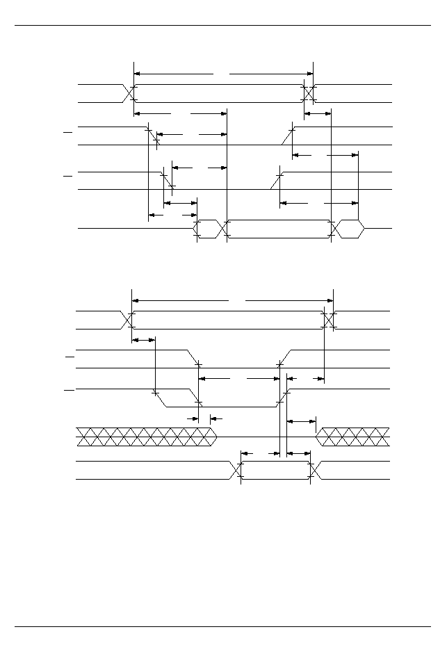
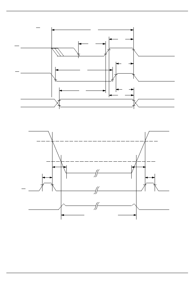
MEMORY READ CYCLE (NOTE 1)
œœœœœœ
œœœœœœ
ÃÃÃÃÃÃÃÃ
ÃÃÃÃÃÃÃÃ
œœœœœœœ
œœœœœœœ
ÃÃÃÃÃÃÃÃÃ
ÃÃÃÃÃÃÃÃÃ
ŒŒŒ
ŒŒŒ
ŒŒŒ
ŒŒŒ
t
RC
t
ACC
t
CO
t
OE
t
COE
t
COE
t
OH
t
OD
t
OD
OUTPUT
DATA VALID
V
IL
V
IH
V
IL
V
IH
V
IL
V
IH
V
IH
V
IL
V
IH
V
IH
V
IH
V
IL
V
OL
V
OH
V
OL
V
OH
ADDRESSES
CE
OE
D
OUT
MEMORY WRITE CYCLE 1 (NOTES 2, 6, AND 7)
œœœœœœœœœ
œœœœœœœœœ
ÃÃÃÃÃÃÃÃ
ÃÃÃÃÃÃÃÃ
t
WC
t
WR
V
IL
V
IH
V
IL
V
IH
V
IL
V
IH
V
IL
CE
œœœœ
œœœœ
V
IL
V
IL
V
IH
V
IL
V
IH
DATA IN
STABLE
t
WP
t
ODW
t
OEW
t
DH
t
DS
WE
ADDRESS
DQ0≠DQ7
t
AW
V
IH
V
IH
HIGH IMPEDANCE
DS1244Y
032697 9/12
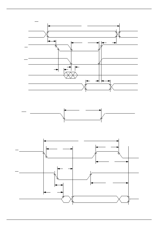
MEMORY WRITE CYCLE 2 (NOTES 2 AND 8)
œœœœœœœœœ
œœœœœœœœœ
ÃÃÃÃÃÃÃÃ
ÃÃÃÃÃÃÃÃ
t
WC
V
IL
V
IH
V
IL
V
IH
V
IL
V
IH
V
IL
CE
œœœœ
œœœœ
V
IL
V
IL
V
IH
V
IL
V
IH
DATA IN
STABLE
t
WP
t
COE
t
OEW
t
DH
t
DS
WE
ADDRESSES
DQ0≠DQ7
t
AW
V
IH
V
IH
t
WR
V
IL
V
IL
t
ODW
WE = V
IH
RESET FOR PHANTOM CLOCK
RST
t
RST
READ CYCLE TO PHANTOM CLOCK
ÃÃÃ
ÃÃÃ
ÃÃÃ
ÃÃÃ
OUTPUT DATA VALID
t
RC
t
CO
t
RR
t
OD
t
OE
t
ODO
t
COE
t
OEE
CE
OE
Q
DS1244Y
032697 10/12
WRITE CYCLE TO PHANTOM CLOCK
ÃÃÃÃÃÃÃ
ÃÃÃÃÃÃÃ
ÃÃÃÃÃÃ
ÃÃÃÃÃÃ
DATA IN STABLE
t
WC
t
WP
t
WR
t
CW
t
WR
t
DS
t
DH
t
DH
WE
CE
D
OE = V
IH
POWER≠DOWN/POWER≠UP CONDITION
DATA RETENTION TIME
t
DR
LEAKAGE CURRENT I
L
SUPPLIED FROM LITHIUM
CELL
t
R
t
REC
t
PD
t
F
V
CC
4.50V
3.2V
CE

DS1244Y
032697 11/12
NOTES:
1. WE is high for a read cycle.
2. OE = V
IH
or V
IL
. If OE = V
IH
during write cycle, the output buffers remain in a high impedance state.
3. t
WP
is specified as the logical AND of CE and WE. t
WP
is measured from the latter of CE or WE going low to the
earlier of CE or WE going high.
4. t
DH
, t
DS
are measured from the earlier of CE or WE going high.
5. These parameters are sampled with a 50 pF load and are not 100% tested.
6. If the CE low transition occurs simultaneously with or later than the WE low transition in Write Cycle 1, the output
buffers remain in a high impedance state during this period.
7. If the CE high transition occurs prior to or simultaneously with the WE high transition, the output buffers remain
in a high impedance state during this period.
8. If WE is low or the WE low transition occurs prior to or simultaneously with the CE low transition, the output buffers
remain in a high impedance state during this period.
9. The expected t
DR
is defined as accumulative time in the absence of V
CC
with the clock oscillator running.
10. t
WR
is a function of the latter occurring edge of WE or CE.
11. t
DH
and t
DS
are a function of the first occurring edge of WE or CE.
12. RST (Pin1) has an internal pull≠up resistor.
13. Real≠Time Clock Modules can be successfully processed through conventional wave≠soldering techniques as
long as temperature exposure to the lithium energy source contained within does not exceed +85
∞
C. Post solder
cleaning with water washing techniques is acceptable, provided that ultrasonic vibration is not used.
DS1244Y
032697 12/12
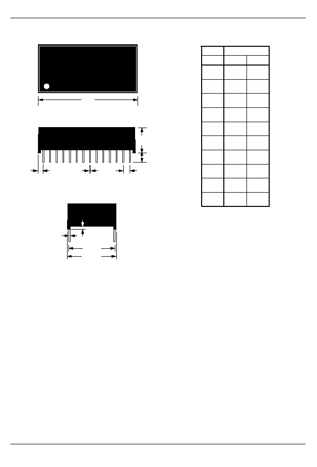
DS1244Y 256K NV SRAM WITH PHANTOM CLOCK
A
1
DIM
MIN
MAX
A
IN.
MM
B
IN.
MM
C IN.
MM
D IN.
MM
E
IN.
MM
F
IN.
MM
G IN.
MM
H IN.
MM
J
IN.
MM
K
IN.
MM
1.520
38.61
1.540
39.12
0.720
18.29
0.740
18.80
0.395
10.03
0.415
10.54
0.100
2.54
0.130
3.30
0.017
0.43
0.030
0.76
0.120
3.05
0.160
4.06
0.090
2.29
0.110
2.79
0.590
14.99
0.630
16.00
0.008
0.20
0.012
0.30
0.015
0.38
0.021
0.53
C
F
G
K
D
H
B
E
J
28≠PIN
PKG