 | –≠–ª–µ–∫—Ç—Ä–æ–Ω–Ω—ã–π –∫–æ–º–ø–æ–Ω–µ–Ω—Ç: DS1250Y | –°–∫–∞—á–∞—Ç—å:  PDF PDF  ZIP ZIP |
1 of 11
111999
FEATURES
10 years minimum data retention in the
absence of external power
Data is automatically protected during power
loss
Replaces 512k x 8 volatile static RAM,
EEPROM or Flash memory
Unlimited write cycles
Low-power CMOS
Read and write access times as fast as 70 ns
Lithium energy source is electrically
disconnected to retain freshness until power is
applied for the first time
Full
±
10% V
CC
operating range (DS1250Y)
Optional
±
5% V
CC
operating range
(DS1250AB)
Optional industrial temperature range of
-40
∞
C to +85
∞
C, designated IND
JEDEC standard 32-pin DIP package
New PowerCap Module (PCM) package
-
Directly surface-mountable module
-
Replaceable snap-on PowerCap provides
lithium backup battery
-
Standardized pinout for all nonvolatile
SRAM products
-
Detachment feature on PCM allows easy
removal using a regular screwdriver
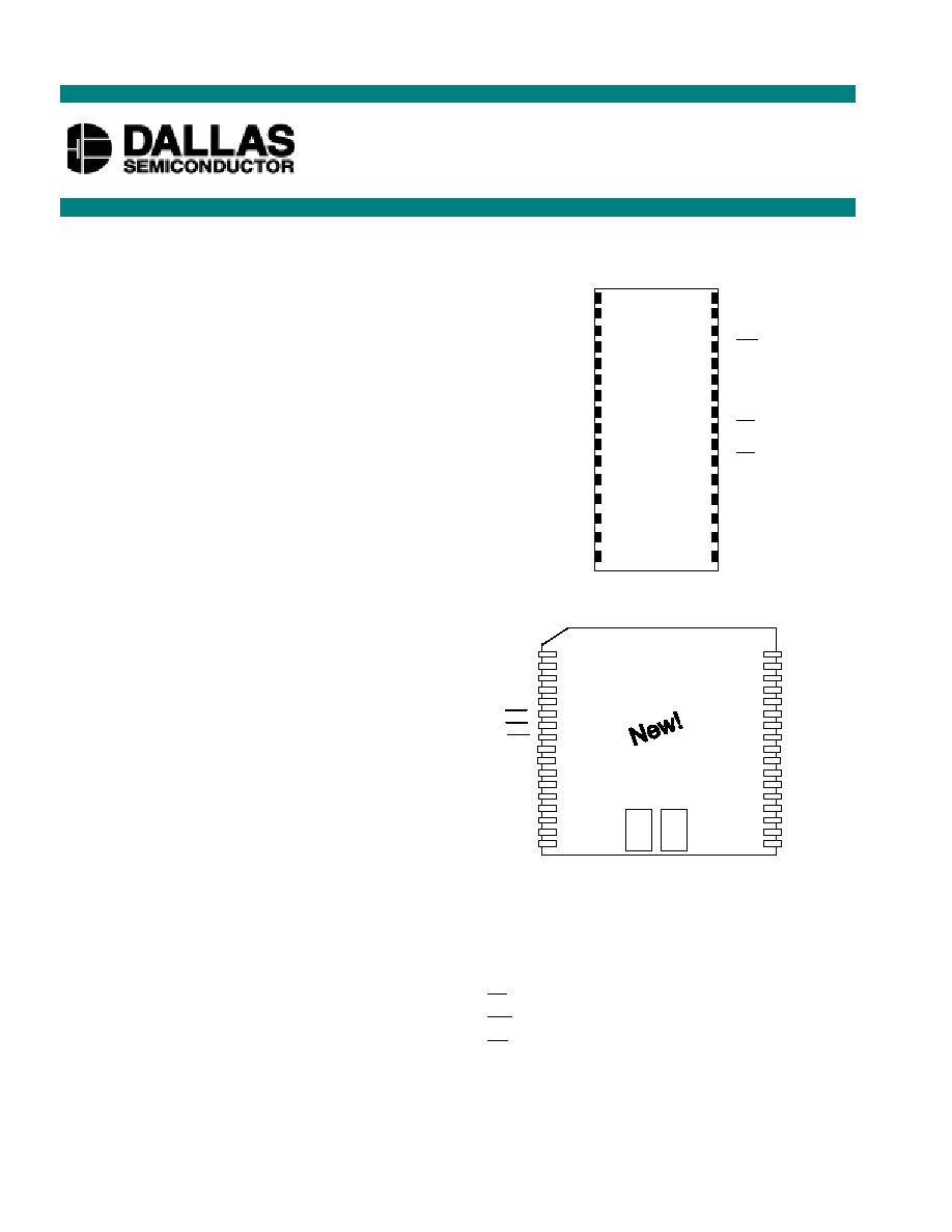
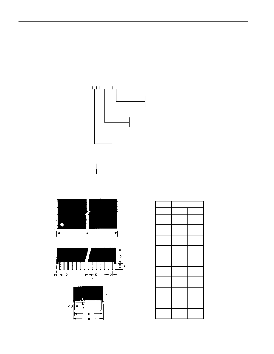
PIN ASSIGNMENT
PIN DESCRIPTION
A0 - A18
- Address Inputs
DQ0 - DQ7
- Data In/Data Out
CE
- Chip Enable
WE
- Write Enable
OE
- Output Enable
V
CC
- Power (+5V)
GND -
Ground
NC
- No Connect
DS1250Y/AB
4096k Nonvolatile SRAM
www.dalsemi.com
13
1
2
3
4
5
6
7
8
9
10
11
12
14
31
32-Pin ENCAPSULATED PACKAGE
740-mil EXTENDED
A14
A7
A5
A4
A3
A2
A1
A0
DQ1
DQ0
V
CC
A15
A17
WE
A13
A8
A9
A11
OE
A10
CE
DQ7
DQ5
DQ6
32
30
29
28
27
26
25
24
23
22
21
19
20
A16
A12
A6
A18
DQ2
GND
15
16
18
17
DQ4
DQ3
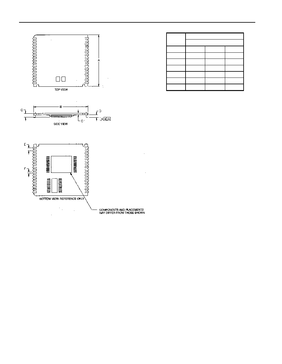
1
NC
2
3
A15
A16
NC
V
CC
WE
OE
CE
DQ7
DQ6
DQ5
DQ4
DQ3
DQ2
DQ1
DQ0
GND
4
5
6
7
8
9
10
11
12
13
14
15
16
17
A17
A14
33
32
31
30
29
28
27
26
25
24
23
22
21
20
19
18
A13
A12
A11
A10
A9
A8
A7
A6
A5
A4
A3
A2
A1
A0
34
A18
GND V
BAT
34-Pin POWERCAP MODULE (PCM)
(USES DS9034PC POWERCAP)

DS1250Y/AB
2 of 11
DESCRIPTION
The DS1250 4096k Nonvolatile SRAMs are 4,194,304-bit, fully static, nonvolatile SRAMs organized as
524,288 words by 8 bits. Each complete NV SRAM has a self-contained lithium energy source and
control circuitry which constantly monitors V
CC
for an out-of-tolerance condition. When such a condition
occurs, the lithium energy source is automatically switched on and write protection is unconditionally
enabled to prevent data corruption. DIP-package DS1250 devices can be used in place of existing 512k x
8 static RAMs directly conforming to the popular byte-wide 32-pin DIP standard. DS1250 devices in the
PowerCap Module package are directly surface mountable and are normally paired with a DS9034PC
PowerCap to form a complete Nonvolatile SRAM module. There is no limit on the number of write
cycles that can be executed and no additional support circuitry is required for microprocessor interfacing.
READ MODE
The DS1250 executes a read cycle whenever
WE
(Write Enable) is inactive (high) and
CE
(Chip Enable)
and
OE
(Output Enable) are active (low). The unique address specified by the 19 address inputs (A
0
-
A
18
) defines which of the 524,288 bytes of data is to be accessed. Valid data will be available to the eight
data output drivers within t
ACC
(Access Time) after the last address input signal is stable, providing that
CE
and
OE
(Output Enable) access times are also satisfied. If
OE
and
CE
access times are not satisfied,
then data access must be measured from the later-occurring signal (
CE
or
OE
) and the limiting parameter
is either t
CO
for
CE
or t
OE
for
OE
rather than address access.
WRITE MODE
The DS1250 executes a write cycle whenever the
WE
and
CE
signals are active (low) after address
inputs are stable. The later-occurring falling edge of
CE
or WE will determine the start of the write cycle.
The write cycle is terminated by the earlier rising edge of
CE
or
WE
. All address inputs must be kept
valid throughout the write cycle.
WE
must return to the high state for a minimum recovery time (t
WR
)
before another cycle can be initiated. The
OE
control signal should be kept inactive (high) during write
cycles to avoid bus contention. However, if the output drivers are enabled (
CE
and
OE
active) then
WE
will disable the outputs in t
ODW
from its falling edge.
DATA RETENTION MODE
The DS1250AB provides full functional capability for V
CC
greater than 4.75 volts and write protects by
4.5 volts. The DS1250Y provides full functional capability for V
CC
greater than 4.5 volts and write
protects by 4.25 volts. Data is maintained in the absence of V
CC
without any additional support circuitry.
The nonvolatile static RAMs constantly monitor V
CC
. Should the supply voltage decay, the NV SRAMs
automatically write protect themselves, all inputs become "don't care," and all outputs become high-
impedance. As V
CC
falls below approximately 3.0 volts, a power switching circuit connects the lithium
energy source to RAM to retain data. During power-up, when V
CC
rises above approximately 3.0 volts,
the power switching circuit connects external V
CC
to RAM and disconnects the lithium energy source.
Normal RAM operation can resume after V
CC
exceeds 4.75 volts for the DS1250AB and 4.5 volts for the
DS1250Y.
FRESHNESS SEAL
Each DS1250 device is shipped from Dallas Semiconductor with its lithium energy source disconnected,
guaranteeing full energy capacity. When V
CC
is first applied at a level greater than 4.25 volts, the lithium
energy source is enabled for battery back-up operation.
DS1250Y/AB
3 of 11
PACKAGES
The DS1250 is available in two packages: 32-pin DIP and 34-pin PowerCap Module (PCM). The 32-pin
DIP integrates a lithium battery, an SRAM memory and a nonvolatile control function into a single
package with a JEDEC-standard 600-mil DIP pinout. The 34-pin PowerCap Module integrates SRAM
memory and nonvolatile control into a module base along with contacts for connection to the lithium
battery in the DS9034PC PowerCap. The PowerCap Module package design allows a DS1250 PCM
device to be surface mounted without subjecting its lithium backup battery to destructive high-
temperature reflow soldering. After a DS1250 PCM module base is reflow soldered, a DS9034PC
PowerCap is snapped on top of the PCM to form a complete Nonvolatile SRAM module. The DS9034PC
is keyed to prevent improper attachment. DS1250 module bases and DS9034PC PowerCaps are ordered
separately and shipped in separate containers. See the DS9034PC data sheet for further information.
ABSOLUTE MAXIMUM RATINGS*
Voltage on Any Pin Relative to Ground
-0.3V to +7.0V
Operating Temperature
0∞C to 70∞C, -40∞C to +85∞C for IND parts
Storage Temperature
-40∞C to +70∞C, -40∞C to +85∞C for IND parts
Soldering Temperature
260∞C for 10 seconds
*
This is a stress rating only and functional operation of the device at these or any other conditions
above those indicated in the operation sections of this specification is not implied. Exposure to
absolute maximum rating conditions for extended periods of time may affect reliability.
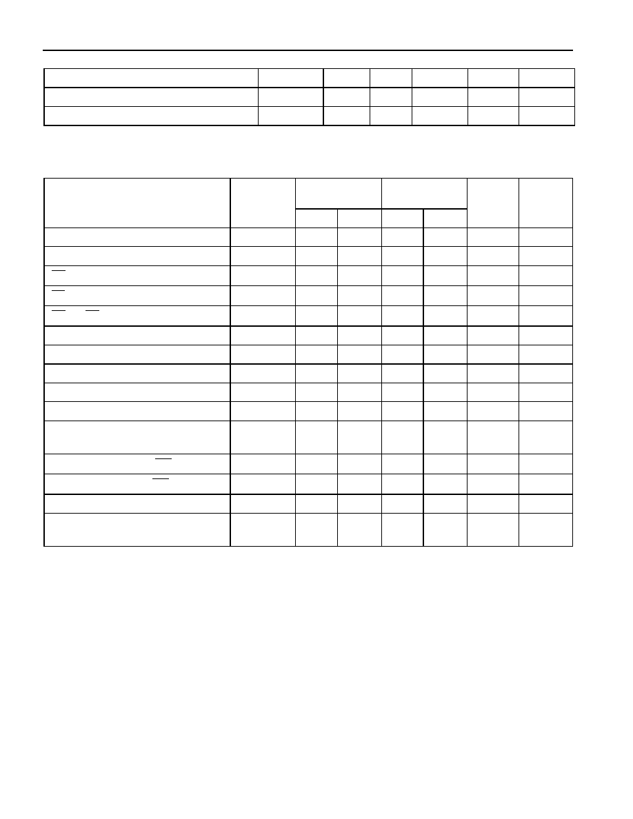
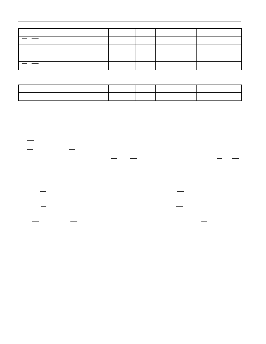
RECOMMENDED DC OPERATING CONDITIONS (t
A
: See Note 10)
PARAMETER
SYMBOL
MIN
TYP
MAX
UNITS NOTES
DS1250AB Power Supply Voltage
V
CC
4.75
5.0
5.25
V
DS1250Y Power Supply Voltage
V
CC
4.5
5.0
5.5
V
Logic 1
V
IH
2.2
V
CC
V
Logic 0
V
IL
0.0
+0.8
V
DC ELECTRICAL (V
CC
=5V
±
=
5% for DS1250AB)
CHARACTERISTICS (t
A
: See Note 10) (V
CC
=5V
±
=
10% for DS1250Y)
PARAMETER
SYMBOL
MIN
TYP
MAX
UNITS NOTES
Input Leakage Current
I
IL
-1.0
+1.0
µ
A
I/O Leakage Current
CE
V
IH
V
CC
I
IO
-1.0
+1.0
µ
A
Output Current @ 2.2V
I
OH
-1.0
mA
Output Current @ 0.4V
I
OL
2.0
mA
Standby Current
CE
=2.2V
I
CCS1
5.0
10.0
mA
Standby Current
CE
=V
CC
-0.5V
I
CCS2
3.0
5.0
mA
Operating Current
I
CCO1
85
mA
Write Protection Voltage (DS1250AB)
V
TP
4.50
4.62
4.75
V
Write Protection Voltage (DS1250Y)
V
TP
4.25
4.37
4.5
V
DS1250Y/AB
4 of 11
CAPACITANCE (t
A
=25
∞
C)
PARAMETER
SYMBOL
MIN
TYP
MAX
UNITS NOTES
Input Capacitance
C
IN
5
10
pF
Input/Output Capacitance
C
I/O
5
10
pF
AC ELECTRICAL (V
CC
=5V
±
=
5% for DS1250AB)
CHARACTERISTICS (t
A
: See Note 10) (V
CC
=5V
±
=
10% for DS1250Y)
DS1250AB-70
DS1250Y-70
DS1250AB-100
DS1250Y-100
PARAMETER
SYMBOL
MIN
MAX
MIN
MAX
UNITS NOTES
Read Cycle Time
t
RC
70
100
ns
Access Time
t
ACC
70
100
ns
OE
to Output Valid
t
OE
35
50
ns
CE
to Output Valid
t
CO
70
100
ns
OE
or
CE
to Output Active
t
COE
5
5
ns
5
Output High Z from Deselection
t
OD
25
35
ns
5
Output Hold from Address Change
t
OH
5
5
ns
Write Cycle Time
t
WC
70
100
ns
Write Pulse Width
t
WP
55
75
ns
3
Address Setup Time
t
AW
0
0
ns
Write Recovery Time
t
WR1
t
WR2
5
15
5
15
ns
ns
12
13
Output High Z from
WE
t
ODW
25
35
ns
5
Output Active from
WE
t
OEW
5
5
ns
5
Data Setup Time
t
DS
30
40
ns
4
Data Hold Time
t
DH1
t
DH2
0
10
0
10
ns
ns
12
13
DS1250Y/AB
5 of 11
READ CYCLE
SEE NOTE 1
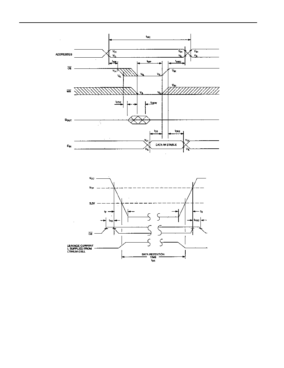
WRITE CYCLE 1
SEE NOTES 2, 3, 4, 6, 7, 8, and 12
DS1250Y/AB
6 of 11
WRITE CYCLE 2
SEE NOTES 2, 3, 4, 6, 7, 8, and 13
POWER-DOWN/POWER-UP CONDITION
SEE NOTE 11
DS1250Y/AB
7 of 11
POWER-DOWN/POWER-UP TIMING (t
A
: See Note 10)
PARAMETER
SYMBOL
MIN
TYP
MAX
UNITS NOTES
CE
,
WE
at V
IH
before Power-Down
t
PD
0
µ
s
11
V
CC
slew from V
TP
to 0V
t
F
300
µ
s
V
CC
slew from 0V to V
TP
t
R
300
µ
s
CE
,
WE
at V
IH
after Power-Up
t
REC
2
125
ms
(t
A
=25
∞
C)
PARAMETER
SYMBOL
MIN
TYP
MAX
UNITS NOTES
Expected Data Retention Time
t
DR
10
years
9
WARNING:
Under no circumstance are negative undershoots, of any amplitude, allowed when device is in battery
backup mode.
NOTES:
1.
WE
is high for a Read Cycle.
2.
OE
= V
IH
or V
IL
. If
OE
= V
IH
during write cycle, the output buffers remain in a high-impedance state.
3.
t
WP
is specified as the logical AND of
CE
and
WE
. t
WP
is measured from the latter of
CE
or
WE
going low to the earlier of
CE
or
WE
going high.
4.
t
DH
, t
DS
are measured from the earlier of
CE
or
WE
going high.
5.
These parameters are sampled with a 5 pF load and are not 100% tested.
6.
If the
CE
low transition occurs simultaneously with or latter than the
WE
low transition, the output
buffers remain in a high-impedance state during this period.
7.
If the
CE
high transition occurs prior to or simultaneously with the
WE
high transition, the output
buffers remain in high-impedance state during this period.
8.
If
WE
is low or the
WE
low transition occurs prior to or simultaneously with the
CE
low transition,
the output buffers remain in a high-impedance state during this period.
9.
Each DS1250 has a built-in switch that disconnects the lithium source until V
CC
is first applied by the
user. The expected t
DR
is defined as accumulative time in the absence of V
CC
starting from the time
power is first applied by the user.
10.
All AC and DC electrical characteristics are valid over the full operating temperature range. For
commercial products, this range is 0
∞
C to 70
∞
C. For industrial products (IND), this range is -40
∞
C to
+85
∞
C.
11.
In a power-down condition the voltage on any pin may not exceed the voltage on V
CC
.
12.
t
WR1
and t
DH1
are measured from
WE
going high.
13.
t
WR2
and t
DH2
are measured from
CE
going high.
14.
DS1250 DIP modules are recognized by Underwriters Laboratory (U.L.
) under file E99151.
DS1250 PowerCap modules are pending U.L. review. Contact the factory for status.
DS1250Y/AB
8 of 11
DC TEST CONDITIONS
AC TEST CONDITIONS
Outputs Open
Output Load: 100 pF + 1TTL Gate
Cycle = 200 ns for operating current
Input Pulse Levels: 0 - 3.0V
All voltages are referenced to ground
Timing Measurement Reference Levels
Input: 1.5V
Output: 1.5V
Input pulse Rise and Fall Times: 5 ns
ORDERING INFORMATION
DS1250 TTP - SSS - III
Operating Temperature Range
blank: 0
∞
to 70
∞
IND: -40
∞
to +85
∞
C
Access Speed
70:
70 ns
100:
100 ns
Package Type
blank: 32-pin 600 mil DIP
P:
34-pin PowerCap Module
Device Type
AB:
±
5%
Y:
±
10%
DS1250Y/AB NONVOLATILE SRAM, 32-PIN, 740 MIL-EXTENDED DIP
MODULE
PKG
32-PIN
DIM
MIN
MAX
A IN.
MM
1.680
42.67
1.700
43.18
B IN.
MM
0.720
18.29
0.740
18.80
C IN.
MM
0.355
9.02
0.375
9.52
D IN.
MM
0.080
2.03
0.110
2.79
E IN.
MM
0.015
0.38
0.025
0.63
F IN.
MM
0.120
3.05
0.160
4.06
G IN.
MM
0.090
2.29
0.110
2.79
H IN.
MM
0.590
14.99
0.630
16.00
J IN.
MM
0.008
0.20
0.012
0.30
K IN.
MM
0.015
0.38
0.021
0.53
DS1250Y/AB
9 of 11
DS1250Y/AB NONVOLATILE SRAM, 34-PIN POWERCAP MODULE
INCHES
PKG
DIM
MIN
NOM
MAX
A
0.920
0.925
0.930
B
0.980
0.985
0.990
C
-
-
0.080
D
0.052
0.055
0.058
E
0.048
0.050
0.052
F
0.015
0.020
0.025
G
0.020
0.025
0.030
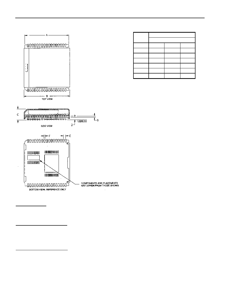
DS1250Y/AB
10 of 11
DS1250Y/AB NONVOLATILE SRAM, 34-PIN POWERCAP MODULE WITH
POWERCAP
INCHES
PKG
DIM
MIN
NOM
MAX
A
0.920
0.925
0.930
B
0.955
0.960
0.965
C
0.240
0.245
0.250
D
0.052
0.055
0.058
E
0.048
0.050
0.052
F
0.015
0.020
0.025
G
0.020
0.025
0.030
ASSEMBLY AND USE
Reflow soldering
Dallas Semiconductor recommends that PowerCap Module bases experience one pass through solder
reflow oriented label-side up (live-bug).
Hand soldering and touch-up
Do not touch soldering iron to leads for more than 3 seconds. To solder, apply flux to the pad, heat the
lead frame pad and apply solder. To remove part, apply flux, heat pad until solder reflows, and use a
solder wick.
LPM replacement in a socket
To replace a Low Profile Module in a 68-pin PLCC socket, attach a DS9034PC PowerCap to a module
base then insert the complete module into the socket one row of leads at a time, pushing only on the
corners of the cap. Never apply force to the center of the device. To remove from a socket, use a PLCC
extraction tool and ensure that it does not hit or damage any of the module IC components. Do not use
any other tool for extraction.
DS1250Y/AB
11 of 11
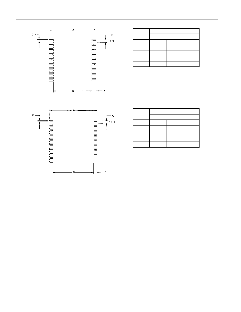
RECOMMENDED POWERCAP MODULE LAND PATTERN
INCHES
PKG
DIM
MIN
NOM
MAX
A
-
1.050
-
B
-
0.826
-
C
-
0.050
-
D
-
0.030
-
E
-
0.112
-
RECOMMENDED POWERCAP MODULE SOLDER STENCIL
INCHES
PKG
DIM
MIN
NOM
MAX
A
-
1.050
-
B
-
0.890
-
C
-
0.050
-
D
-
0.030
-
E
-
0.080
-