 | –≠–ª–µ–∫—Ç—Ä–æ–Ω–Ω—ã–π –∫–æ–º–ø–æ–Ω–µ–Ω—Ç: DS1308 | –°–∫–∞—á–∞—Ç—å:  PDF PDF  ZIP ZIP |

1 of 14
070900
FEATURES
Real time clock counts seconds, minutes,
hours, date of the month, month, day of the
week, and year with leap year compensation
valid up to 2100
56 byte nonvolatile RAM for data storage
2-wire serial interface
Programmable squarewave output signal
Automatic power-fail detect and switch
circuitry
Consumes less than 500 nA in battery backup
mode with oscillator running
Optional industrial temperature range
-40∞C to +85∞C (IND) available for DS1307
and DS1308
DS1307 available in 8-pin DIP or SOIC
DS1308 available in 36-pin SMD BGA (Ball
Grid Array)
DS1308 accuracy is better than ±2
minute/month at 25∞C
Recognized by Underwriters Laboratory
ORDERING INFORMATION
DS1307 8-Pin
DIP
DS1307Z
8-Pin SOIC (150 mil)
DS1307N
8-Pin DIP (Industrial)
DS1307ZN
8-Pin SOIC (Industrial)
DS1308 36-Pin
BGA
DS1308N
36-Pin BGA (Industrial)
PIN ASSIGNMENT
PIN DESCRIPTION DS1307/DS1308
V
CC
- Primary Power Supply
X1, X2
- 32.768 kHz Crystal Connection
V
BAT
-
+3V
Battery
Input
GND -
Ground
SDA
- Serial Data
SCL
- Serial Clock
SQW/OUT
- Square wave/Output Driver
DS1308 PIN IDENTIFIER
V
CC
- C2, C3, D2, D3
V
BAT
- A4, A5, B4, B5
SDA
- C7, C8, D7, D8
SCL
- A7, A8, B7, B8
SQW/OUT
- C4, C5, D4, D5
GND
- All Remaining Balls
DS1307/DS1308
64 X 8 Serial Real Time Clock
www.dalsemi.com
DS1307Z 8-Pin SOIC (150 mil)
DS1307 8-Pin DIP (300 mil)
X1
X2
V
BAT
GND
V
CC
SQW/OUT
SCL
l
2
3
4
8
7
6
5
SDA
A B
D
C
DS1308 36-Pin SMD BGA
(Top View)
1
2
3
4
5
6
7
8
9
GND
VBAT
GND
SCL
GND
GND
SDA
GND
SQW/
OUT
VCC
GND
l
2
3
4
8
7
6
5
X1
X2
V
BAT
GND
V
CC
SQW/OUT
SCL
SDA
DS1307/1308
2 of 14
DESCRIPTION
The DS1307 Serial Real Time Clock is a low power, full BCD clock/calendar plus 56 bytes of
nonvolatile SRAM. Address and data are transferred serially via a 2-wire bi-directional bus. The
clock/calendar provides seconds, minutes, hours, day, date, month, and year information. The end of the
month date is automatically adjusted for months with less than 31 days, including corrections for leap
year. The clock operates in either the 24-hour or 12-hour format with AM/PM indicator. The DS1307
has a built-in power sense circuit which detects power failures and automatically switches to the battery
supply.
The DS1308 incorporates the DS1307 chip with a 32.768 kHz crystal in a surface mountable, 36-pin ball
grid array package (BGA). The close proximity of the embedded crystal to the high impedance crystal
input pins on the DS1307 minimizes capacitive loading and noise injection problems associated with
many other oscillator designs. The total area required for installation is less than that of one United States
dime: thus, minimizing PCB space required.
OPERATION
The DS1307/1308 operates as a slave device on the serial bus. Access is obtained by implementing a
START condition and providing a device identification code followed by a register address. Subsequent
registers can be accessed sequentially until a STOP condition is executed. When V
CC
falls below 1.25 x
V
BAT
the device terminates an access in progress and resets the device address counter. Inputs to the
device will not be recognized at this time to prevent erroneous data from being written to the device from
an out of tolerance system. When V
CC
falls below V
BAT
the device switches into a low current battery
backup mode. Upon power up, the device switches from battery to V
CC
when V
CC
is greater than V
BAT
+0.2V and recognizes inputs when V
CC
is greater than 1.25 x V
BAT
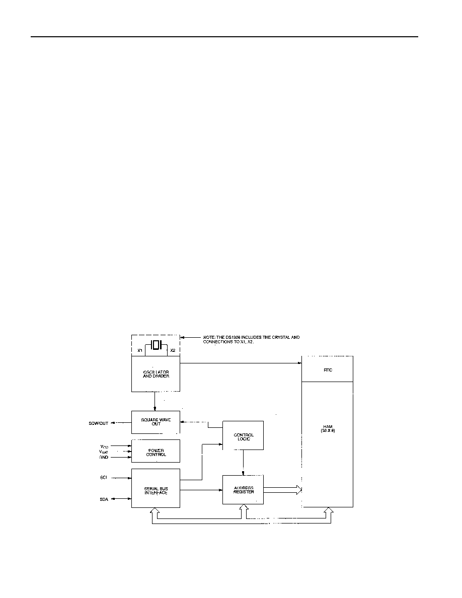
. The block diagram in Figure 1 shows
the main elements of the Serial Real Time Clock.
DS1307/DS1308 BLOCK DIAGRAM Figure 1

DS1307/1308
3 of 14
SIGNAL DESCRIPTIONS
V
CC
, GND - DC power is provided to the device on these pins. V
CC
is the +5 volt input. When 5 volts is
applied within normal limits, the device is fully accessible and data can be written and read. When a
3-volt battery is connected to the device and V
CC
is below 1.25 x V
BAT
, reads and writes are inhibited.
However, the Timekeeping function continues unaffected by the lower input voltage. As V
CC
falls below
V
BAT
the RAM and timekeeper are switched over to the external power supply (nominal 3.0V DC) at
V
BAT
.
V
BAT
- Battery input for any standard 3-volt lithium cell or other energy source. Battery voltage must be
held between 2.0 and 3.5 volts for proper operation. The nominal write protect trip point voltage at which
access to the real time clock and user RAM is denied is set by the internal circuitry as 1.25 x V
BAT
nominal. A lithium battery with 48 mAhr or greater will back up the DS1307/DS1308 for more than 10
years in the absence of power at 25 degrees C.
SCL (Serial Clock Input) - SCL is used to synchronize data movement on the serial interface.
SDA (Serial Data Input/Output) - SDA is the input/output pin for the 2-wire serial interface. The SDA
pin is open drain which requires an external pullup resistor.
SQW/OUT (Square Wave/ Output Driver) - When enabled, the SQWE bit set to 1, the SQW/OUT pin
outputs one of four square wave frequencies (1 Hz, 4 kHz, 8 kHz, 32 kHz). The SQW/OUT pin is open
drain which requires an external pullup resistor. SQW/OUT will operate with either Vcc or Vbat applied.
NOTE: X1, X2 are not applicable for the DS1308 or DS1308N.
X1, X2 - Connections for a standard 32.768 kHz quartz crystal. The internal oscillator circuitry is
designed for operation with a crystal having a specified load capacitance (CL) of 12.5 pF.
For more information on crystal selection and crystal layout considerations, please consult Application
Note 58, "Crystal Considerations with Dallas Real Time Clocks." The DS1307 can also be driven by an
external 32.768 kHz oscillator. In this configuration, the X1 pin is connected to the external oscillator
signal and the X2 pin is floated.
Please review Application Note 95, "Interfacing the DS1307/DS1308 with a 8051-Compatible
Microcontroller" for additional information.
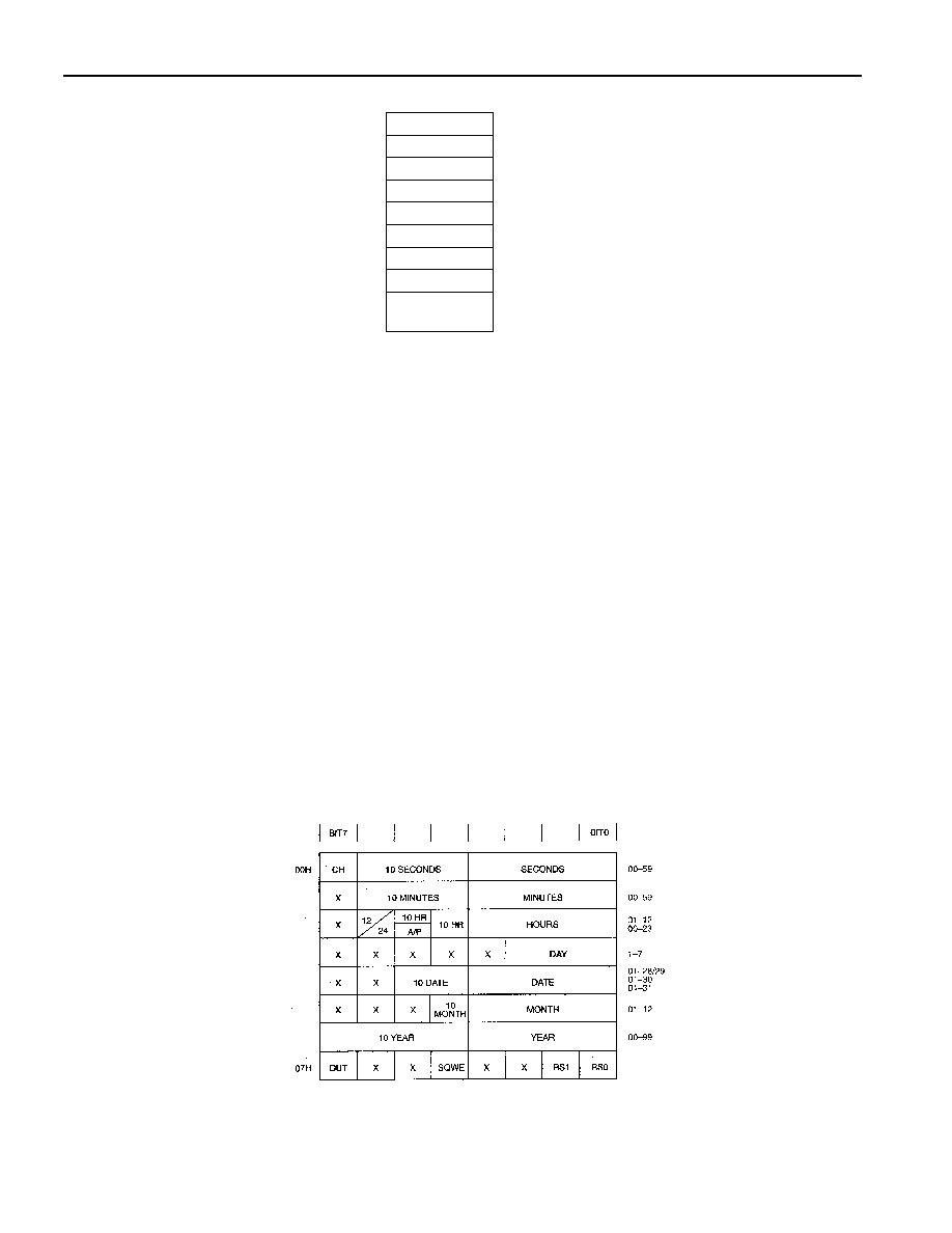
RTC AND RAM ADDRESS MAP
The address map for the RTC and RAM registers of the DS1307/DS1308 is shown in Figure 2. The real
time clock registers are located in address locations 00h to 07h. The RAM registers are located in address
locations 08h to 3Fh. During a multi-byte access, when the address pointer reaches 3Fh, the end of RAM
space, it wraps around to location 00h, the beginning of the clock space.
DS1307/1308
4 of 14
DS1307 ADDRESS MAP Figure 2
CLOCK AND CALENDAR
The time and calendar information is obtained by reading the appropriate register bytes. The real time
clock registers are illustrated in Figure 3. The time and calendar are set or initialized by writing the
appropriate register bytes. The contents of the time and calendar registers are in the Binary-Coded
Decimal (BCD) format. Bit 7 of Register 0 is the Clock Halt (CH) bit. When this bit is set to a 1, the
oscillator is disabled. When cleared to a 0, the oscillator is enabled.
Please note that the initial power on state of all registers is not defined. Therefore it is important to
enable the oscillator (CH bit=0) during initial configuration.
The DS1307/DS1308 can be run in either 12-hour or 24-hour mode. Bit 6 of the hours register is defined
as the 12- or 24-hour mode select bit. When high, the 12-hour mode is selected. In the 12-hour mode, bit
5 is the AM/PM bit with logic high being PM. In the 24-hour mode, bit 5 is the second 10 hour bit (20-23
hours).
On a 2-wire START, the current time is transferred to a second set of registers. The time information is
read from these secondary registers, while the clock may continue to run. This eliminates the need to re-
read the registers in case of an update of the main registers during a read.
DS1307/DS1308 TIMEKEEPER REGISTERS Figure 3
SECONDS
MINUTES
HOURS
DAY
DATE
MONTH
YEAR
CONTROL
RAM
56 x 8
00H
07H
08H
3FH
DS1307/1308
5 of 14
CONTROL REGISTER
The DS1307/DS1308 Control Register is used to control the operation of the SQW/OUT pin.
BIT 7
BIT 6
BIT 5
BIT 4
BIT 3
BIT 2
BIT 1
BIT 0
OUT
X
X
SQWE
X
X
RS1
RS0
OUT (Output control): This bit controls the output level of the SQW/OUT pin when the square wave
output is disabled. If SQWE=0, the logic level on the SQW/OUT pin is 1 if OUT=1 and is 0 if OUT=0.
SQWE (Square Wave Enable): This bit, when set to a logic 1, will enable the oscillator output. The
frequency of the square wave output depends upon the value of the RS0 and RS1 bits.
RS (Rate Select): These bits control the frequency of the square wave output when the square wave
output has been enabled. Table 1 lists the square wave frequencies that can be selected with the RS bits.
SQUAREWAVE OUTPUT FREQUENCY Table 1
RS1
RS0
SQW OUTPUT
FREQUENCY
0
0
1 Hz
0
1
4.096 kHz
1
0
8.192 kHz
1
1
32.768 kHz
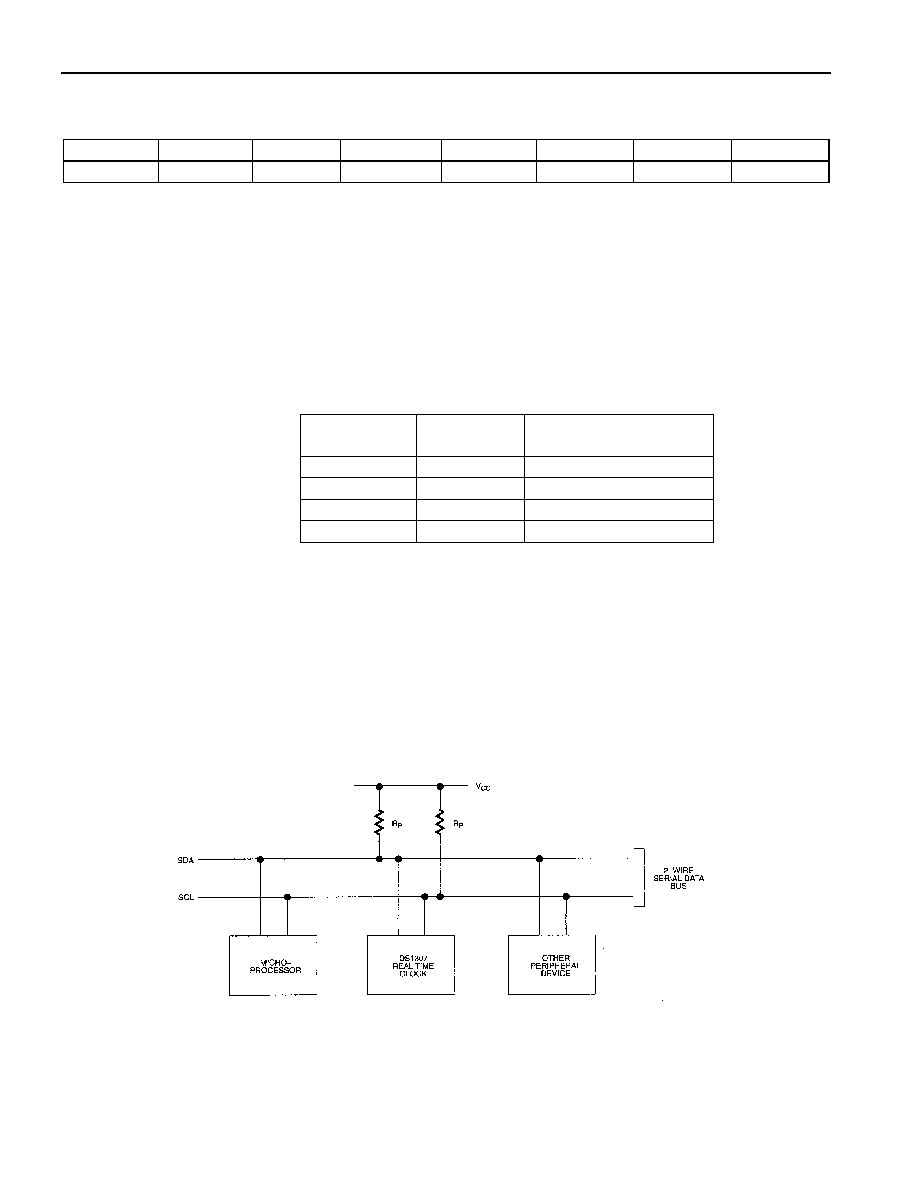
2-WIRE SERIAL DATA BUS
The DS1307 supports a bi-directional 2-wire bus and data transmission protocol. A device that sends
data onto the bus is defined as a transmitter and a device receiving data as a receiver. The device that
controls the message is called a master. The devices that are controlled by the master are referred to as
slaves. The bus must be controlled by a master device which generates the serial clock (SCL), controls
the bus access, and generates the START and STOP conditions. The DS1307/DS1308 operates as a slave
on the 2-wire bus. A typical bus configuration using this 2-wire protocol is show in Figure 4.
TYPICAL 2-WIRE BUS CONFIGURATION Figure 4