 | –≠–ª–µ–∫—Ç—Ä–æ–Ω–Ω—ã–π –∫–æ–º–ø–æ–Ω–µ–Ω—Ç: DS1501YN | –°–∫–∞—á–∞—Ç—å:  PDF PDF  ZIP ZIP |
1 of 20
REV: 031704
Note: Some revisions of this device may incorporate deviations from published specifications known as errata. Multiple revisions of any device
may be simultaneously available through various sales channels. For information about device errata, click here:
www.maxim-ic.com/errata
.
GENERAL DESCRIPTION
The DS1501/DS1511 are full-function, year 2000-
compliant real-time clock/calendars (RTCs) with an
RTC alarm, watchdog timer, power-on reset, battery
monitors, 256 bytes NV SRAM, and a 32.768kHz
output. User access to all registers within the
DS1501/DS1511 is accomplished with a byte-wide
interface, as shown in Figure 8. The RTC registers
contain century, year, month, date, day, hours,
minutes, and seconds data in 24-hour binary-coded
decimal (BCD) format. Corrections for day of month
and leap year are made automatically.
APPLICATIONS
Remote Systems
Battery-Backed Systems
Telecom Switches
Office Equipment
Consumer Electronics
ORDERING INFORMATION
PART TEMP
RANGE
PIN-PACKAGE
DS1501YN
-40∞C to +85∞C
28 DIP (600 mil)
DS1501YEN
-40∞C to +85∞C
28 TSOP
DS1501YSN
-40∞C to +85∞C
28 SO (330 mil)
DS1501WN
-40∞C to +85∞C
28 DIP (600 mil)
DS1501WEN
-40∞C to +85∞C
28 TSOP
DS1501WSN
-40∞C to +85∞C
28 SO (330 mil)
DS1511Y
0∞C to +70∞C
28 Module (720 mil)
DS1511W
0∞C to +70∞C
28 Module (720 mil)
Selector Guide appears at end of data sheet.
Typical Operating Circuits appears at end of data sheet.
FEATURES
ß BCD-Coded Century, Year, Month, Date, Day,
Hours, Minutes, and Seconds with Automatic
Leap-Year Compensation Valid Up to the Year
2100
ß Programmable Watchdog Timer and RTC Alarm
ß Century Register; Y2K-Compliant RTC
ß +3.3 or +5V Operation
ß Precision Power-On Reset
ß Power-Control Circuitry Support System Power-
On from Date/Day/Time Alarm or Key
Closure/Modem-Detect Signal
ß 256 Bytes Battery-Backed NV SRAM
ß Auxiliary Battery Input
ß Accuracy of DS1511 Better than ±1
Minute/Month at +25∞C
ß Day-of-Week/Date Alarm Register
ß Crystal Select Bit Allow RTC to Operate with 6pF
or 12.6pF Crystal
ß Battery Voltage-Level Indicator Flags
ß Available as Chip (DS1501) or Stand-Alone
Module with Embedded Battery and Crystal
(DS1511)
ß UL Recognized
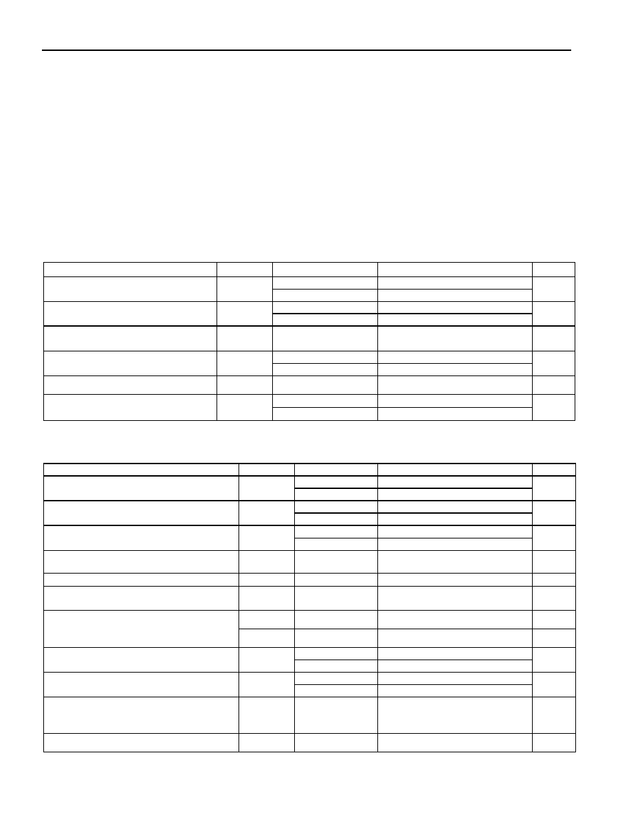
PIN CONFIGURATION
DS1501/DS1511
Y2K-Compliant Watchdog
Real-Time Clocks
www.maxim-ic.com
TOP VIEW
Dallas
Semiconductor
DS1501
1
2
3
4
5
6
7
8
9
10
11
12
13
14
28
27
26
25
24
23
22
21
20
19
18
17
16
15
SQW
GND
DQ7
DQ6
DQ5
DQ4
DQ3
WE
KS
OE
CE
V
CC
V
BAUX
V
BAT
X1
X2
A4
A3
A2
A1
A0
DQ0
DQ1
DQ2
GND
PWR
RST
IRQ
DIP, SO
Pin Configurations are continued at end of data sheet.
DS1501/DS1511 Y2KC Watchdog Real-Time Clocks
2 of 20
ABSOLUTE MAXIMUM RATINGS
Voltage Range on Any Pin Relative to Ground........................................................................-0.5V to +6.0V
Operating Temperature Range (Module).................................................................................0∞C to +70∞C
Operating Temperature Range, DS1501
........................................................
-40∞C to +85∞C (Note 1)
Operating Temperature Range, DS1511.................................................................................0∞C to +70∞C
Storage Temperature Range, DS1501
...................................................................
-55∞C to +125∞C
Storage Temperature Range, DS1511.................................................................................-40∞C to +70∞C
Soldering Temperature (DIP, Module)..........................+260∞C Lead Temperature for 10 seconds (max) (Note 2)
Soldering Temperature (SO, TSOP)
........................
See IPC/JEDEC J-STD-020A for Surface-Mount Devices
Stresses beyond those listed under "Absolute Maximum Ratings" may cause permanent damage to the device. These are stress ratings only,
and functional operation of the device at these or any other conditions beyond those indicated in the operational sections of the specifications is
not implied. Exposure to the absolute maximum rating conditions for extended periods may affect device reliability.
RECOMMENDED DC OPERATING CONDITIONS
(V
CC
= 3.3V or 5V ±10%, T
A
= 0∞C to +70∞C; V
CC
= 3.3V or 5V ±10%, T
A
= -40∞C to +85∞C.)
PARAMETER SYMBOL
CONDITIONS
MIN
TYP
MAX
UNITS
5V (Y)
4.5
5.0
5.5
Power Supply Voltage (Note 3)
V
CC
3.3V (W)
3.0
3.3
3.6
V
Y 2.2
V
CC
+ 0.3
Logic 1 Voltage All Inputs (Note 3)
V
IH
W 2.0
V
CC
+ 0.3
V
Pullup Voltage,
IRQ, PWR, and
RST Outputs (Note 3)
V
PU
5.5
V
Y -0.3
+0.8
Logic 0 Voltage All Inputs (Note 3)
V
IL
W -0.3
+0.6
V
Battery Voltage (Note 3)
V
BAT
2.5
3.0
3.7
V
Y 2.5
3.0
5.3
Auxiliary Battery Voltage (Note 3)
V
BAUX
W 2.5
3.0
3.7
V
DC ELECTRICAL CHARACTERISTICS
(V
CC
= 3.3V or 5V ±10%, T
A
= 0∞C to +70∞C; V
CC
= 3.3V or 5V ±10%, T
A
= -40∞C to +85∞C.)
PARAMETER SYMBOL
CONDITIONS
MIN
TYP
MAX
UNITS
Y
15
Active Supply Current (Note 4)
I
CC
W
10
mA
Y
5
TTL Standby Current (
CE = V
IH
)
I
CC1
W
4
mA
Y
5
CMOS Standby Current
(
CE = V
CC
- 0.2V)
I
CC2
W
4
mA
Input Leakage Current (Any Input)
I
IL
-1
+1 mA
Output Leakage Current (Any Output)
I
OL
-1
+1 mA
Output Logic 1 Voltage
(I
OUT
= -1.0mA)
V
OH
(Note
3)
2.4
V
V
OL1
(Note
3)
0.4
V
Output Logic 0 Voltage (I
OUT
= 2.1mA,
DQ0≠7; I
OUT
= 5.0mA,
IRQ, I
OUT
=
7.0mA,
PWR and RST)
V
OL2
(Notes
3,
5)
0.4
V
Y
2.0
Battery Low, Flag Trip Point (Note 2)
V
BLF
W
1.9
V
Y 4.20
4.50
Power-Fail Voltage (Note 2)
V
PF
W 2.75
2.97
V
Battery Switchover Voltage (Notes 3, 6)
V
SO
V
BAT,
V
BAUX,
or V
PF
V
Battery Leakage Current
I
LKG
100 nA
DS1501/DS1511 Y2KC Watchdog Real-Time Clocks
3 of 20
DC ELECTRICAL CHARACTERISTICS
(V
CC
= 0V; T
A
= 0∞C to +70∞C; V
CC
= 0V, T
A
= -40∞C to +85∞C.)
PARAMETER SYMBOL
CONDITIONS
MIN
TYP
MAX
UNITS
Battery Current, BB32 = 0,
EOSC = 0
I
BAT1
(Note 7)
0.27
1.0 mA
Battery Current, BB32 = 0,
EOSC = 1
I
BAT2
(Note 7)
0.01
0.1 mA
V
BAUX
Current BB32 = 1, SQW Open
I
BAUX
(Note 7)
2 mA
CRYSTAL SPECIFICATIONS*
PARAMETER SYMBOL
CONDITIONS
MIN
TYP
MAX
UNITS
Nominal Frequency
f
O
32.768 kHz
Series Resistance
ESR
45
k
W
Load Capacitance
C
L
6 pF
*The crystal, traces, and crystal input pins should be isolated from RF generating signals. Refer to Application Note 58: Crystal Considerations
for Dallas Real-Time Clocks for additional specifications.
AC OPERATING CHARACTERISTICS
(V
CC
= 5V ±10%, T
A
= 0∞C to +70∞C; V
CC
= 5V ±10%, T
A
= -40∞C to +85∞C.)
PARAMETER SYMBOL
CONDITIONS
MIN
TYP
MAX
UNITS
Read Cycle Time
t
RC
70 ns
Address Access Time
t
AA
70 ns
CE to DQ Low-Z
t
CEL
(Note 8)
5 ns
CE Access Time
t
CEA
70 ns
CE Data-Off Time
t
CEZ
(Note 8)
25 ns
OE to DQ Low-Z (0∞C to +85∞C)
t
OEL
(Note 8)
5 ns
OE to DQ Low-Z (-40∞C to 0∞C)
t
OEL
(Note 8)
2 ns
OE Access Time
t
OEA
35 ns
OE Data-Off Time
t
OEZ
(Note 8)
25 ns
Output Hold from Address
t
OH
5 ns
Write Cycle Time
t
WC
70 ns
Address Setup Time
t
AS
0 ns
WE Pulse Width
t
WEW
50 ns
CE Pulse Width
t
CEW
55 ns
Data Setup Time
t
DS
30 ns
Data Hold Time
t
DH
5 ns
Address Hold Time
t
AH
0 ns
WE Data-Off Time
t
WEZ
(Note
8)
25 ns
Write Recovery Time
t
WR
15 ns
Pulse Width,
OE, WE, or CE High
PW
HIGH
20
ns
Pulse Width,
OE, WE, or CE Low
PW
LOW
70
ns
DS1501/DS1511 Y2KC Watchdog Real-Time Clocks
4 of 20
AC OPERATING CHARACTERISTICS
(V
CC
= 3.3V ±10%, T
A
= 0∞C to +70∞C; V
CC
= 3.3V ±10%, T
A
= -40∞C to +85∞C.)
PARAMETER SYMBOL
CONDITIONS
MIN
TYP
MAX
UNITS
Read Cycle Time
t
RC
120 ns
Address Access Time
t
AA
120
ns
CE to DQ Low-Z
t
CEL
(Note
8)
5 ns
CE Access Time
t
CEA
120
ns
CE Data Off Time
t
CEZ
(Note
8)
40 ns
OE to DQ Low-Z (0∞C to +85∞C)
t
OEL
(Note
8)
5 ns
OE to DQ Low-Z (-40∞C to 0∞C)
t
OEL
(Note
8)
2 ns
OE Access Time
t
OEA
100
ns
OE Data-Off Time
t
OEZ
(Note
8)
35 ns
Output Hold from Address
t
OH
5 ns
Write Cycle Time
t
WC
120 ns
Address Setup Time
t
AS
0 ns
WE Pulse Width
t
WEW
100 ns
CE Pulse Width
t
CEW
110 ns
Data Setup Time
t
DS
80 ns
Data Hold Time
t
DH
5 ns
Address Hold Time
t
AH
5 ns
WE Data-Off Time
t
WEZ
(Note
8)
40 ns
Write Recovery Time
t
WR
15 ns
Pulse Width,
OE, WE, or CE High
PW
HIGH
40
ns
Pulse Width,
OE, WE, or CE Low
PW
LOW
100 ns
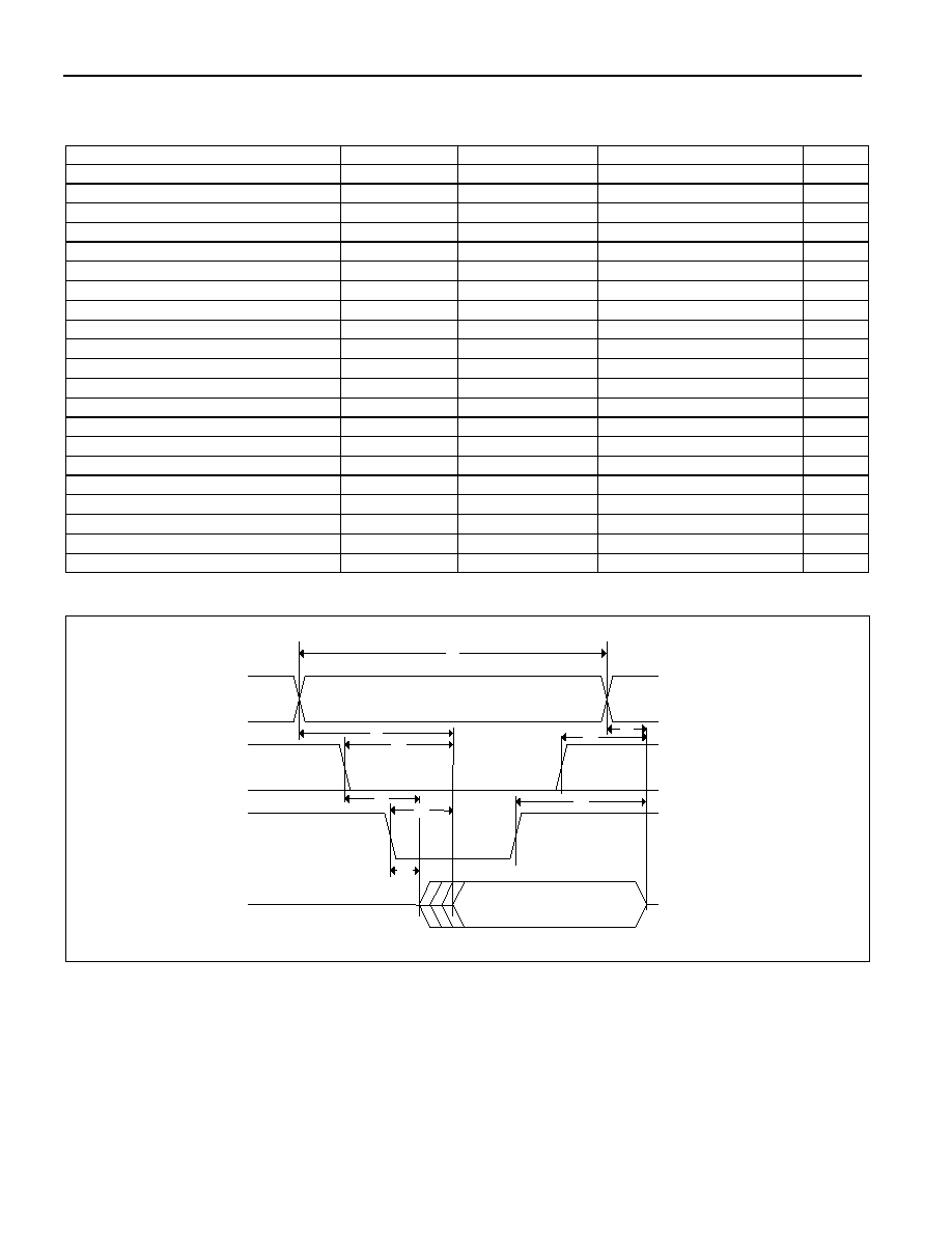
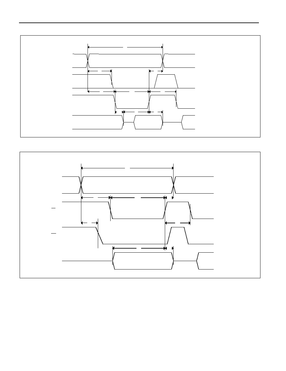
Figure 1. Read Cycle Timing
t
RC
t
CEA
t
OEA
t
CEL
t
OEL
t
OH
t
OEZ
t
AA
VALID
DQ0-DQ7
OE
CE
A0≠A4
t
CEZ
DS1501/DS1511 Y2KC Watchdog Real-Time Clocks
5 of 20
Figure 2. Write Cycle Timing, Write-Enable Controlled
Figure 3. Write Cycle Timing, Chip-Enable Controlled
t
WC
t
AH
t
DS
t
AS
t
WEZ
t
DH
t
WR
t
AS
DATA INPUT
DQ0≠DQ7
WE
CE
A0≠A4
DATA OUTPUT
DATA INPUT
t
WEW
VALID
VALID
t
WC
t
AH
t
DS
t
AS
t
DH
t
WR
t
AS
DATA INPUT
DQ0-DQ7
WE
CE
A0-A4
DATA INPUT
t
CEW
VALID
VALID