1 of 19
043001
FEATURES
∑
Unique 1-wire interface requires only one
port pin for communication
∑
Derives power from data line ("parasite
power")--does not need a local power supply
∑
Multi-drop capability simplifies distributed
temperature sensing applications
∑
Requires no external components
∑ ±
2.0
∞
C accuracy from ≠10∞C to +85∞C
∑
Measures temperatures from ≠55∞C to
+100∞C (≠67∞F to +212∞F)
∑
Thermometer resolution is user-selectable
from 9 to 12 bits
∑
Converts temperature to 12-bit digital word in
750 ms (max.)
∑
User≠definable temperature alarm settings
∑
Alarm search command identifies and
addresses devices whose temperature is
outside of programmed limits (temperature
alarm condition)
∑
Software compatible with the DS18B20-PAR
∑
Ideal for use in remote sensing applications
(e.g., temperature probes) that do not have a
local power source
PIN ASSIGNMENT
PIN DESCRIPTION
GND -
Ground
DQ -
Data
In/Out
NC
- No Connect
DESCRIPTION
The DS1822-PAR digital thermometer provides 9 to 12≠bit centigrade temperature measurements and has
an alarm function with nonvolatile user-programmable upper and lower trigger points. The DS1822-PAR
does not need an external power supply because it derives power directly from the data line ("parasite
power"). The DS1822-PAR communicates over a 1-wire bus, which by definition requires only one data
line (and ground) for communication with a central microprocessor. It has an operating temperature
range of ≠55∞C to +100∞C and is accurate to
±
2.0
∞
C over a range of ≠10∞C to +85∞C.
Each DS1822-PAR has a unique 64-bit identification code, which allows multiple DS1822-PARs to
function on the same 1≠wire bus; thus, it is simple to use one microprocessor to control many
DS1822-PARs distributed over a large area. Applications that can benefit from this feature include
HVAC environmental controls, temperature monitoring systems inside buildings, equipment or
machinery, and process monitoring and control systems.
DS1822-PAR
Econo 1-Wire
Æ
Parasite-Power
Digital Thermometer
www.dalsemi.com
1
(BOTTOM VIEW)
2 3
TO-92
(DS1822-PAR)
DALLAS
1822P
1
GND
DQ
NC
2 3
DS1822-PAR
2 of 19
DETAILED PIN DESCRIPTIONS Table 1
PIN SYMBOL
DESCRIPTION
1 GND
Ground.
2 DQ
Data Input/Output pin. Open-drain 1-wire interface pin. Also provides power
to the device when used in parasite power mode (see "Parasite Power" section.)
3 NC
No Connect. Doesn't connect to internal circuit.
OVERVIEW
The DS1822-PAR uses Dallas' exclusive 1-wire bus protocol that implements bus communication using
one control signal. The control line requires a weak pullup resistor since all devices are linked to the bus
via a 3-state or open-drain port (the DQ pin in the case of the DS1822-PAR). In this bus system, the
microprocessor (the master device) identifies and addresses devices on the bus using each device's unique
64-bit code. Because each device has a unique code, the number of devices that can be addressed on one
bus is virtually unlimited. The 1-wire bus protocol, including detailed explanations of the commands and
"time slots," is covered in the 1-WIRE BUS SYSTEM section of this datasheet.
An important feature of the DS1822-PAR is its ability to operate without an external power supply.
Power is instead supplied through the 1-wire pullup resistor via the DQ pin when the bus is high. The
high bus signal also charges an internal capacitor (C
PP
), which then supplies power to the device when the
bus is low. This method of deriving power from the 1-wire bus is referred to as "parasite power."
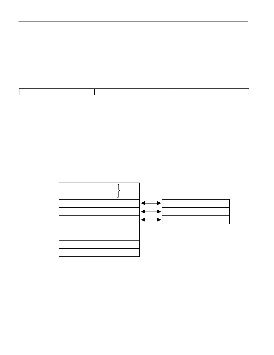
Figure 1 shows a block diagram of the DS1822-PAR, and pin descriptions are given in Table 1. The
64-bit ROM stores the device's unique serial code. The scratchpad memory contains the 2-byte
temperature register that stores the digital output from the temperature sensor. In addition, the scratchpad
provides access to the 1-byte upper and lower alarm trigger registers (T
H
and T
L
). The T
H
and T
L
registers are nonvolatile (EEPROM), so they will retain their data when the device is powered down.
DS1822-PAR BLOCK DIAGRAM Figure 1
C
PP
V
PU
4.7K
64-BIT ROM
AND
1-wire PORT
DQ
INTERNAL V
DD
PARASITE POWER
CIRCUIT
MEMORY CONTROL
LOGIC
SCRATCHPAD
8-BIT CRC GENERATOR
TEMPERATURE SENSOR
ALARM HIGH TRIGGER (T
H
)
REGISTER (EEPROM)
ALARM LOW TRIGGER (T
L
)
REGISTER (EEPROM)
CONFIGURATION REGISTER
(EEPROM)
GND
DS1822-PAR
DS1822-PAR
3 of 19
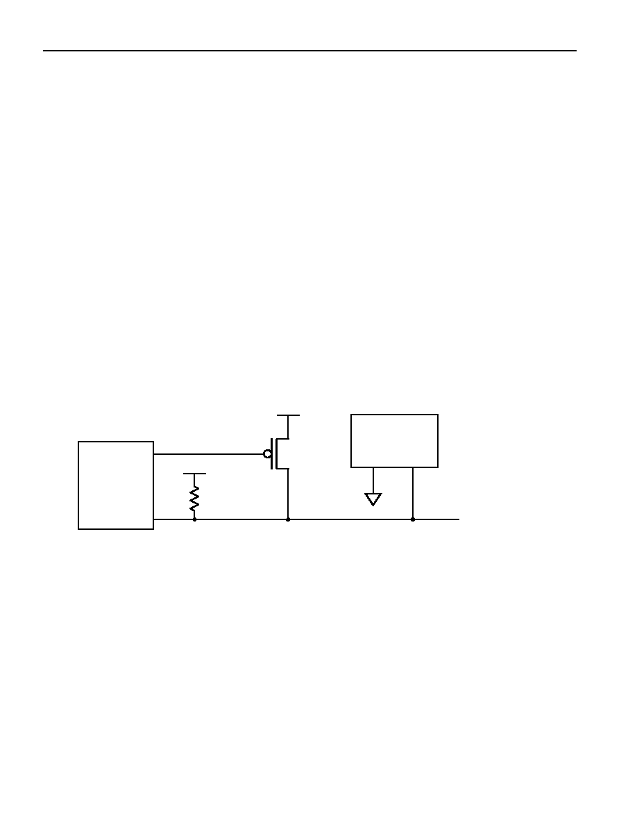
PARASITE POWER
The DS1822-PAR's parasite power circuit allows the DS1822-PAR to operate without a local external
power supply. This ability is especially useful for applications that require remote temperature sensing or
that are very space constrained. Figure 1 shows the DS1822-PAR's parasite-power control circuitry,
which "steals" power from the 1-wire bus via the DQ pin when the bus is high. The stolen charge powers
the DS1822-PAR while the bus is high, and some of the charge is stored on the parasite power capacitor
(C
PP
) to provide power when the bus is low.
The 1-wire bus and C
PP
can provide sufficient parasite power to the DS1822-PAR for most operations as
long as the specified timing and voltage requirements are met (refer to the DC ELECTRICAL
CHARACTERISTICS and the AC ELECTRICAL CHARACTERISTICS sections of this data sheet).
However, when the DS1822-PAR is performing temperature conversions or copying data from the
scratchpad memory to EEPROM, the operating current can be as high as 1.5 mA. This current can cause
an unacceptable voltage drop across the weak 1-wire pullup resistor and is more current than can be
supplied by C
PP
. To assure that the DS1822-PAR has sufficient supply current, it is necessary to provide
a strong pullup on the 1-wire bus whenever temperature conversions are taking place or data is being
copied from the scratchpad to EEPROM. This can be accomplished by using a MOSFET to pull the bus
directly to the rail as shown in Figure 2. The 1-wire bus must be switched to the strong pullup within 10
µ
s (max) after a Convert T [44h] or Copy Scratchpad [48h] command is issued, and the bus must be held
high by the pullup for the duration of the conversion (t
conv
) or data transfer (t
wr
= 10 ms). No other
activity can take place on the 1-wire bus while the pullup is enabled.
SUPPLYING THE DS1822-PAR DURING TEMPERATURE CONVERSIONS
Figure 2
OPERATION ≠ MEASURING TEMPERATURE
The core functionality of the DS1822-PAR is its direct-to-digital temperature sensor. The resolution of
the temperature sensor is user-configurable to 9, 10, 11, or 12 bits, which corresponds to increments of
0.5
∞
C, 0.25
∞
C, 0.125
∞
C, and 0.0625
∞
C, respectively. The default resolution at power-up is 12-bit.
The DS1822-PAR powers-up in a low-power idle state; to initiate a temperature measurement and A-to-D
conversion, the master must issue a Convert T [44h] command. Following the conversion, the resulting
thermal data is stored in the 2-byte temperature register in the scratchpad memory and the DS1822-PAR
returns to its idle state.
The DS1822-PAR output data is calibrated in degrees centigrade; for Fahrenheit
applications, a lookup table or conversion routine must be used. The temperature data is stored as a 16-
bit sign-extended two's complement number in the temperature register (see Figure 3). The sign bits (S)
indicate if the temperature is positive or negative: for positive numbers S = 0 and for negative numbers S
= 1. If the DS1822-PAR is configured for 12-bit resolution, all bits in the temperature register will
contain valid data. For 11-bit resolution, bit 0 is undefined. For 10-bit resolution, bits 1 and 0 are
undefined, and for 9-bit resolution bits 2, 1 and 0 are undefined. Table 2 gives examples of digital output
data and the corresponding temperature reading for 12-bit resolution conversions.
V
PU
V
PU
4.7K
1-Wire Bus
Micro-
processor
DS1822-PAR
GND
DQ
To Other
1-Wire Devices
DS1822-PAR
4 of 19
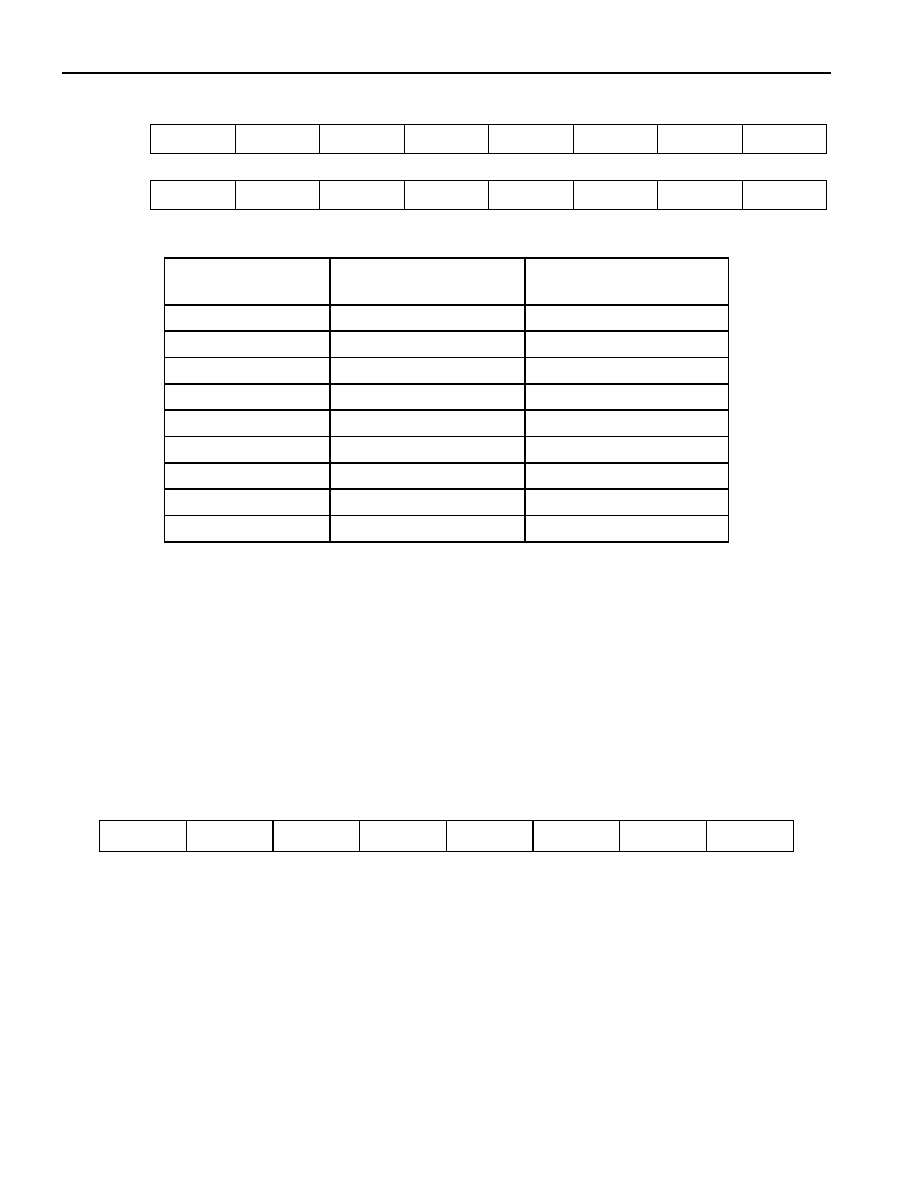
TEMPERATURE REGISTER FORMAT Figure 3
bit 7
bit 6
bit 5
bit 4
bit 3
bit 2
bit 1
bit 0
LS Byte
2
3
2
2
2
1
2
0
2
-1
2
-2
2
-3
2
-4
bit 15
bit 14
bit 13
bit 12
bit 11
bit 10
bit 9
bit 8
MS Byte
S S S S S 2
6
2
5
2
4
TEMPERATURE/DATA RELATIONSHIP Table 2
TEMPERATURE DIGITAL
OUTPUT
(Binary)
DIGITAL OUTPUT
(Hex)
+85∞C*
0000 0101 0101 0000
0550h
+25.0625∞C
0000 0001 1001 0001
0191h
+10.125∞C
0000 0000 1010 0010
00A2h
+0.5∞C
0000 0000 0000 1000
0008h
0∞C
0000 0000 0000 0000
0000h
-0.5∞C
1111 1111 1111 1000
FFF8h
-10.125∞C
1111 1111 0101 1110
FF5Eh
-25.0625∞C
1111 1110 0110 1111
FE6Fh
-55∞C
1111 1100 1001 0000
FC90h
*The power-on reset value of the temperature register is +85∞C
OPERATION ≠ ALARM SIGNALING
After the DS1822-PAR performs a temperature conversion, the temperature value is compared to the
user-defined two's complement alarm trigger values stored in the 1-byte T
H
and T
L
registers (see Figure
4). The sign bit (S)
indicates if the value is positive or negative: for positive numbers S = 0 and for
negative numbers S = 1. The T
H
and T
L
registers are nonvolatile (EEPROM) so they will retain data
when the device is powered down. T
H
and T
L
can be accessed through bytes 2 and 3 of the scratchpad as
explained in the MEMORY section of this datasheet.
T
H
AND T
L
REGISTER FORMAT Figure 4
bit 7
bit 6
bit 5
bit 4
bit 3
bit 2
bit 1
bit 0
S 2
6
2
5
2
5
2
5
2
2
2
1
2
0
Only bits 11 through 4 of the temperature register are used in the T
H
and T
L
comparison since T
H
and T
L
are 8-bit registers. If the result of a temperature measurement is higher than T
H
or lower than T
L
, an
alarm condition exists and an alarm flag is set inside the DS1822-PAR. This flag is updated after every
temperature measurement; therefore, if the alarm condition goes away, the flag will be turned off after the
next temperature conversion.
The master device can check the alarm flag status of all DS1822-PARs on the bus by issuing an Alarm
Search [ECh] command. Any DS1822-PARs with a set alarm flag will respond to the command, so the
master can determine exactly which DS1822-PARs have experienced an alarm condition. If an alarm
condition exists and the T
H
or T
L
settings have changed, another temperature conversion should be done
to validate the alarm condition.
DS1822-PAR
5 of 19
64-BIT LASERED ROM CODE
Each DS1822-PAR contains a unique 64≠bit code (see Figure 5) stored in ROM. The least significant 8
bits of the ROM code contain the DS1822-PAR's 1≠wire family code: 22h. The next 48 bits contain a
unique serial number. The most significant 8 bits contain a cyclic redundancy check (CRC) byte that is
calculated from the first 56 bits of the ROM code. A detailed explanation of the CRC bits is provided in
the CRC GENERATION section. The 64≠bit ROM code and associated ROM function control logic
allow the DS1822-PAR to operate as a 1≠wire device using the protocol detailed in the 1-WIRE BUS
SYSTEM section of this datasheet.
64-BIT LASERED ROM CODE Figure 5
8-BIT CRC
48-BIT SERIAL NUMBER
8-BIT FAMILY CODE (22h)
MEMORY
The DS1822-PAR's memory is organized as shown in Figure 6. The memory consists of an SRAM
scratchpad with nonvolatile EEPROM storage for the high and low alarm trigger registers (T
H
and T
L
)
and configuration register. Note that if the DS1822-PAR alarm function is not used, the T
H
and T
L
registers can serve as general-purpose memory. All memory commands are described in detail in the
DS1822-PAR FUNCTION COMMANDS section.
DS1822-PAR MEMORY MAP
c·÷ÏÍ…=S
SCRATCHPAD (Power-up State)
byte 0 Temperature LSB (50h)
byte 1 Temperature MSB (05h)
EEPROM
byte 2 T
H
Register or User Byte 1*
T
H
Register or User Byte 1
byte 3 T
L
Register or User Byte 2*
T
L
Register or User Byte 2
byte 4 Configuration Register*
Configuration Register
byte 5 Reserved (FFh)
byte 6 Reserved (0Ch)
byte 7 Reserved (10h)
byte 8 CRC*
*
Power-up state depends on value(s) stored
in EEPROM
Byte 0 and byte 1 of the scratchpad contain the LSB and the MSB of the temperature register,
respectively. These bytes are read-only. Bytes 2 and 3 provide access to T
H
and T
L
registers. Byte 4
contains the configuration register data, which is explained in detail in the CONFIGURATION
REGISTER section of this datasheet. Bytes 5, 6 and 7 are reserved for internal use by the device and
cannot be overwritten; these bytes will return all 1s when read.
Byte 8 of the scratchpad is read-only and contains the cyclic redundancy check (CRC) code for bytes 0
through 7 of the scratchpad. The DS1822-PAR generates this CRC using the method described in the
CRC GENERATION section.
MSB MSB
LSB LSB
LSB
MSB
(85∞C)
DS1822-PAR
6 of 19
Data is written to bytes 2, 3, and 4 of the scratchpad using the Write Scratchpad [4Eh] command, and the
data must be transmitted to the DS1822-PAR starting with the least significant bit of byte 2. To verify
data integrity, the scratchpad can be read (using the Read Scratchpad [BEh] command) after the data is
written. When reading the scratchpad, data is transferred over the 1-wire bus starting with the least
significant bit of byte 0. To transfer the T
H
, T
L
and configuration data from the scratchpad to EEPROM,
the master must issue the Copy Scratchpad [48h] command.
Data in the EEPROM registers is retained when the device is powered down; at power-up the EEPROM
data is reloaded into the corresponding scratchpad locations. Data can also be reloaded from EEPROM
to the scratchpad at any time using the Recall E
2
[B8h] command. The master can issue "read time slots"
(see the 1-WIRE BUS SYSTEM section) following the Recall E
2
command and the DS1822-PAR will
indicate the status of the recall by transmitting 0 while the recall is in progress and 1 when the recall is
done.
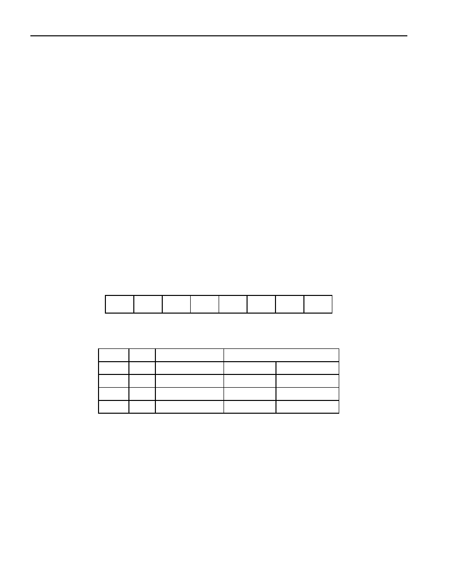
CONFIGURATION REGISTER
Byte 4 of the scratchpad memory contains the configuration register, which is organized as illustrated in
Figure 7. The user can set the conversion resolution of the DS1822-PAR using the R0 and R1 bits in this
register as shown in Table 3. The power-up default of these bits is R0 = 1 and R1 = 1 (12-bit resolution).
Note that there is a direct tradeoff between resolution and conversion time. Bit 7 and bits 0-4 in the
configuration register are reserved for internal use by the device and cannot be overwritten; these bits will
return 1s when read.
CONFIGURATION REGISTER Figure 7
bit 7
bit 6
bit 5
bit 4
bit 3
bit 2
bit 1
bit 0
0 R1
R0 1 1 1 1 1
THERMOMETER RESOLUTION CONFIGURATION Table 3
R1
R0
Resolution
Max Conversion Time
0 0
9-bit
93.75
ms (t
CONV
/8)
0 1
10-bit 187.5
ms (t
CONV
/4)
1 0
11-bit
375
ms (t
CONV
/2)
1 1
12-bit
750
ms (t
CONV
)
CRC GENERATION
CRC bytes are provided as part of the DS1822-PAR's 64-bit ROM code and in the 9
th
byte of the
scratchpad memory. The ROM code CRC is calculated from the first 56 bits of the ROM code and is
contained in the most significant byte of the ROM. The scratchpad CRC is calculated from the data
stored in the scratchpad, and therefore it changes when the data in the scratchpad changes. The CRCs
provide the bus master with a method of data validation when data is read from the DS1822-PAR. To
verify that data has been read correctly, the bus master must re-calculate the CRC from the received data
and then compare this value to either the ROM code CRC (for ROM reads) or to the scratchpad CRC (for
scratchpad reads). If the calculated CRC matches the read CRC, the data has been received error free. The
comparison of CRC values and the decision to continue with an operation are determined entirely by the
DS1822-PAR
7 of 19
bus master. There is no circuitry inside the DS1822-PAR that prevents a command sequence from
proceeding if the DS1822-PAR CRC (ROM or scratchpad) does not match the value generated by the bus
master.
The equivalent polynomial function of the CRC (ROM or scratchpad) is: CRC = X
8
+ X
5
+ X
4
+ 1
The bus master can re-calculate the CRC and compare it to the CRC values from the DS1822-PAR using
the polynomial generator shown in Figure 8. This circuit consists of a shift register and XOR gates, and
the shift register bits are initialized to 0. Starting with the least significant bit of the ROM code or the
least significant bit of byte 0 in the scratchpad, one bit at a time should shifted into the shift register.
After shifting in the 56
th
bit from the ROM or the most significant bit of byte 7 from the scratchpad, the
polynomial generator will contain the re-calculated CRC. Next, the 8-bit ROM code or scratchpad CRC
from the DS1822-PAR must be shifted into the circuit. At this point, if the re-calculated CRC was
correct, the shift register will contain all 0s. Additional information about the Dallas 1-wire cyclic
redundancy check is available in Application Note 27 entitled "Understanding and Using Cyclic
Redundancy Checks with Dallas Semiconductor Touch Memory Products."
CRC GENERATOR Figure 8
1-WIRE BUS SYSTEM
The 1-wire bus system uses a single bus master to control one or more slave devices. The DS1822-PAR
is always a slave. When there is only one slave on the bus, the system is referred to as a "single-drop"
system; the system is "multi-drop" if there are multiple slaves on the bus.
All data and commands are transmitted least significant bit first over the 1-wire bus.
The following discussion of the 1-wire bus system is broken down into three topics: hardware
configuration, transaction sequence, and 1-wire signaling (signal types and timing).
HARDWARE CONFIGURATION
The 1-wire bus has by definition only a single data line. Each device (master or slave) interfaces to the
data line via an open drain or 3≠state port. This allows each device to "release" the data line when the
device is not transmitting data so the bus is available for use by another device. The 1-wire port of the
DS1822-PAR (the DQ pin) is open drain with an internal circuit equivalent to that shown in Figure 9.
The 1-wire bus requires an external pullup resistor of approximately 5 k
; thus, the idle state for the 1-
wire bus is high. If for any reason a transaction needs to be suspended, the bus MUST be left in the idle
state if the transaction is to resume. Infinite recovery time can occur between bits so long as the 1-wire
bus is in the inactive (high) state during the recovery period. If the bus is held low for more than 480
µ
s,
all components on the bus will be reset. In addition, to assure that the DS1822-PAR has sufficient supply
current during temperature conversions, it is necessary to provide a strong pullup (such as a MOSFET) on
the 1-wire bus whenever temperature conversions are taking place (as described in the PARASITE
POWER section).
(MSB)
(LSB)
XOR XOR
XOR
INPUT
DS1822-PAR
8 of 19
HARDWARE CONFIGURATION
c·÷ÏÍ…=V=
TRANSACTION SEQUENCE
The transaction sequence for accessing the DS1822-PAR is as follows:
Step 1. Initialization
Step 2. ROM Command (followed by any required data exchange)
Step 3. DS1822-PAR Function Command (followed by any required data exchange)
It is very important to follow this sequence every time the DS1822-PAR is accessed, as the DS1822-PAR
will not respond if any steps in the sequence are missing or out of order. Exceptions to this rule are the
Search ROM [F0h] and Alarm Search [ECh] commands. After issuing either of these ROM commands,
the master must return to Step 1 in the sequence.
INITIALIZATION
All transactions on the 1-wire bus begin with an initialization sequence. The initialization sequence
consists of a reset pulse transmitted by the bus master followed by presence pulse(s) transmitted by the
slave(s). The presence pulse lets the bus master know that slave devices (such as the DS1822-PAR) are
on the bus and are ready to operate. Timing for the reset and presence pulses is detailed in the
1-WIRE SIGNALING section.
ROM COMMANDS
After the bus master has detected a presence pulse, it can issue a ROM command. These commands
operate on the unique 64≠bit ROM codes of each slave device and allow the master to single out a
specific device if many are present on the 1-wire bus. These commands also allow the master to
determine how many and what types of devices are present on the bus or if any device has experienced an
alarm condition. There are five ROM commands, and each command is 8 bits long. The master device
must issue an appropriate ROM command before issuing a DS1822-PAR function command. A
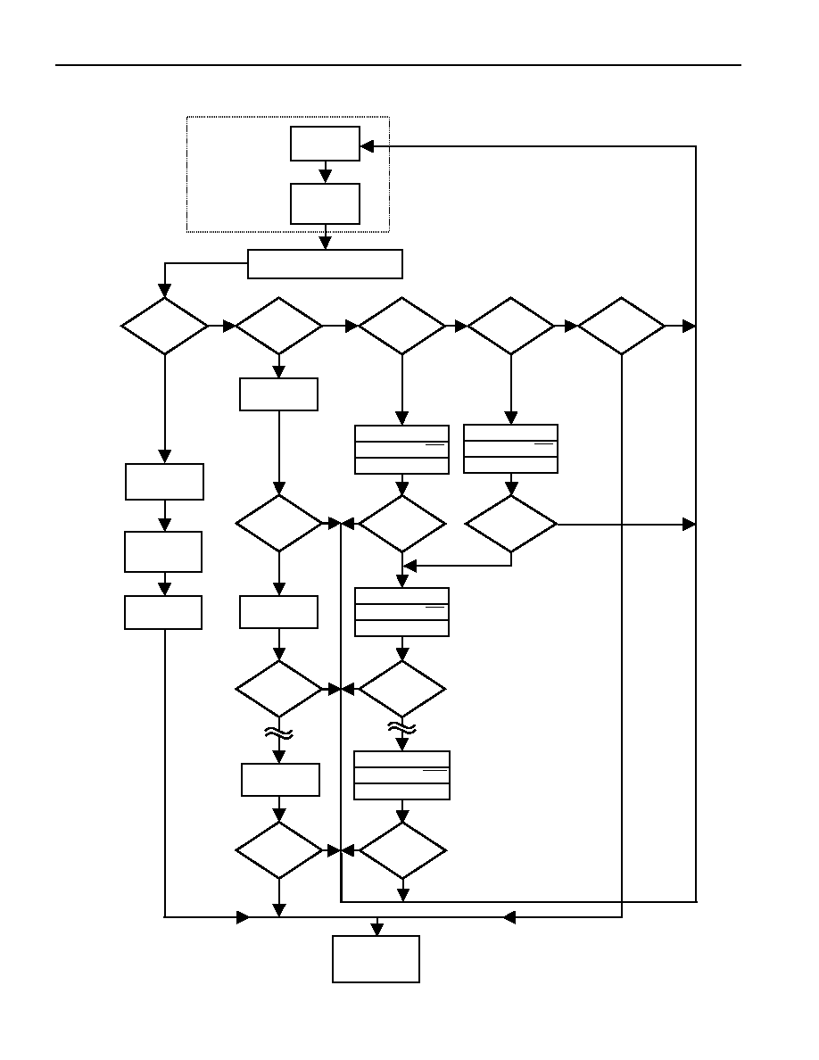
flowchart for operation of the ROM commands is shown in Figure 10.
SEARCH ROM [F0h]
When a system is initially powered up, the master must identify the ROM codes of all slave devices on
the bus, which allows the master to determine the number of slaves and their device types. The master
V
PU
4.7K
5 µA
Typ.
R
X
T
X
DS1822-PAR 1-WIRE PORT
100
MOSFET
T
X
R
X
R
X
= RECEIVE
T
X
= TRANSMIT
1-wire bus
DQ
Pin
V
PU
Micro-
processor
Strong
Pullup

DS1822-PAR
9 of 19
learns the ROM codes through a process of elimination that requires the master to perform a Search ROM
cycle (i.e., Search ROM command followed by data exchange) as many times as necessary to identify all
of the slave devices. If there is only one slave on the bus, the simpler Read ROM command (see below)
can be used in place of the Search ROM process. For a detailed explanation of the Search ROM
procedure, refer to the iButton Book of Standards at www.ibutton.com/ibuttons/standard.pdf. After every
Search ROM cycle, the bus master must return to Step 1 (Initialization) in the transaction sequence.
READ ROM [33h]
This command can only be used when there is one slave on the bus. It allows the bus master to read the
slave's 64-bit ROM code without using the Search ROM procedure. If this command is used when there
is more than one slave present on the bus, a data collision will occur when all the slaves attempt to
respond at the same time.
MATCH ROM [55h]
The match ROM command followed by a 64≠bit ROM code sequence allows the bus master to address a
specific slave device on a multi-drop or single-drop bus. Only the slave that exactly matches the 64≠bit
ROM code sequence will respond to the function command issued by the master; all other slaves on the
bus will wait for a reset pulse.
SKIP ROM [CCh]
The master can use this command to address all devices on the bus simultaneously without sending out
any ROM code information. For example, the master can make all DS1822-PARs on the bus perform
simultaneous temperature conversions by issuing a Skip ROM command followed by a Convert T [44h]
command. Note, however, that the Skip ROM command can only be followed by the Read Scratchpad
[BEh] command when there is one slave on the bus. This sequence saves time by allowing the master to
read from the device without sending its 64≠bit ROM code. This sequence will cause a data collision on
the bus if there is more than one slave since multiple devices will attempt to transmit data simultaneously.
ALARM SEARCH [ECh]
The operation of this command is identical to the operation of the Search ROM command except that
only slaves with a set alarm flag will respond. This command allows the master device to determine if
any DS1822-PARs experienced an alarm condition during the most recent temperature conversion. After
every Alarm Search cycle (i.e., Alarm Search command followed by data exchange), the bus master must
return to Step 1 (Initialization) in the transaction sequence. Refer to the OPERATION ≠ ALARM
SIGNALING section for an explanation of alarm flag operation.
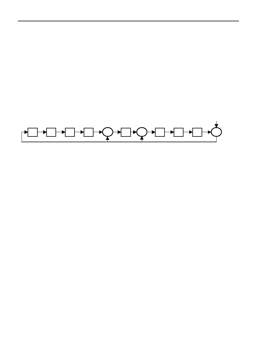
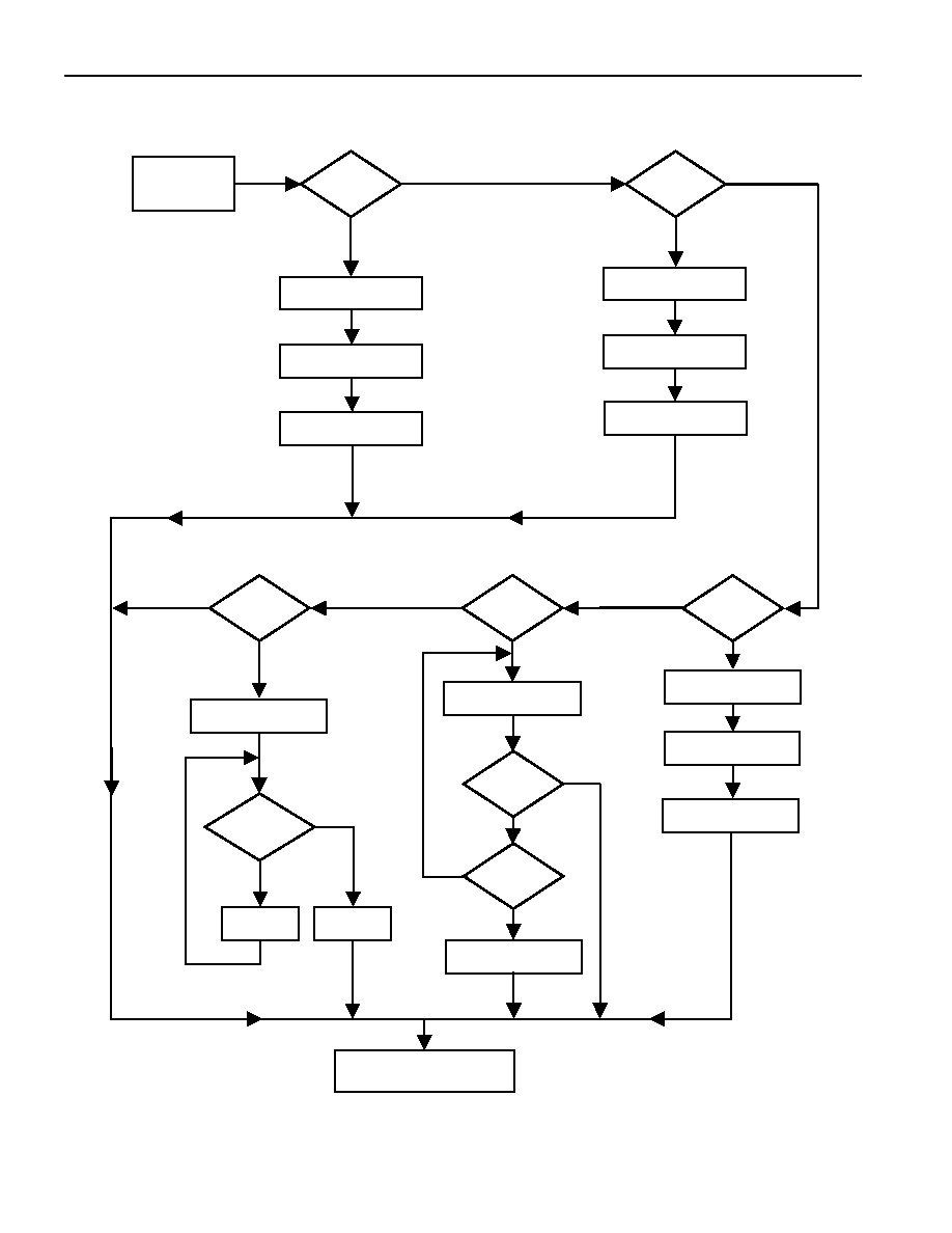
DS1822-PAR FUNCTION COMMANDS
After the bus master has used a ROM command to address the DS1822-PAR with which it wishes to
communicate, the master can issue one of the DS1822-PAR function commands. These commands allow
the master to write to and read from the DS1822-PAR's scratchpad memory, initiate temperature
conversions and determine the power supply mode. The DS1822-PAR function commands, which are
described below, are summarized in Table 4 and illustrated by the flowchart in Figure 10.
CONVERT T [44h]
This command initiates a single temperature conversion. Following the conversion, the resulting thermal
data is stored in the 2-byte temperature register in the scratchpad memory and the DS1822-PAR returns to
its low-power idle state. Within 10
µ
s (max) after this command is issued the master must enable a
strong pullup on the 1-wire bus for the duration of the conversion (t
conv
) as described in the PARASITE
POWER section.
WRITE SCRATCHPAD [4Eh]
This command allows the master to write 3 bytes of data to the DS1822-PAR's scratchpad. The first data
byte is written into the T
H
register (byte 2 of the scratchpad), the second byte is written into the T
L

DS1822-PAR
10 of 19
register (byte 3), and the third byte is written into the configuration register (byte 4). Data must be
transmitted least significant bit first. All three bytes MUST be written before the master issues a reset, or
the data may be corrupted.
READ SCRATCHPAD [BEh]
This command allows the master to read the contents of the scratchpad. The data transfer starts with the
least significant bit of byte 0 and continues through the scratchpad until the 9
th
byte (byte 8 ≠ CRC) is
read. If only part of the scratchpad contents is required, the master may issue a reset to terminate reading
at any time.
COPY SCRATCHPAD [48h]
This command copies the contents of the scratchpad T
H
, T
L
and configuration registers (bytes 2, 3 and 4)
to EEPROM. If the device is being used in parasite power mode, within 10
µ
s (max) after this command
is issued the master must enable a strong pullup on the 1-wire bus for at least 10 ms as described in the
PARASITE POWER section.
RECALL E
2
[B8h]
This command recalls the alarm trigger values (T
H
and T
L
) and configuration data from EEPROM and
places the data in bytes 2, 3, and 4, respectively, in the scratchpad memory. The master device can issue
"read time slots" (see the 1-WIRE BUS SYSTEM section) following the Recall E
2
command and the
DS1822-PAR will indicate the status of the recall by transmitting 0 while the recall is in progress and
1 when the recall is done. The recall operation happens automatically at power-up, so valid data is
available in the scratchpad as soon as power is applied to the device.
DS1822-PAR FUNCTION COMMAND SET Table 4
Command
Description
Protocol
1-Wire Bus Activity
After Command is Issued
Notes
TEMPERATURE CONVERSION COMMANDS
Convert T
Initiates temperature
conversion.
44h None 1
MEMORY COMMANDS
Read Scratchpad
Reads the entire scratchpad
including the CRC byte.
BEh
DS1822-PAR transmits up
to 9 data bytes to master.
2
Write Scratchpad Writes data into scratchpad
bytes 2, 3, and 4 (T
H
, T
L
,
and configuration registers).
4Eh
Master transmits 3 data
bytes to DS1822-PAR.
3
Copy Scratchpad
Copies T
H
, T
L
, and
configuration register data
from the scratchpad to
EEPROM.
48h None 1
Recall E
2
Recalls T
H
, T
L
, and
configuration register data
from EEPROM to the
scratchpad.
B8h DS1822-PAR
transmits
recall status to master.
NOTES:
1. The master must enable a strong pullup on the 1-wire bus during temperature conversions and copies
from the scratchpad to EEPROM. No other bus activity may take place during this time.
2. The master can interrupt the transmission of data at any time by issuing a reset.
3. All three bytes must be written before a reset is issued.
DS1822-PAR
11 of 19
ROM COMMANDS FLOW CHART Figure 9
CCh
SKIP ROM
COMMAND
MASTER T
X
RESET PULSE
DS1822-PAR T
X
PRESENCE
PULSE
MASTER T
X
ROM
COMMAND
33h
READ ROM
COMMAND
55h
MATCH ROM
COMMAND
F0h
SEARCH ROM
COMMAND
ECh
ALARM SEARCH
COMMAND
MASTER T
X
BIT 0
BIT 0
MATCH?
MASTER T
X
BIT 1
BIT 1
MATCH?
BIT 63
MATCH?
MASTER T
X
BIT 63
N
Y
Y Y
Y
Y
N N
N
N
N
N
N
Y
Y
Y
BIT 0
MATCH?
BIT 1
MATCH?
BIT 63
MATCH?
N
N
N
Y
Y
Y
DS1822-PAR T
X
FAMILY CODE
1 BYTE
DS1822-PAR T
X
SERIAL NUMBER
6 BYTES
DS1822-PAR T
X
CRC BYTE
DS1822-PAR T
X
BIT 0
DS1822-PAR T
X
BIT 0
MASTER T
X
BIT 0
N
Y
DEVICE(S)
WITH ALARM
FLAG SET?
Initialization
Sequence
MASTER T
X
FUNCTION
COMMAND
(FIGURE 10)
DS1822-PAR T
X
BIT 0
DS1822-PAR T
X
BIT 0
MASTER T
X
BIT 0
DS1822-PAR T
X
BIT 1
DS1822-PAR T
X
BIT 1
MASTER T
X
BIT 1
DS1822-PAR T
X
BIT 63
DS1822-PAR T
X
BIT 63
MASTER T
X
BIT 63
DS1822-PAR
12 of 19
DS1822-PAR FUNCTION COMMANDS FLOW CHART Figure 10
MASTER T
X
FUNCTION
COMMAND
Y
N
44h
CONVERT
TEMPERATURE
?
MASTER ENABLES
STRONG PULLUP ON DQ
DS1822-PAR CONVERTS
TEMPERATURE
MASTER DISABLES
STRONG PULLUP
Y
N
48h
COPY
SCRATCHPAD
?
MASTER ENABLES
STRONG PULL-UP ON DQ
DATA COPIED FROM
SCRATCHPAD TO EEPROM
MASTER DISABLES
STRONG PULLUP
RETURN TO INITIALIZATION
SEQUENCE (FIGURE 9) FOR
NEXT TRANSACTION
Y
N
Y
BEh
READ
SCRATCHPAD
?
HAVE 8 BYTES
BEEN READ
?
N
MASTER
T
X
RESET
?
MASTER R
X
DATA BYTE
FROM SCRATCHPAD
N
Y
MASTER R
X
SCRATCHPAD
CRC BYTE
MASTER
R
X
"1s"
Y
N
B8h
RECALL E
2
?
MASTER BEGINS DATA
RECALL FROM E
2
PROM
DEVICE
BUSY RECALLING
DATA
?
N
Y
MASTER
R
X
"0s"
MASTER T
X
T
H
BYTE
TO SCRATCHPAD
Y
N
4Eh
WRITE
SCRATCHPAD
?
MASTER T
X
T
L
BYTE
TO SCRATCHPAD
MASTER T
X
CONFIG. BYTE
TO SCRATCHPAD
DS1822-PAR
13 of 19
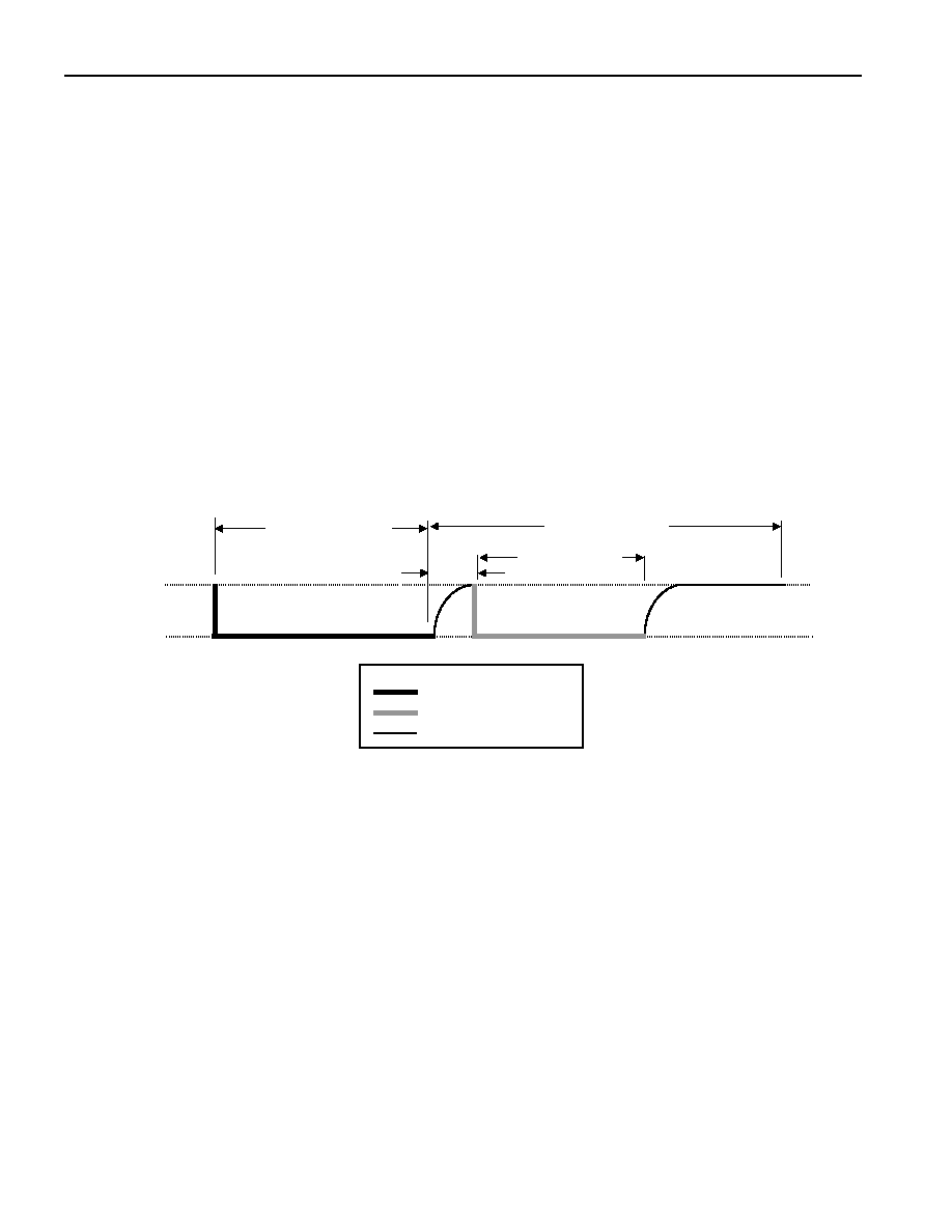
1-WIRE SIGNALING
The DS1822-PAR uses a strict 1-wire communication protocol to insure data integrity. Several signal
types are defined by this protocol: reset pulse, presence pulse, write 0, write 1, read 0, and read 1. All of
these signals, with the exception of the presence pulse, are initiated by the bus master.
INITIALIZATION PROCEDURE: RESET AND PRESENCE PULSES
All communication with the DS1822-PAR begins with an initialization sequence that consists of a reset
pulse from the master followed by a presence pulse from the DS1822-PAR. This is illustrated in
Figure 11. When the DS1822-PAR sends the presence pulse in response to the reset, it is indicating to the
master that it is on the bus and ready to operate.
During the initialization sequence the bus master transmits (T
X
) the reset pulse by pulling the 1-wire bus
low for a minimum of 480
µ
s. The bus master then releases the bus and goes into receive mode (R
X
).
When the bus is released, the 5k pullup resistor pulls the 1-wire bus high. When the DS1822-PAR
detects this rising edge, it waits 15≠60
µ
s and then transmits a presence pulse by pulling the 1-wire bus
low for 60≠240
µ
s.
INITIALIZATION TIMING Figure 11
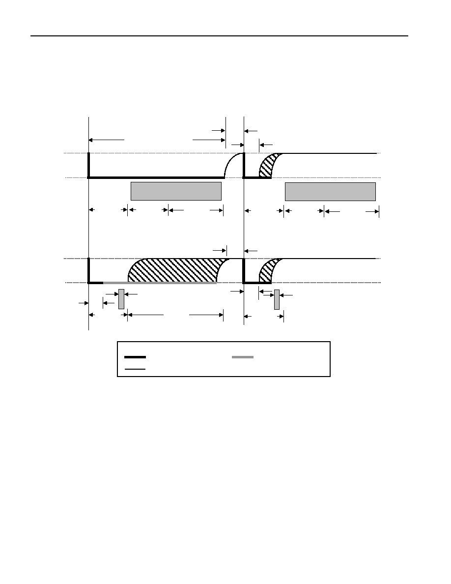
READ/WRITE TIME SLOTS
The bus master writes data to the DS1822-PAR during write time slots and reads data from the DS1822-
PAR during read time slots. One bit of data is transmitted over the 1-wire bus per time slot.
WRITE TIME SLOTS
There are two types of write time slots: "Write 1" time slots and "Write 0" time slots. The bus master
uses a Write 1 time slot to write a logic 1 to the DS1822-PAR and a Write 0 time slot to write a logic 0 to
the DS1822-PAR. All write time slots must be a minimum of 60
µ
s in duration with a minimum of a 1
µ
s
recovery time between individual write slots. Both types of write time slots are initiated by the master
pulling the 1-wire bus low (see Figure 12).
To generate a Write 1 time slot, after pulling the 1-wire bus low, the bus master must release the 1-wire
bus within 15
µ
s. When the bus is released, the 5k pullup resistor will pull the bus high. To generate a
Write 0 time slot, after pulling the 1-wire bus low, the bus master must continue to hold the bus low for
the duration of the time slot (at least 60
µ
s).
LINE TYPE LEGEND
Bus master pulling low
DS1822-PAR pulling low
Resistor pullup
V
PU
GND
1-WIRE BUS
480
µ
µ
µ
µ
s minimum
480
µ
µ
µ
µ
s minimum
DS1822-PAR T
X
presence pulse
60-240
µ
µ
µ
µ
s
MASTER T
X
RESET PULSE
MASTER R
X
DS1822-PAR
waits 15-60
µ
µ
µ
µ
s
DS1822-PAR
14 of 19
The DS1822-PAR samples the 1-wire bus during a window that lasts from 15
µ
s to 60
µ
s after the master
initiates the write time slot. If the bus is high during the sampling window, a 1 is written to the DS1822-
PAR. If the line is low, a 0 is written to the DS1822-PAR.
READ/WRITE TIME SLOT TIMING DIAGRAM Figure 12
READ TIME SLOTS
The DS1822-PAR can only transmit data to the master when the master issues read time slots. Therefore,
the master must generate read time slots immediately after issuing a Read Scratchpad [BEh] command, so
that the DS1822-PAR can provide the requested data. In addition, the master can generate read time slots
after issuing a Recall E
2
[B8h] command to find out the recall status as explained in the DS1822-PAR
FUNCTION COMMAND section.
All read time slots must be a minimum of 60
µ
s in duration with a minimum of a 1
µ
s recovery time
between slots. A read time slot is initiated by the master device pulling the 1-wire bus low for a
minimum of 1
µ
s and then releasing the bus (see Figure 12). After the master initiates the read time slot,
the DS1822-PAR will begin transmitting a 1 or 0 on bus. The DS1822-PAR transmits a 1 by leaving the
bus high and transmits a 0 by pulling the bus low. When transmitting a 0, the DS1822-PAR will release
the bus by the end of the time slot, and the bus will be pulled back to its high idle state by the pullup
LINE TYPE LEGEND
Bus master pulling low
DS1822-PAR pulling low
Resistor
pullup
45
µ
µ
µ
µ
s
15
µ
µ
µ
µ
s
V
PU
GND
1-WIRE BUS
60
µ
µ
µ
µ
s < T
X
"0" < 120
1
µ
µ
µ
µ
s < T
REC
<
DS1822-PAR samples
MIN TYP MAX
15
µ
µ
µ
µ
s
30
µ
µ
µ
µ
s
> 1
µ
µ
µ
µ
s
MASTER WRITE "0" SLOT
MASTER WRITE "1" SLOT
DS1822-PAR samples
MIN TYP MAX
V
PU
GND
1-WIRE BUS
15
µ
µ
µ
µ
s
MASTER READ "0" SLOT
MASTER READ "1" SLOT
Master samples
Master samples
START
OF SLOT
START
OF SLOT
> 1
µ
µ
µ
µ
s
1
µ
µ
µ
µ
s < T
REC
<
15
µ
µ
µ
µ
s
15
µ
µ
µ
µ
s
30
µ
µ
µ
µ
s
15
µ
µ
µ
µ
s
> 1
µ
µ
µ
µ
s
DS1822-PAR
15 of 19
resister. Output data from the DS1822-PAR is valid for 15
µ
s after the falling edge that initiated the read
time slot. Therefore, the master must release the bus and then sample the bus state within 15
µ
s from the
start of the slot.
Figure 13 illustrates that the sum of T
INIT
, T
RC
, and T
SAMPLE
must be less than 15
µ
s for a read time slot.
Figure 14 shows that system timing margin is maximized by keeping T
INIT
and T
RC
as short as possible
and by locating the master sample time during read time slots towards the end of the 15
µ
s period.
DETAILED MASTER READ 1 TIMING Figure 13
RECOMMENDED MASTER READ 1 TIMING Figure 14
RELATED APPLICATION NOTES
The following Application Notes can be applied to the DS1822-PAR. These notes can be obtained from
the Dallas Semiconductor "Application Note Book," via the Dallas website at
http://www.dalsemi.com/
,
or through our faxback service at (214) 450≠0441.
Application Note 27: "Understanding and Using Cyclic Redundancy Checks with Dallas Semiconductor
Touch Memory Product"
Application Note 55: "Extending the Contact Range of Touch Memories"
Application Note 74: "Reading and Writing Touch Memories via Serial Interfaces"
Application Note 104: "Minimalist Temperature Control Demo"
Application Note 106: "Complex MicroLANs"
Application Note 108: "MicroLAN ≠ In the Long Run"
Sample 1-wire subroutines that can be used in conjunction with AN74 can be downloaded from the
Dallas website or anonymous FTP Site.
V
PU
GND
1-WIRE BUS
15
µ
µ
µ
µ
s
VIH of Master
T
RC
T
INT
> 1
µ
µ
µ
µ
s
Master samples
LINE TYPE LEGEND
Bus master pulling low
Resistor pullup
V
PU
GND
1-WIRE BUS
15
µ
µ
µ
µ
s
VIH of Master
T
RC
=
small
T
INT
=
small
Master samples

DS1822-PAR
16 of 19
DS1822-PAR OPERATION EXAMPLE 1
In this example there are multiple DS1822-PARs on the bus. The bus master initiates a temperature
conversion in a specific DS1822-PAR and then reads its scratchpad and recalculates the CRC to verify
the data.
MASTER MODE
DATA (LSB FIRST)
COMMENTS
TX
Reset
Master issues reset pulse.
RX
Presence
DS1822-PARs respond with presence pulse.
TX
55h
Master issues Match ROM command.
TX
64-bit ROM code
Master sends DS1822-PAR ROM code.
TX
44h
Master issues Convert T command.
TX
DQ line held high by
strong pullup
Master applies strong pullup to DQ for the duration of the
conversion (t
conv
).
TX
Reset
Master issues reset pulse.
RX
Presence
DS1822-PARs respond with presence pulse.
TX
55h
Master issues Match ROM command.
TX
64-bit ROM code
Master sends DS1822-PAR ROM code.
TX
BEh
Master issues Read Scratchpad command.
RX
9 data bytes
Master reads entire scratchpad including CRC. The master
then recalculates the CRC of the first eight data bytes from the
scratchpad and compares the calculated CRC with the read
CRC (byte 9). If they match, the master continues; if not, the
read operation is repeated.
DS1822-PAR OPERATION EXAMPLE 2
In this example there is only one DS1822-PAR on the bus. The master writes to the T
H
, T
L
, and
configuration registers in the DS1822-PAR scratchpad and then reads the scratchpad and recalculates the
CRC to verify the data. The master then copies the scratchpad contents to EEPROM.
MASTER MODE
DATA (LSB FIRST)
COMMENTS
TX
Reset
Master issues reset pulse.
RX
Presence
DS1822-PAR responds with presence pulse.
TX
CCh
Master issues Skip ROM command.
TX
4Eh
Master issues Write Scratchpad command.
TX
3 data bytes
Master sends three data bytes to scratchpad (T
H
, T
L
, and config).
TX
Reset
Master issues reset pulse.
RX
Presence
DS1822-PAR responds with presence pulse.
TX
CCh
Master issues Skip ROM command.
TX
BEh
Master issues Read Scratchpad command.
RX
9 data bytes
Master reads entire scratchpad including CRC. The master then
recalculates the CRC of the first eight data bytes from the
scratchpad and compares the calculated CRC with the read CRC
(byte 9). If they match, the master continues; if not, the read
operation is repeated.
TX
Reset
Master issues reset pulse.
RX
Presence
DS1822-PAR responds with presence pulse.
TX
CCh
Master issues Skip ROM command.
TX
48h
Master issues Copy Scratchpad command.
TX
DQ line held high by
strong pullup
Master applies strong pullup to DQ for at least 10 ms while copy
operation is in progress.
DS1822-PAR
17 of 19
ABSOLUTE MAXIMUM RATINGS*
Voltage on any pin relative to ground
≠0.5V to +6.0V
Operating temperature
≠55
∞
C to +100
∞
C
Storage temperature
≠55
∞
C to +125
∞
C
Soldering temperature
See J-STD-020A Specification
*These are stress ratings only and functional operation of the device at these or any other conditions
above those indicated in the operation sections of this specification is not implied. Exposure to absolute
maximum rating conditions for extended periods of time may affect reliability.
DC ELECTRICAL CHARACTERISTICS
(-55∞C to +100∞C; V
PU
=3.0V to 5.5V)
PARAMETER SYMBOL
CONDITION
MIN
TYP
MAX
UNITS
NOTES
Pullup Supply
Voltage
V
PU
3.0
5.5
V
1,2
Thermometer Error
t
ERR
-10∞C to +85∞C
±2
∞C
3
-55∞C to +100∞C
±3
Input Logic Low
V
IL
-0.3
+0.8
V
1,4,5
Input Logic High
V
IH
3.0
5.5
V
1,6
Sink Current
I
L
V
I/O
=0.4V 4.0
mA 1
Active Current
I
DQA
1
1.5
mA
7
DQ Input Current
I
DQ
5
µA
8
Drift
±0.2 ∞C
9
NOTES:
1. All voltages are referenced to ground.
2. The Pullup Supply Voltage specification assumes that the pullup device (resistor or transistor) is
ideal, and therefore the high level of the pullup is equal to V
PU
. In order to meet the V
IH
spec of the
DS1822-PAR, the actual supply rail for the strong pullup transistor must include margin for the
voltage drop across the transistor when it is turned on; thus: V
PU_ACTUAL
= V
PU_IDEAL
+ V
TRANSISTOR
.
3. See typical performance curve in Figure 15.
4. Logic low voltages are specified at a sink current of 4 mA.
5. To always guarantee a presence pulse under low voltage parasite power conditions, V
ILMAX
may have
to be reduced to as low as 0.5V.
6. Logic high voltages are specified at a source current of 1 mA.
7. Active current refers to supply current during active temperature conversions or EEPROM writes.
8. DQ line is high ("hi-Z" state).
9. Drift data is based on a 1000 hour stress test at 125∞C.
AC ELECTRICAL CHARACTERISTICS: NV MEMORY
(-55∞C to +100∞C; V
PU
=3.0V to 5.5V)
PARAMETER SYMBOL
CONDITION
MIN
TYP
MAX
UNITS
NV Write Cycle Time
t
wr
2
10
ms
EEPROM Writes
N
EEWR
-55∞C to +55∞C
50k
writes
EEPROM Data Retention
t
EEDR
-55∞C to +55∞C
10
years

DS1822-PAR
18 of 19
AC ELECTRICAL CHARACTERISTICS: (-55∞C to +100∞C; V
PU
=3.0V to 5.5V)
PARAMETER SYMBOL
CONDITION
MIN
TYP
MAX
UNITS
NOTES
t
CONV
9-bit
resolution 93.75 ms 1
10-bit
resolution
187.5
ms 1
11-bit
resolution
375 ms 1
Temperature Conversion
Time
12-bit
resolution
750 ms 1
Time to Strong Pullup
On
t
SPON
Start Convert T
Command Issued
10 µs
Time Slot
t
SLOT
60
120
µs
1
Recovery Time
t
REC
1
µs
1
Write 0 Low Time
r
LOW0
60
120
µs
1
Write 1 Low Time
t
LOW1
1
15
µs
1
Read Data Valid
t
RDV
15
µs
1
Reset Time High
t
RSTH
480
µs
1
Reset Time Low
t
RSTL
480
960
µs
1,2
Presence Detect High
t
PDHIGH
15
60
µs
1
Presence Detect Low
t
PDLOW
60
240
µs
1
Capacitance C
IN/OUT
25
pF
NOTES:
1. Refer to timing diagrams in Figure 16.
2. If t
RSTL
> 960
µ
s, a power on reset may occur.
TYPICAL PERFORMANCE CURVE Figure 15
DS1822-PAR DIGITAL THERMOMETER AND THERMOSTAT
TEMPERATURE READING ERROR
"TBA"
DS1822-PAR
19 of 19
TIMING DIAGRAMS Figure 16