 | ÐлекÑÑоннÑй компоненÑ: DS1830U | СкаÑаÑÑ:  PDF PDF  ZIP ZIP |
Äîêóìåíòàöèÿ è îïèñàíèÿ www.docs.chipfind.ru
DS1830/A DS183
Note: Some revisions of this device may incorporate deviations from published specifications known as errata. Multiple revisions of any
device may be simultaneously available through various sales channels. For information about device errata, click here:
http://dbserv.maxim-
ic.com/errata.cfm
.
1 of 7
060303
FEATURES
§ 5V (DS1830) or 3.3V (DS1830A) power-on
reset
§ Excellent for systems that need power-on
resets in a consistent sequence
§ Asserts resets during power transients
§ Pushbutton reset input for system override
§ Selectable reset timing
§ Reduces need for discrete components
§ Precision temperature-compensated voltage
reference
§ 8-pin DIP, 8-pin SO, or space saving 8-pin
µSOP
§ Operating temperature of -40°C to +85°C
§ Open-drain, active-low inputs
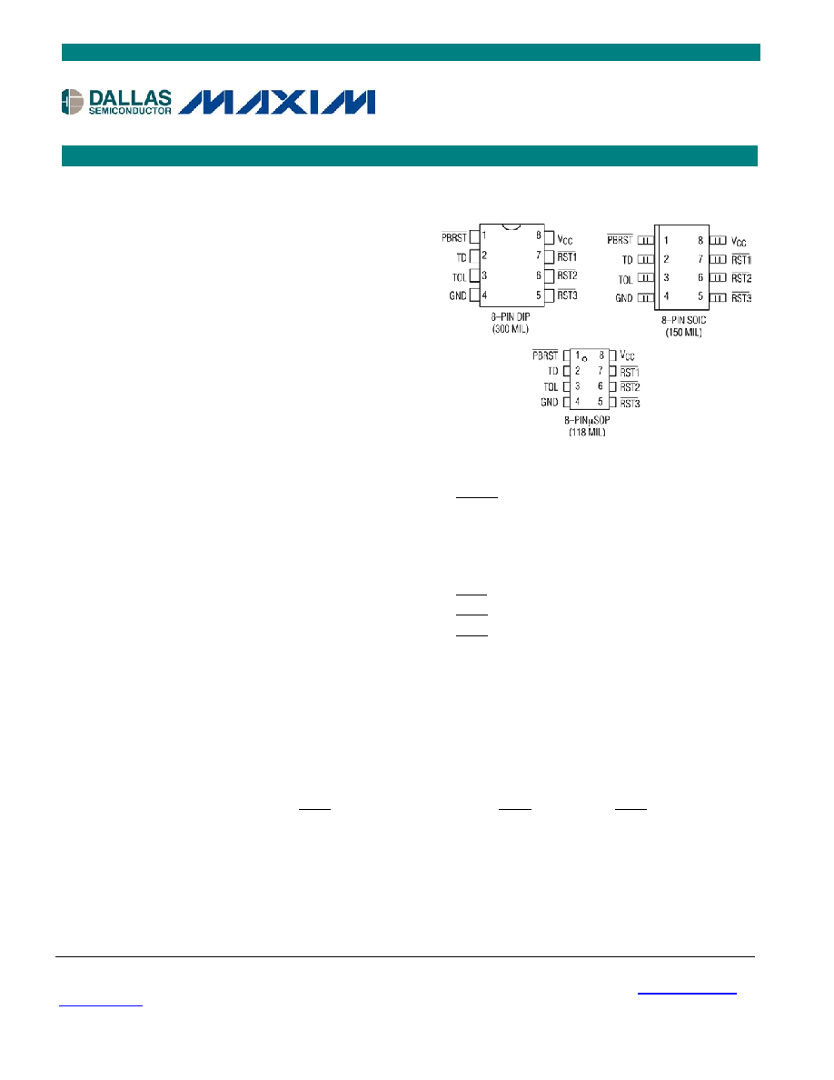
PIN ASSIGNMENT
PIN DESCRIPTION
1
PBRST
- Pushbutton Reset Input
2 TD
- Time Delay Select Input
3 TOL
- V
CC
Tolerance Select Input
4 GND
- Ground
8 V
CC
- Power Supply
7
RST1
- Reset 1 Output
6
RST2
- Reset 2 Output
5
RST3
- Reset 3 Output
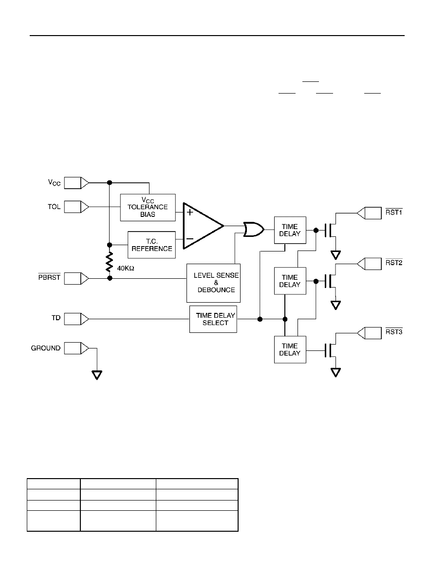
DESCRIPTION
The DS1830 Reset Sequencer monitors the power supply for an in-tolerance condition and the pushbutton
reset input for a manual reset. First a precision temperature-compensated reference and comparator circuit
monitors the status of the power supply and when an out-of-tolerance condition is detected, an internal
power fail signal is generated that forces the reset lines to go to an active state. If the power supply
returns to an in-tolerance condition,
RST1
will release followed by
RST2
and finally
RST3
. Sequencing of
resets allows for systems to power-up in an orderly manner providing superior reliability.
www.maxim-ic.com
DS1830/A
Reset Sequence Pushbutton
D1830/A
2 of 7
OPERATION -- POWER MONITOR
The DS1830 provides the functions of detecting out-of-tolerance conditions on a power supply and
warning a processor based system of impending power failure. When V
CC
is detected as out-of-tolerance
all reset outputs will be forced active. When V
CC
returns to a valid state,
RST1
will remain active for
period of time based on the condition of the TD input. Reset outputs
RST2
and
RST3
follow
RST1
, each
one at the proper delays for the condition of the TD input. All resets will remain in the inactive state
(high) until the next V
CC
out-of-tolerance condition or pushbutton reset. On power-up all resets are kept
active for an appropriate period determined by the status of the TD input after the power supply inputs
have reached the selected tolerance. This allows the power supply and system power to stabilize before
the reset sequences are released.
BLOCK DIAGRAM Figure 1
OPERATION -- TOLERANCE SELECT
The DS1830/A provides a TOL input for individual customization of the DS1830x to specific application
requirements (see Table 1). For the tolerance selection, see Table 1 below. The TOL input is only
sampled while V
CC
is below the lowest potential trip value and can not be changed after the V
CC
voltage
exceeds the lowest potential trip value.
TOL -- TOLERANCE SELECT Table 1
TOL
5V (DS1830)
3.3V (DS1830A)
V
CC
5%
5%
GND
10%
10%
OPEN
(N.C.)
15%
20%
D1830/A
3 of 7
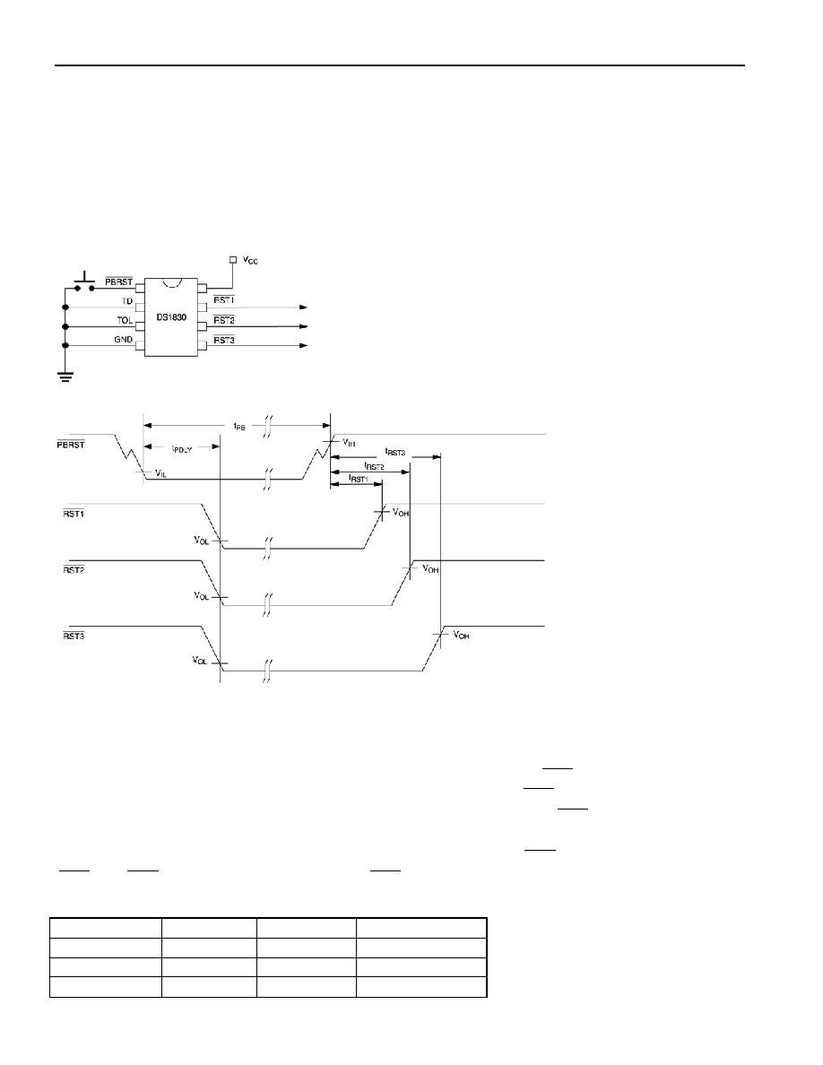
OPERATION -- PUSHBUTTON RESET
The DS1830 provides a pushbutton switch for manual reset control. When any of the DS1830/A resets
are not active (low) a reset cycle can be initiated by a pushbutton reset. The pushbutton reset is generated
by pulling the PBRST pin low for at least 1ms. When the push- button is held low all resets are forced
active. The reset will remain active until the pushbutton input is released and then will start a sequenced
time-out based on the condition of the TD input. The Pushbutton input is pulled high through an internal
40k
W pull-up resistor and debounced via internal circuitry. See Figure 2 for an application example and
Figure 3 for the timing diagram.
PUSHBUTTON RESET Figure 2
TIMING DIAGRAM -- PUSHBUTTON RESET Figure 3
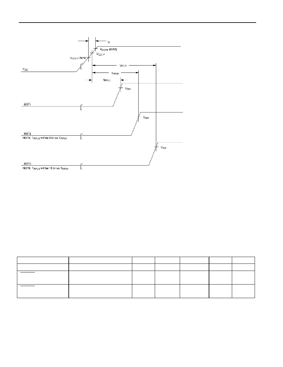
OPERATION -- TIME DELAY SELECT
The DS1830 provides an input to select three time delay characteristics for the reset outputs. The TD
input has 3 states high (V
CC
), low (ground) and no connect (N.C.). Table 2 details the minimum timing
based on the state of the TD input. If the TD input is connected to ground;
RST1
will have a minimum
time delay of 10 ms after V
CC
is in tolerance. If the TD input is floated;
RST1
will have a minimum time
delay of 20 ms after V
CC
is in tolerance. If the TD input is connected to V
CC
,
RST1
will have a minimum
time delay of 50 ms after V
CC
is in tolerance. An oscillator and clock chain generate the reset timing with
each time delay based on the same device oscillator. The time delay for
RST2
will be 5 times as long as
RST1
and
RST3
will be 10 times the duration of
RST1
.
TD CONTROL MINIMUM RESET TIMING Table 2
TD
T
RST1
T
RST2
T
RST3
TD = GND
10ms
50ms
100ms
TD = N.C.
20ms
100ms
200ms
TD = V
CC
50ms
250ms
500ms
D1830/A
4 of 7
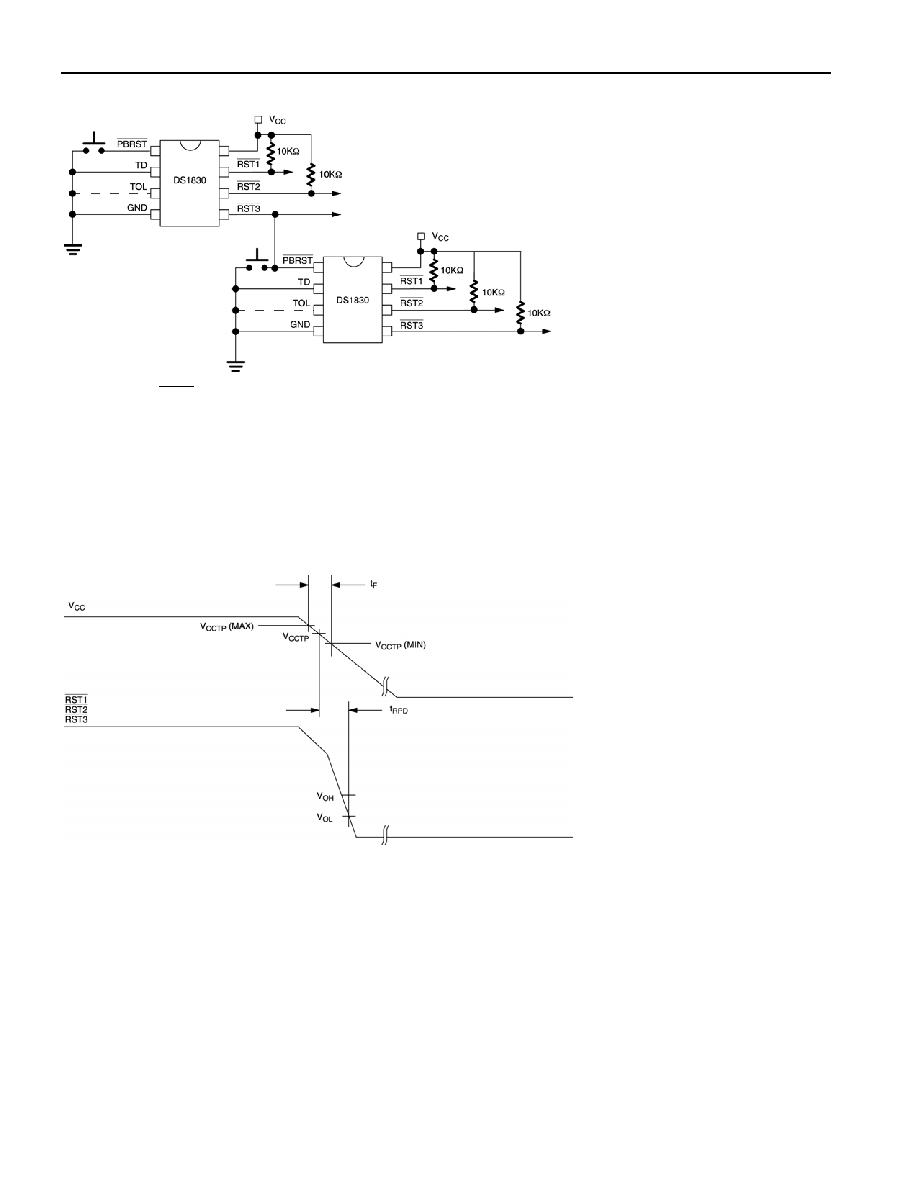
APPLICATION DIAGRAM -- CASCADE DELAY CONFIGURATIONS Figure 4
Note 1: The
RST3
output tied to the pushbutton reset would be pulled to V
CC
through the 40k
W resistor in
the pushbutton input. If a stronger pull-up is required an additional pull-up resistor could be added.
Note 2: When using the cascade configuration, it is important that the TOL pins of the master and the
slave are configured so that the master's V
CCTP
is greater than the slave's V
CCTP
. This will ensure that
when the master's higher V
CCTP
is crossed, the resets will ripple through to the slave.
TIMING DIAGRAM -- POWER-DOWN Figure 5
MASTER
SLAVE
SEE NOTE 2
SEE NOTE 2
SEE NOTE 1
D1830/A
5 of 7
TIMING DIAGRAM -- POWER-UP Figure 6
ABSOLUTE MAXIMUM RATINGS*
Voltage on any Pin Relative to
Ground
-0.5V to +6.0V
Operating Temperature
-40°C to +85°C
Storage Temperature
-55°C to +125°C
Soldering Temperature
See IPC/JEDEC J-STD-020A
* This is a stress rating only and functional operation of the device at these or any other conditions above
those indicated in the operation sections of this specification is not implied. Exposure to absolute
maximum rating conditions for extended periods of time may affect reliability.
RECOMMENDED DC OPERATING CONDITIONS (-40°C to +85°C)
PARAMETER
SYMBOL
MIN
TYP
MAX
UNITS NOTES
Supply Voltage
V
CC
1.0
5.5
V
1
PBRST
Input High
Level
V
IH
2.0
V
CC
+ 0.3
V
PBRST
Input Low
Level
V
IL
-0.3
+0.5
V