1 of 14
051100
FEATURES
2.5V power-on reset
3.3 (or 3V) power-on reset
2 referenced comparators with separate
outputs for monitoring additional supplies
Internal power is drawn from higher of either
the IN
2.5V
input or the IN
3.3V
input
Excellent for systems designed to operate
with multiple power supplies
Asserts resets during power transients
Pushbutton reset input for system override
Maintains reset for user configurable times
of 10 ms, 100 ms, or 1 sec
Watchdog timer for software monitoring
(DS1831D)
Precision temperature-compensated voltage
reference and voltage sensor
16 pin DIP & 16 pin 150 mil SOIC available
Operating Temperature of -40�C to +85�C
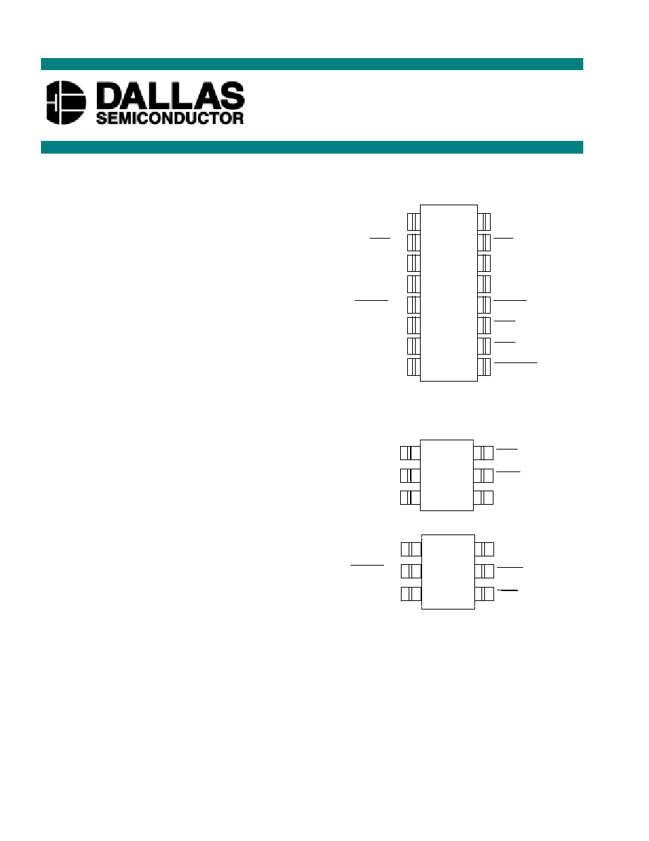
PIN ASSIGNMENT
DESCRIPTION
The DS1831C Multi-Supply Monitor & Reset monitors up to 4 system voltages: 2.5 volt supply, 3.3 (or
3) volt supply, and 2 additional user configurable voltage monitors. DS1831 power for internal operation
comes from the higher voltage level of the 3.3 volt input or the 2.5 volt input. One of these inputs must
be greater than 1 volt for device operation. Pushbutton (manual reset) functionality is provided for the
2.5 volt reset, the 3.3 volt reset or for all reset outputs by the master pushbutton. The DS1831D replaces
one reference comparator and the master pushbutton with watchdog and the DS1831E replaces the
3.3-volt PBRST with a last reset status output.
TOL and TD inputs allow user configuration of the DS1831 for multiple applications. The TOL inputs
configure the tolerance for the specified output and the TD inputs configure the reset time delays.
DS1831C/D/E
3.3V/2.5V Multi-Supply MicroMonitor
www.dalsemi.com
1
2
3
4
5
6
7
8
16
15
14
13
12
11
10
9
IN
3.3V
RST
3.3V
TOL
3.3V
TD
3.3V
PBRST
3.3V
NMI1
NMI2
MPBRST
IN
2.5V
RST
2.5V
TOL
2.5V
TD
2.5V
PBRST
2.5V
IN1
IN2
GND
DS1831C
16-Pin (300 mil) DIP
&
16-Pin (150 mil) SOIC
6
7
8
11
10
9
NMI1
WDS
TD
WD
IN1
ST
GND
DS1831D
4
5
6
13
12
11
TD
3.3V
PBST
NMI1
TD
2.5V
PBRST
2.5V
IN1
DS1831E

DS1831C/D/E
2 of 14
PIN CONFIGURATION
1
IN
2.5V
2.5V Power Supply Input
9
MPBRST
TD
WD
Master Pushbutton (DS1831C/E)
Watchdog Time Delay Select
(DS1831D)
2
RST
2.5V
2.5V Reset Open Drain
Output
10
NM12
WDS
Non Maskable Interrupt 2 (DS1831C/E)
Watchdog Status Output (DS1831D)
3
TOL
2.5V
Selects 2.5V Input
Tolerance
11
NM11
Non Maskable Interrupt 1
4
TD
2.5V
Selects 2.5V Reset Time
Delay
12
PBRST
3.3V
PBST
3.3V Reset Pushbutton (DS1831C/E)
Pushbutton Status Output (DS1831E)
5
PBRST
2.5V
2.5V Reset Pushbutton
13 TD
3.3V
Select 3.3V Reset Time Delay
6
IN1
Sense Input 1
14 TOL
3.3V
Selects 3.3V Input Tolerance
7
IN2
ST
Sense Input 2 (DS1831C/E)
Watchdog Strobe Inputs
(DS1831D)
15
RST
3.3V
3.3V Reset Open Drain Output
8
GND
Ground
16 IN
3.3V
3.3V Power Supply Input
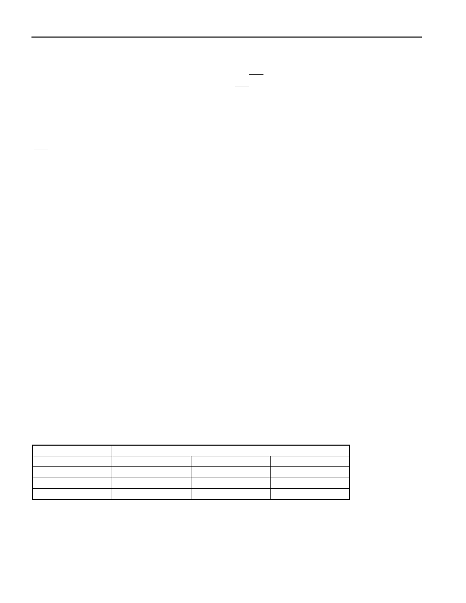
BLOCK DIAGRAM Figure 1
RST
3 3V
V
CC
TOLERANCE
BIAS
IN
2.5V
+
-
TIME
DELAY
1.25V T.C.
REFERENC
E
TOL
2.5V
GROUN
V
CC
TOLERANCE
BIAS
IN
3.3V
TOL
3.3V
TIME
DELAY
Level Sense
&
Debounce
MPBRS
+
-
100 k
TD
2.5V
TD
3.3V
100 k
PBRST
3.3V
PBRST
2.5V
100 k
+
-
+
-
IN
IN
NMI
NMI
RST
2.5V
DS1831C/D/E
3 of 14
OPERATION � POWER MONITOR
The DS1831 provides the functions of detecting out-of-tolerance conditions on a 3.3 (or 3) volt and
2.5 volt power supply and warning a processor based system of impending power failure. When an input
is detected as out-of-tolerance on either voltage input the
RST
for that supply will be forced active low.
When that input returns to a valid state the associated
RST
will remain active for the time delay selected
with the associated TD input and then return to an inactive state until the next input out-of-tolerance
condition.
On power-up both resets are kept active for the selected reset time after the associated power supply input
has reached the selected tolerance. This allows the power supply and system power to stabilize before
RST
is released.
All internal operating current for the DS1831 will be supplied by either the IN
3.3V
or IN
2.5V
input which
ever has the highest voltage level.
OPERATION - TOLERANCE SELECT
The DS1831 provides 2 TOL inputs for individual customization of the DS1831 to specific application
requirements. If the TOL for the 2.5 volt supply is tied to the 2.5 volt input a 5% tolerance is selected. If
the TOL is connected to ground a 10% tolerance is selected or if it is left unconnected a 15% tolerance is
selected. If the TOL for the 3.3 volt supply is tied to the 3.3 volt input a 5% tolerance is selected, a 10%
tolerance is selected if it is connected to ground, and a 20% tolerance is selected if the input is left
unconnected. These tolerance conditions are set at power up and can only be changed by power cycling
the device.
OPERATION - RESET TIME-DELAY SELECT
The DS1831 provides 2 TD inputs for individual customization of reset time delays and an additional one
for the DS1831D watchdog. TD inputs select time delays for the IN
2.5V
and IN
3.3V
resets outputs and the
Watchdog on the DS1831D. The reset time delays are shown in table 1. These allow the selection of
minimum delays of 10 ms, 100 ms, and 1000 ms.
Wiring an individual reset output to the push-button input of the other voltage reset allows custom reset
timings or allows for the sequencing of the reset outputs. See figure 2.
These time delays are set at power-up and cannot be changed after the device reaches an in-tolerance
condition.
TD INPUTS/RESET AND WATCHDOG TIME-DELAYS Table 1
RESET TIME-DELAY
TD
MIN
TYP
MAX
GND
10 ms
16 ms
20 ms
Float
100 ms
160 ms
200 ms
V
CC
1000 ms
1600 ms
2000 ms
DS1831C/D/E
4 of 14
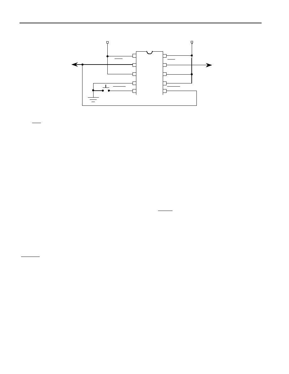
PUSHBUTTON RESET SEQUENCING Figure 2
*NOTE:
The
RST
2.5
volt output is connected to the IN
3.3V
via a 100 k
resistor in the push-button input and
therefore does not require a pull-up resistor (an addition pull up can be used to accelerate responses.) If
an external pull-up is used in this example it must be connected to the 3.3 volt power supply.
OPERATION - PUSHBUTTON RESET
The DS1831 provides 3 pushbutton inputs for manual reset of the device. Pushbutton inputs for the
3.3 volt reset, 2.5 volt reset, and a master pushbutton reset (DS1831C & DS1831D only) input; provide
multiple options for system control. The 3.3 volt pushbutton reset and 2.5 volt pushbutton resets provide
a simple manual reset for the associated reset output; while the master pushbutton reset forces all resets
and NMI outputs active low.
The 2.5 volt reset pushbutton input and the 3.3 volt reset pushbutton input provide manual reset control
for each associated reset output. When the output associated with a pushbutton input is not active, a
pushbutton reset can be generated by pulling the associated
PBRST
pin low for at least 20 �s. When the
pushbutton is held low the reset will be forced active and will remain active for a reset cycle after the
pushbutton is released. See figure 2 for an application example that allows a user to sequence the reset
outputs.
A master pushbutton reset cycle can be started if at least one voltage input (IN
2.5V
, IN
3.3V
, IN1, or IN2) is
in tolerance and at least 1 output is active. A master pushbutton reset is generated by pulling the
MPBRST
pin low for at least 20 �s. When the pushbutton is held low all outputs are forced active and
will remain active for a reset or NMI time delay after the pushbutton is released. The Master Pushbutton
input is pulled high through an internal 100 k
pull up resistor and debounced via internal circuitry. See
figure 3 for an application example. Figures 4 and 5 for the timing diagram.
The 2.5 volt and 3.3 volt pushbutton reset inputs are pulled high through an internal 100 k
pull up
resistor to the voltage input, which is associated with that pushbutton. The master pushbutton is pulled to
the greater of the "IN
2.5V
" and "IN
3.3V
" inputs.
*Caution should be exercised to avoid pulling the pushbutton inputs above associated supply inputs.
Generally all pushbutton inputs should be driven low with open drain inputs.
RST
2.5V
PBRST
3.3V
GND
TD
2.5V
IN
3.3V
IN
2.5V
RST
3.3V
TOL
3.3V
PBRST
2.5V
TOL
2.5V
DS1831C
TD
3.3V
2.5V Supply
3.3V Supply
1
2
3
4
5
16
15
14
13
12
*
DS1831C/D/E
5 of 14
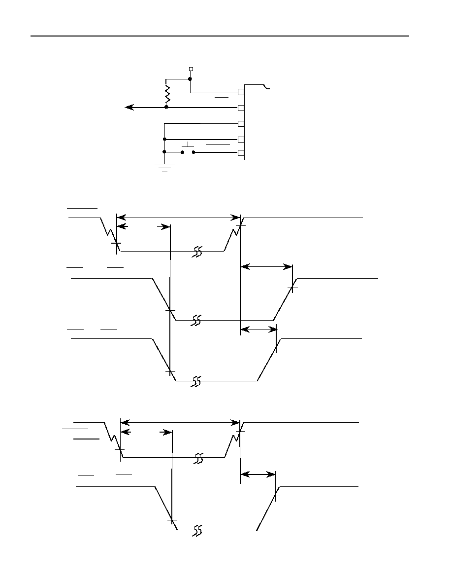
PUSHBUTTON RESET Figure 3
TIMING DIAGRAM � MASTER PUSHBUTTON RESET Figure 4
TIMING DIAGRAM � 2.5V OR 3.3V PUSHBUTTON RESET Figure 5
RST
2.5V
GND
TD
2.5V
IN
2.5V
PBRST
2.5V
TOL
2.5V
2.5V Supply
1
2
3
4
5
16
15
14
13
12
DS1831C
10 k
V
IH
V
IL
t
PDLY
t
PB
t
RST
MPBRST
RST
2.5V
and RST
3.3V
V
OH
t
NMI
NMI1 and NMI2
V
OH
V
IH
V
IL
t
PDLY
t
PB
t
RST
PBRST
2.5V
(or PBRST
3.3V
)
RST
2.5V
(or RST
3.3V
)
V
OH
V
IL