 | –≠–ª–µ–∫—Ç—Ä–æ–Ω–Ω—ã–π –∫–æ–º–ø–æ–Ω–µ–Ω—Ç: DS2143Q | –°–∫–∞—á–∞—Ç—å:  PDF PDF  ZIP ZIP |

1 of 44
112099
FEATURES
E1/ISDN-PRI framing transceiver
Frames to CAS, CCS, and CRC4 formats
Parallel control port
Onboard two frame elastic store slip buffer
Extracts and inserts CAS signaling bits
Programmable output clocks for fractional E1
links, DS0 loopbacks, and drop and insert
applications
Onboard Sa data link support circuitry
FEBE E-Bit detection, counting and
generation
Pin-compatible with DS2141A T1 Controller
5V supply; low power (50 mW) CMOS
Available in 40-pin DIP and 44-pin PLCC
(DS2143Q)
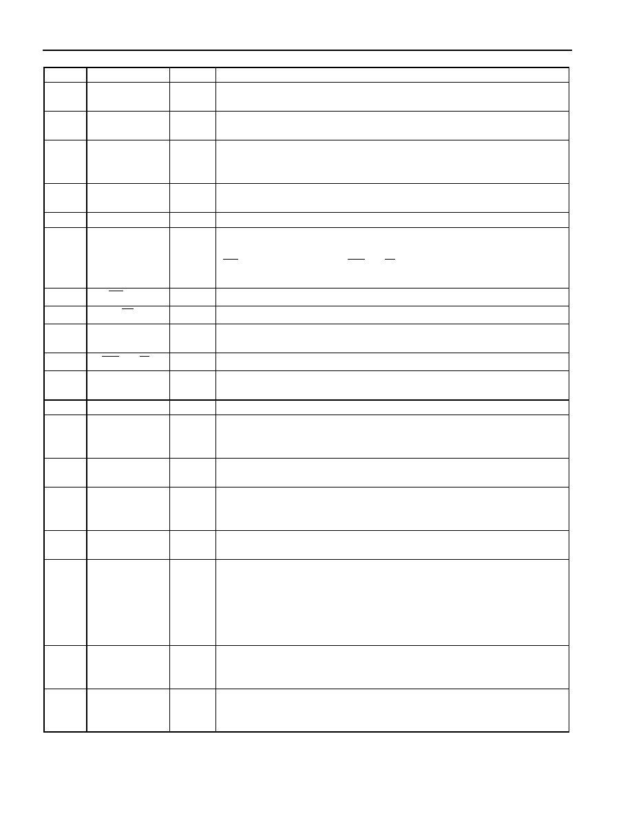
PIN ASSIGNMENT
DESCRIPTION
The DS2143 is a comprehensive, software-driven E1 framer. It is meant to act as a slave or coprocessor to
a microcontroller or microprocessor. Quick access via the parallel control port allows a single micro to
handle many E1 lines. The DS2143 is very flexible and can be configured into numerous orientations via
software. The software orientation of the device allows the user to modify their design to conform to
future E1 specification changes. The controller contains a set of 69 8-bit internal registers which the user
DS2143/DS2143Q
E1 Controller
www.dalsemi.com
40-Pin DIP (600-mil)
13
39
TCHCLK
TNEG
AD1
AD2
AD3
AD4
AD5
AD6
BTS
AD7
VDD
TLCLK
INT1
INT2
RLOS/LOTC
TCHBLK
RCHBLK
LI_CS
LI_CLK
LI_SDI
RNEG
SYSCLK
1
2
3
4
5
6
7
8
9
10
11
12
14
40
38
37
36
35
34
33
32
31
30
29
27
28
TSER
TPOS
AD0
TCLK
TSYNC
TLINK
19
RD(DS)
CS
ALE(AS)
WR(R/W)
VSS
RLINK
RPOS
RSYNC
RSER
RCHCLK
RLCLK
RCLK
15
16
17
18
20
26
25
24
23
21
22
IN
T2
AD0
AD1
AD2
AD3
AD4
AD5
RLOS/LOTC
TCHBLK
RCHBLK
LI_CS
LI_CLK
LI_SDI
AD6
NC
TN
EG
TPOS T
CHCLK
TSER TC
LK
VD
D
TSYN
C
NC CS
AL
E(
A
S
)
WR(R/
W
)
RLI
N
K
VS
S
RLCL
K
39
38
37
36
35
34
33
7
8
9
10
11
12
13
6 5 4 3 2 1 44 43 42 41 40
18 19 20 21 22 23 24 25 26 27 28
AD7
BTS
RD(DS)
NC
TLIN
K
TLC
L
K
IN
T1
RCL
K
RCHCL
K
RS
E
R
RS
Y
N
C
14
15
16
17
NC
SYSCLK
RNEG
RPOS
32
31
30
29
44-PIN PLCC

DS2143/DS2143Q
2 of 44
can access. These internal registers are used to configure the device and obtain information from the E1
link. The device fully meets al l of the latest E1 specifications, including CCITT G.704, G.706, and
G.732.
1.0 INTRODUCTION
The DS2143 E1 Controller has four main sections: the receive side, the transmit side, the line interface
controller, and the parallel control port. See the Block Diagram. On the receive side, the device will
clock in the serial E1 stream via the RPOS and RNEG pins. The synchronizer will locate the frame and
multiframe patterns and establish their respective positions. This information will be used by the rest of
the receive side circuitry.
The DS2143 is an "off-line" framer, which means that all of the E1 serial stream that goes into the device
will come out of it unchanged. Once the E1 data has been framed to, the signaling data can be extracted.
The two-frame elastic store can either be enabled or bypassed.
The transmit side clocks in the unframed E1 stream at TSER and add in the framing pattern and the
signaling. The line interface control port will update line interface devices that contain a serial port. The
parallel control port contains a multiplexed address and data structure which can be connected to either a
microcontroller or microprocessor.
Reader's Note:
This data sheet assumes a particular nomenclature of the E1 operating environment. There are 32 8-bit
timeslots in an E1 systems which are number 0 to 31. Timeslot 0 is transmitted first and received first.
These 32 timeslots are also referred to as channels with a numbering scheme of 1 to 32. Timeslot 0 is
identical to channel 1, timeslot 1 is identical to channel 2, and so on. Each timeslot (or channel) is made
up of 8 bits which are numbered 1 to 8. Bit number 1 is the MSB and is transmitted first. Bit number 8 is
the LSB and is transmitted last. Throughout this data sheet, the following abbreviations will be used:
FAS Frame
Alignment
Signal
CRC4
Cyclical Redundancy Check
CAS
Channel Associated Signaling
CCS
Common Channel Signaling
MF Multiframe
Sa Additional
bits
Si International
bits
E-bit
CRC4 Error Bits

DS2143/DS2143Q
3 of 44
DS2143 FEATURES
Parallel control port
Onboard two-frame elastic store
CAS signaling bit extraction and insertion
Fully independent transmit and receive sections
Full alarm detection
Full access to Si and Sa bits
Loss of transmit clock detection
HDB3 coder/decoder
Full transmit transparency
Large error counters
Individual bit-by-bit Sa data link support circuitry
Programmable output clocks
Frame sync generation
Local loopback capability
Automatic CRC4 E-bit support
Loss of receive clock detection
G.802 E1 to T1 mapping support
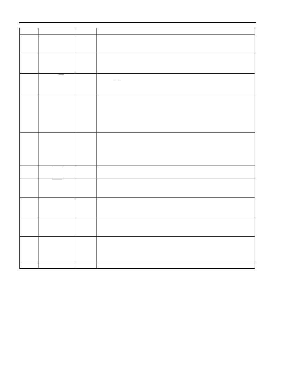
DS2143 BLOCK DIAGRAM
DS2143/DS2143Q
4 of 44
PIN DESCRIPTION Table 1
PIN
SYMBOL
TYPE
DESCRIPTION
1
TCLK
I
Transmit Clock. 2.048 MHz primary clock. A clock must be
applied at the TCLK pin for the parallel port to operate properly.
2
TSER
I
Transmit Serial Data. Transmit NRZ serial data, sampled on the
falling edge of TCLK.
3
TCHCLK
O
Transmit Channel Clock. 256 kHz clock which pulses high during
the LSB of each channel. Useful for parallel-to-serial conversion of
channel data. See Section 13 for timing details.
4
5
TPOS
TNEG
O
Transmit Bipolar Data. Updated on rising edge of TCLK. For
optical links, can be programmed to output NRZ data.
6-13
AD0-AD7
I/O
Address/Data Bus. An 8-bit multiplexed address/data bus.
14
BTS
I
Bus Type Select. Strap high to select Motorola bus timing; strap
low to select Intel bus timing. This pin controls the function of
RD
(DS), ALE(AS), and
WR
(R/
W
) pins. If BTS=1, then these pins
assume the function listed in parentheses ().
15
RD
(DS)
I
Read Input (Data Strobe).
16
CS
I
Chip Select. Must be low to read or write the port.
17
ALE(AS)
I
Address Latch Enable (Address Strobe). A positive-going edge
serves to demultiplex the bus.
18
WR
(R/
W
)
I
Write Input (Read/Write).
19
RLINK
O
Receive Link Data. Outputs Sa bits. See Section 13 for timing
details.
20
V
SS
-
Signal Ground. 0.0 volts.
21
RLCLK
O
Receive Link Clock. 4 kHz to 20 kHz demand clock for the
RLINK output. Controlled by RCR2. See Section 13 for timing
details.
22
RCLK
I
Receive Clock. 2.048 MHz primary clock. A clock must be applied
at the RCLK pin for the parallel port to operate properly.
23
RCHCLK
O
Receive Channel Clock. 256 kHz clock which pulses high during
the LSB of each channel. Useful for serial to parallel conversion of
channel data. See Section 13 for timing details.
24
RSER
O
Receive Serial Data. Received NRZ serial data, updated on rising
edges of RCLK.
25
RSYNC
I/O
Receive Sync. An extracted pulse, one RCLK wide, is output at this
pin which identifies either frame (RCR1.6=0) or multiframe
boundaries (RCR1.6=1). If the elastic store is enabled via the
RCR2.1, then this pin can be enabled to be an input via RCR1.5 at
which a frame boundary pulse is applied. See Section 13 for timing
details.
26
27
RPOS
RNEG
I
Receive Bipolar Data Inputs. Sampled on falling edge of RCLK.
Tie together to receive NRZ data and disable BPV monitoring
circuitry.
28
SYSCLK
I
System Clock. 1.544 MHz or 2.048 MHz clock. Only used when
the elastic store function is enabled via the RCR2.1. Should be tied
low in applications that do not use the elastic store.
DS2143/DS2143Q
5 of 44
PIN
SYMBOL
TYPE
DESCRIPTION
29
LI_SDI
O
Serial Port Data for the Line Interface. Connects directly to the
SDI input pin on the line interface. See Sections 12 and 13 for
timing details.
30
LI_CLK
O
Serial Port Clock for the Line Interface. Connects directly to the
SCLK input pin on the line interface. See Sections 12 and 13 for
timing details.
31
LI_
CS
O
Serial Port Chip Select for the Line Interface. Connects directly
to the
CS
input pin on the line interface. See Sections 12 and 13 for
timing details.
32
33
RCHBLK
TCHBLK
O
Receive/Transmit Channel Block. A user programmable output
that can be forced high or low during any of the 32 E1 channels.
Useful for blocking clocks to a serial UART or LAPD controller in
applications where not all E1 channels are used such as Fractional
E1 or ISDN-PRI. Also useful for locating individual channels in
drop-and-insert applications. See Sections 9 and 13 for details.
34
RLOS/LOTC
O
Receive Loss of Sync/Loss of Transmit Clock. A dual function
output. If TCR2.0=0, then this pin will toggle high when the
synchronizer is searching for the E1 frame and multiframe. If
TCR2.0=1, then this pin will toggle high if the TCLK pin has not
toggled for 5
µ
s.
35
INT2
O
Receive Alarm Interrupt 2. Flags host controller during conditions
defined in Status Register 2. Active low, open drain output.
36
INT1
O
Receive Alarm Interrupt 1. Flags host controller during alarm
conditions defined in Status Register 1. Active low, open drain
output.
37
TLCLK
O
Transmit Link Clock. 4 kHz to 20 kHz demand clock for the
TLINK input. Controlled by TCR2. See Section 13 for timing
details.
38
TLINK
I
Transmit Link Data. If enabled, this pin will be sampled on the
falling edge of TCLK to insert Sa bits. See Section 13 for timing
details.
39
TSYNC
I/O
Transmit Sync. A pulse at this pin will establish either frame or
CAS multiframe boundaries for the DS2143. Via TCR1.1, the
DS2143 can be programmed to output either a frame or multiframe
pulse at this pin. See Section 13 for timing details.
40
VDD
-
Positive Supply. 5.0 volts.