 | –≠–ª–µ–∫—Ç—Ä–æ–Ω–Ω—ã–π –∫–æ–º–ø–æ–Ω–µ–Ω—Ç: DS2175N | –°–∫–∞—á–∞—Ç—å:  PDF PDF  ZIP ZIP |

1 of 12
092099
FEATURES
∑
Rate buffer for T1 and CEPT transmission
systems
∑
Synchronizes loop≠timed and system timed
data streams on frame boundaries
∑
Ideal for T1 (1.544 MHz) to CEPT (2.048
MHz), CEPT to T1 interfaces
∑
Supports parallel and serial backplanes
∑
Buffer depth is 2 frames
∑
Comprehensive on≠chip "slip" control logic
≠ Slips occur only on frame boundaries
≠ Outputs report slip occurrences and
direction
≠ Align feature allows buffer to be recentered
at any time
≠ Buffer depth easily monitored
∑
Compatible with DS2180A T1 and DS2181A
CEPT Transceivers
∑
Industrial temperature range of ≠40
∞
C to
+85
∞
C available, designated DS2175N
PIN ASSIGNMENT
DESCRIPTION
The DS2175 is a low≠power CMOS elastic≠store memory optimized for use in primary rate telecommu-
nications transmission equipment. The device serves as a synchronizing element between async data
streams and is compatible with North American (T1≠1.544 MHz) and European (CEPT≠2.048 MHz) rate
networks. The chip has several flexible operating modes which eliminate support logic and hardware cur-
rently required to interconnect parallel or serial TDM backplanes. Application areas include digital
trunks, drop and insert equipment, digital cross≠connects (DACS), private network equipment and
PABX≠to≠computer interfaces such as DMI and CPI.
DS2175
T1/CEPT Elastic Store
www.dalsemi.com
16-PIN DIP (300 MIL)
16-PIN SOIC (300 MIL)
1
2
3
4
5
6
7
8
16
15
14
13
12
11
10
9
VDD
SYSCLK
SFSYNC
SSER
SCHCLK
S/P
SCLKSEL
RCLKSEL
RCLK
RSER
RMSYNC
FSD
SLIP
VSS
ALN
SMSYNC

DS2175
2 of 12
DS2175 BLOCK DIAGRAM Figure 1
DS2175
3 of 12
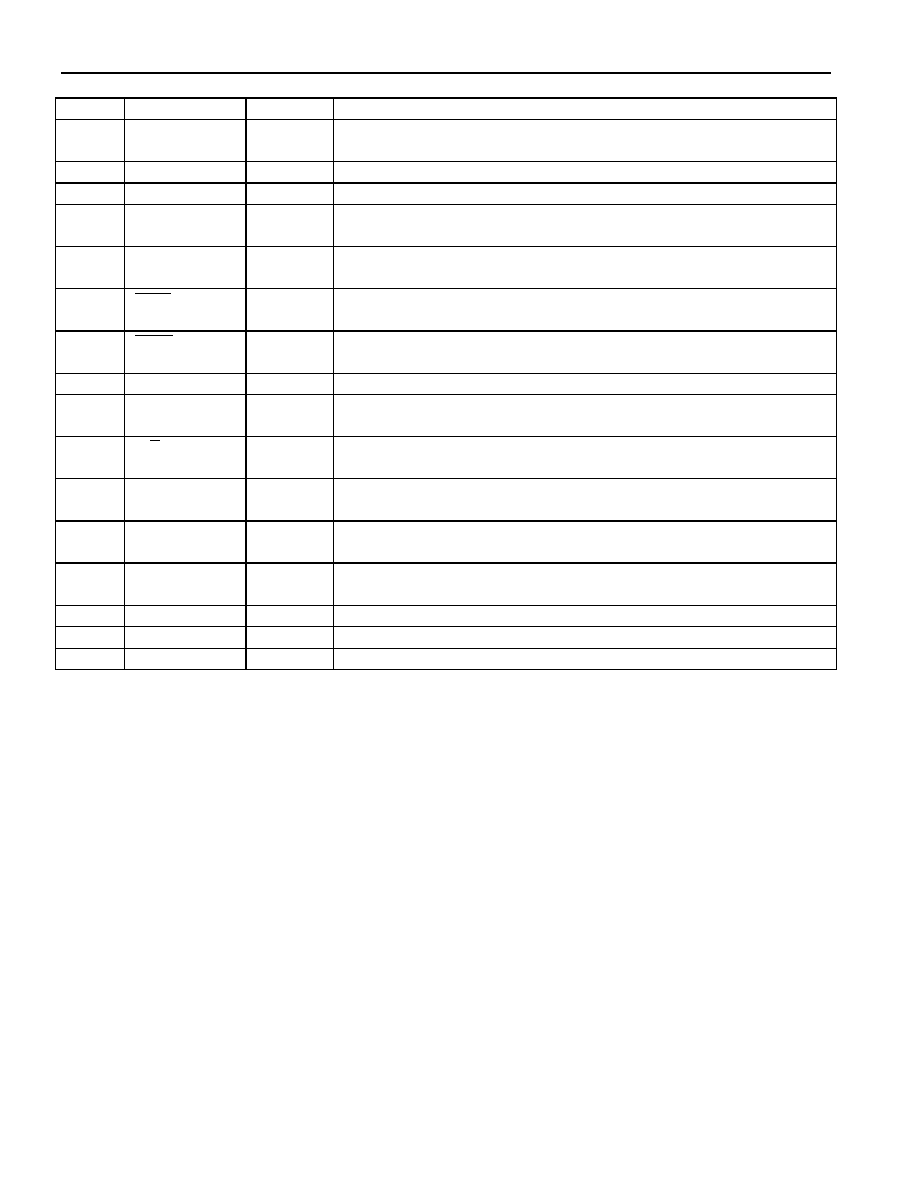
PIN Description Table 1
PIN
SYMBOL
TYPE
DESCRIPTION
1
RCLKSEL
I
Receive Clock Select. Tie to V
SS
for 1.544 MHz applications, to
V
DD
for 2.048 MHz.
2
RCLK
I
Receive Clock. 1.544 or 2.048 MHz data clock.
3
RSER
I
Receive Serial Data. Sampled on falling edge of RCLK.
4
RMSYNC
I
Receive Multifram Sync. Rising edge establishes receive side
frame and multiframe boundaries.
5
FSD
O
Frame Slip Directions. State indicates direction of last slip;
latched on slip occurrence.
6
SLIP
O
Frame Slip. Active low, open collector output. Held low for 65
SYSCLK cycles when a slip occurs.
7
ALN
I
Align. Recenters buffer on next system side frame boundary when
forced low; negative edge-triggered.
8
V
SS
≠
Signal Ground. 0.0 volts.
9
SCLKSEL
I
System Clock Select. Tie to V
SS
for 1.544 MHz applications, to
V
DD
for 2.048 MHz.
10
S/
P
I
Serial/Parallel Select. Tie to V
SS
for parallel backplane
applications, to V
DD
for serial.
11
SCHCLK
O
System Channel Clock. Transitions high on channel boundaries;
useful for serial to parallel conversion of channel data.
12
SFSYNC
I
System Frame Sync. Rising edge establishes system side frame
boundaries.
13
SMSYNC
O
System Multiframe Sync. Slip-compensated multiframe output;
used with RMSYNC to monitor depth of store real time.
14
SSER
O
System Serial Data. Updated on rising edge of SYSCLK.
15
SYSCLK
I
System Clock. 1.544 or 2.048 MHz data clock.
16
V
DD
≠
Positive Supply. 5.0 volts.
PCM BUFFER
The DS2175 utilizes a 2≠frame buffer to synchronize in-coming PCM data to the system backplane clock.
Buffer depth is mode≠dependent; 2.048 MHz to 2.048 MHz applications utilize 64 bytes of buffer
memory, while all other modes are supported by 48 bytes. The buffer samples data at RSER on the falling
edge of RCLK. Output data appears at SSER and is updated on the rising edge of SYSCLK. The buffer
depth is constantly monitored by onboard contention logic; a "slip" occurs when the buffer is completely
emptied or filled. Slips automatically recenter the buffer to a one≠frame depth and always occur on frame
boundaries.
DATA FORMAT
Data is presented to, and output from, the elastic store in a "framed" format. A rising edge at RMSYNC
and SFSYNC establishes frame boundaries for the receive and system sides. North American (T1) frames
contain 24 data channels of 8 bits each and an F≠bit (193 bits total). European (CEPT) frames contain 32
data channels (256 bits). The frame rate of both systems is 8 KHz. RMSYNC and SFSYNC do not
require a pulse at every frame boundary; if desired, they may be pulsed once to establish frame alignment.
Internal counters will then maintain the frame alignment and may be reinforced by the next rising edge at
RMSYNC and/or SFSYNC.

DS2175
4 of 12
SLIP CORRECTION CAPABILITY
The 2≠frame buffer depth is adequate for T≠carrier and CEPT applications where short term jitter
synchronization, rather than correction of significant frequency differences, is required. The DS2175
provides an ideal balance between total delay (less than 250 microse-conds at its full depth) and slip
correction capability.
BUFFER RECENTERING
Many applications require that the buffer be recentered during system power≠up and/or initialization.
Forcing
ALN low recenters the buffer on the occurrence of the next frame sync boundary. A slip will
occur during this recentering if the buffer depth is adjusted. If the depth is presently optimum, no
adjustment (slip) occurs.
SLIP REPORTING
SLIP is held low for 65 SYSCLK cycles when a slip occurs. SLIP is an active≠low, open collector
output. FSD indicates slip direction. When low (buffer empty) a frame of data was "repeated" at SSER
during the previous slip. When high (buffer full), a frame of data was "deleted". FSD is updated at every
slip occurrence.
BUFFER DEPTH MONITORING
SMSYNC is a system side output pulse which indicates system side multiframe boundaries. The distance
between rising edges of RMSYNC and SMSYNC indicates the current buffer depth. Impending slip
conditions may be determined by monitoring RMSYNC and SMSYNC real time. SMSYNC is held high
for 65 SYSCLK periods.
CLOCK SELECT
Receive and system side clock frequencies are independently selectable by inputs RCLKSEL and
SCLKSEL. 1.544 MHz is selected when RCLKSEL (SCLKSEL) = 0; 2.048 MHz is selected when
RCLKSEL (SCLKSEL) = 1. In 1.544 MHz (receive) to 1.544 MHz (system) applications, the F-bit
position is passed through the receive buffer and presented at SSER immediately after the rising edge of
the system side frame sync. The F≠bit position is forced to 1 in 2.048 MHz to 1.544 MHz applications.
No F≠bit position exists in 2.048 MHz system side applications.
PARALLEL COMPATIBILITY
The DS2175 is compatible with parallel and serial backplanes. Channel 1 data appears at SSER after a
rising edge at SFSYNC (serial applications, S/
P
= 1). The device utilizes a look≠ahead circuit in parallel
applications (S/
P
= 0), and presents data 8 clocks early as shown in Figures 4 and 5. Converting SSER to
a parallel format requires an HC595 shift register.

DS2175
5 of 12
RECEIVE SIDE TIMING (RCLK = 1.544 MHz) Figure 2
RECEIVE SIDE TIMING (RCLK = 2.048 MHz) Figure 3
NOTES:
1.
All channel data is passed through the elastic store in 2.048 MHz system side applications
(SCLKSEL = 1);
2.
Data in channels >24 is ignored in 1.544 MHz system side applications (SCLKSEL = 0).
SYSTEM MULTIFRAME BOUNDARY TIMING (SYSCLK = 1.544 MHz) Figure 4
NOTES:
1.
In 1.544 MHz receive side applications (RCLKSEL=0), the F≠bit position contains F≠bit data
extracted from the data stream at RSER. The F≠bit position is forced to "1" in 2.048 MHz receive
side applications (RCLKSEL=1).
2.
In 2.048 MHz receive side applications (RCLKSEL=1), the E≠bit position is forced to "1" and data in
channels >24 is ignored.