 | –≠–ª–µ–∫—Ç—Ä–æ–Ω–Ω—ã–π –∫–æ–º–ø–æ–Ω–µ–Ω—Ç: DS2433T | –°–∫–∞—á–∞—Ç—å:  PDF PDF  ZIP ZIP |
1 of 19
062299
FEATURES
ß
4096 bits Electrically Erasable Programmable
Read Only Memory (EEPROM)
ß
Unique, factory-lasered and tested 64-bit
registration number (8-bit family code + 48-
bit serial number + 8-bit CRC tester) assures
absolute identity because no two parts are
alike
ß
Built-in multidrop controller ensures
compatibility with other MicroLAN products
ß
Memory partitioned into sixteen 256-bit pages
for packetizing data
ß
256-bit scratchpad with strict read/write
protocols ensures integrity of data transfer
ß
Reduces control, address, data and power to a
single data pin
ß
Directly connects to a single port pin of a
microprocessor and communicates at up to
16.3k bits per second
ß
Overdrive mode boosts communication speed
to 142k bits per second
ß
8-bit family code specifies DS2433
communication requirements to reader
ß
Presence detector acknowledges when reader
first applies voltage
ß
Low cost PR-35 or 8-pin SOIC surface mount
package
ß
Reads and writes over a wide voltage range of
2.8V to 6.0V from -40∞C to +85∞C
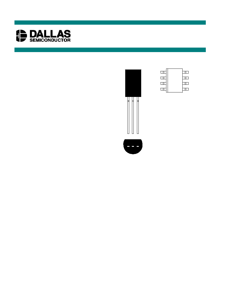
PIN ASSIGNMENT
PIN DESCRIPTION
PR-35
SOIC
Pin 1
Ground
NC
Pin 2
Data
NC
Pin 3
NC
Data
Pin 4
--
Ground
Pin 5-8
--
NC
ORDERING INFORMATION
DS2433
PR-35 package
DS2433S
8-pin SOIC package
DS2433T
Tape & Reel version of DS2433
DS2433Y
Tape & Reel version of DS2433S
DS2433X
Chip Scale Pkg., Tape & Reel
SILICON LABEL DESCRIPTION
The DS2433 4K-bit 1-Wire EEPROM identifies and stores relevant information about the product to
which it is associated. This lot or product specific information can be accessed with minimal interface,
for example a single port pin of a microcontroller. The DS2433 consists of a factory-lasered registration
number that includes a unique 48-bit serial number, an 8-bit CRC, and an 8-bit Family Code (23h) plus
4096 bits of user-programmable EEPROM. The power to read and write the DS2433 is derived entirely
DS2433
4k-Bit 1-Wire
TM
EEPROM
PRELIMINARY
www.dalsemi.com
NC
NC
DATA
GND
NC
2
3
4
8
7
6
5
1
8-PIN SOIC (208 MIL)
NC
NC
NC
1 2 3
3
2
1
PR-35
BOTTOM VIEW
DS2433
2 of 19
from the 1-Wire communication line. The memory is organized as sixteen pages of 256 bits each. The
scratchpad is an additional page that acts as a buffer when writing to memory. Data is first written to the
scratchpad where it may be read back for verification. A copy scratchpad command will then transfer the
data to memory. This process insures data integrity when modifying the memory. The 64-bit registration
number provides a guaranteed unique identity which allows for absolute traceability and acts as node
address if multiple DS2433 are connected in parallel to form a local network. Data is transferred serially
via the 1-Wire protocol which requires only a single data lead and a ground return. The PR-35 and SOIC
packages provide a compact enclosure that allows standard assembly equipment to handle the device
easily for attachment to printed circuit boards or wiring. Typical applications include storage of
calibration constants, board identification and product revision status.
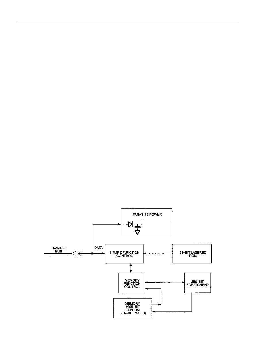
OVERVIEW
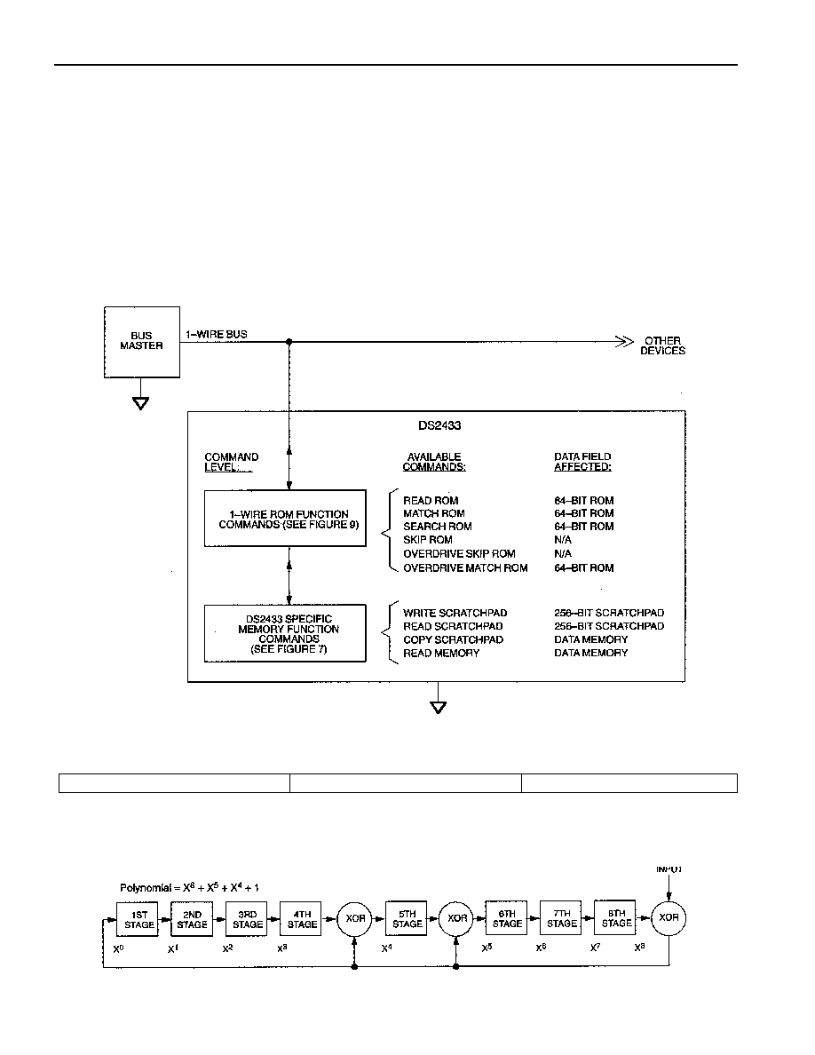
The block diagram in Figure 1 shows the relationships between the major control and memory sections of
the DS2433. The DS2433 has three main data components: 1) 64-bit lasered ROM, 2) 256-bit
scratchpad, and 3) 4096-bit EEPROM. The hierarchical structure of the 1-Wire protocol is shown in
Figure 2. The bus master must first provide one of the six ROM Function Commands, 1) Read ROM, 2)
Match ROM, 3) Search ROM, 4) Skip ROM, 5) Overdrive-Skip ROM or 6) Overdrive-Match ROM.
Upon completion of an overdrive ROM command byte executed at standard speed, the device will enter
Overdrive mode where all subsequent communication occurs at a higher speed. The protocol required for
these ROM function commands is described in Figure 9. After a ROM function command is successfully
executed, the memory functions become accessible and the master may provide any one of the four
memory function commands. The protocol for these memory function commands is described in Figure
7. All data is read and written least significant bit first.
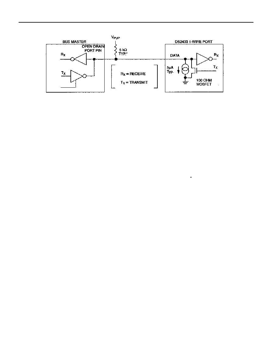
PARASITE POWER
The block diagram (Figure 1) shows the parasite-powered circuitry. This circuitry "steals" power
whenever the I/O input is high. I/O will provide sufficient power as long as the specified timing and
voltage requirements are met.
DS2433 BLOCK DIAGRAM Figure 1

DS2433
3 of 19
64-BIT LASERED ROM
Each DS2433 contains a unique ROM code that is 64 bits long. The first eight bits are a 1-Wire family
code. The next 48 bits are a unique serial number. The last eight bits are a CRC of the first 56 bits. (See
Figure 3.) The 1-Wire CRC is generated using a polynomial generator consisting of a shift register and
XOR gates as shown in Figure 4. The polynomial is X
8
+ X
5
+ X
4
+ 1. Additional information about the
Dallas 1-Wire Cyclic Redundancy Check is available in the Book of DS19xx iButton Standards.
The shift register bits are initialized to zero. Then starting with the least significant bit of the family code,
one bit at a time is shifted in. After the 8
th
bit of the family code has been entered, then the serial number
is entered. After the 48
th
bit of the serial number has been entered, the shift register contains the CRC
value. Shifting in the eight bits of CRC should return the shift register to all zeros.
MEMORY
The memory map in Figure 5 shows a 32-byte page called the scratchpad and additional 32-byte pages
called memory. The DS2433 contains pages 0 through 15 which make up the 4096-bit EEPROM. The
scratch-pad is an additional page that acts as a buffer when writing to memory.
ADDRESS REGISTERS AND TRANSFER STATUS
Because of the serial data transfer, the DS2433 employs three address registers, called TA1, TA2 and E/S
(Figure 6). Registers TA1 and TA2 must be loaded with the target address to which the data will be
written or from which data will be sent to the master upon a Read command. Register E/S acts like a byte
counter and Transfer Status register. It is used to verify data integrity with write commands. Therefore,
the master only has read access to this register. The lower five bits of the E/S register indicate the address
of the last byte that has been written to the scratchpad. This address is called Ending Offset. Bit 5 of the
E/S register, called PF, is set if the number of data bits sent by the master is not an integer multiple of 8 or
if the data in the scratchpad is not valid due to a loss of power. A valid write to the scratchpad will clear
the PF bit. Bit 6 has no function; it always reads 0. Note that the lowest five bits of the target address
also determine the address within the scratchpad, where intermediate storage of data will begin. This
address is called byte offset. If the target address (TA1) for a Write command is 03CH for example, then
the scratchpad will store incoming data beginning at the byte offset 1CH and will be full after only four
bytes. The corresponding ending offset in this example is 1FH. For best economy of speed and
efficiency, the target address for writing should point to the beginning of a new page, i.e., the byte offset
will be 0. Thus the full 32-byte capacity of the scratchpad is available, resulting also in the ending offset
of 1FH. However, it is possible to write one or several contiguous bytes somewhere within a page. The
ending offset together with the Partial Flag support the master checking the data integrity after a Write
command. The highest valued bit of the E/S register, called AA is valid only if the PF flag reads 0. If PF
is 0 and AA is 1, a copy has taken place. The AA bit is cleared when the device receives a write
scratchpad command.
WRITING WITH VERIFICATION
To write data to the DS2433, the scratchpad has to be used as intermediate storage. First the master
issues the Write Scratchpad command to specify the desired target address, followed by the data to be
written to the scratchpad. Under certain conditions (see Write Scratchpad command) the master will
receive an inverted CRC16 of the command, address and data at the end of the write scratchpad command
sequence. Knowing this CRC value, the master can compare it to the value it has calculated itself to
decide if the communication was successful and proceed to the Copy Scratchpad command. If the master
could not receive the CRC16, it has to send the Read Scratchpad command to read back the scratchpad to
verify data integrity. As preamble to the scratchpad data, the DS2433 repeats the target address TA1 and
TA2 and sends the contents of the E/S register. If the PF flag is set, data did not arrive correctly in the
DS2433
4 of 19
scratchpad or there was a loss of power since data was last written to the scratchpad. The master does not
need to continue reading; it can start a new trial to write data to the scratchpad. Similarly, a set AA flag
together with a cleared PF flag indicates that the Write command was not recognized by the device. If
everything went correctly, both flags are cleared and the ending offset indicates the address of the last
byte written to the scratchpad. Now the master can continue reading and verifying every data byte.
After the master has verified the data, it has to send the Copy Scratchpad command. This command must
be followed exactly by the data of the three address registers TA1, TA2 and E/S. The master may obtain
the contents of these registers by reading the scratchpad or derive it from the target address and the
amount of data to be written. As soon as the DS2433 has received these bytes correctly, it will copy the
data to the requested location beginning at the target address.
HIERARCHCAL STRUCTURE FOR 1-WIRE PROTOCOL Figure 2
64-BIT LASERED ROM Figure 3
MSB
LSB
8-Bit CRC Code
48-Bit Serial Number
8-Bit Family Code (23h)
MSB
LSB MSB
LSB MSB
LSB
1-WIRE CRC GENERATOR Figure 4
INPUT

DS2433
5 of 19
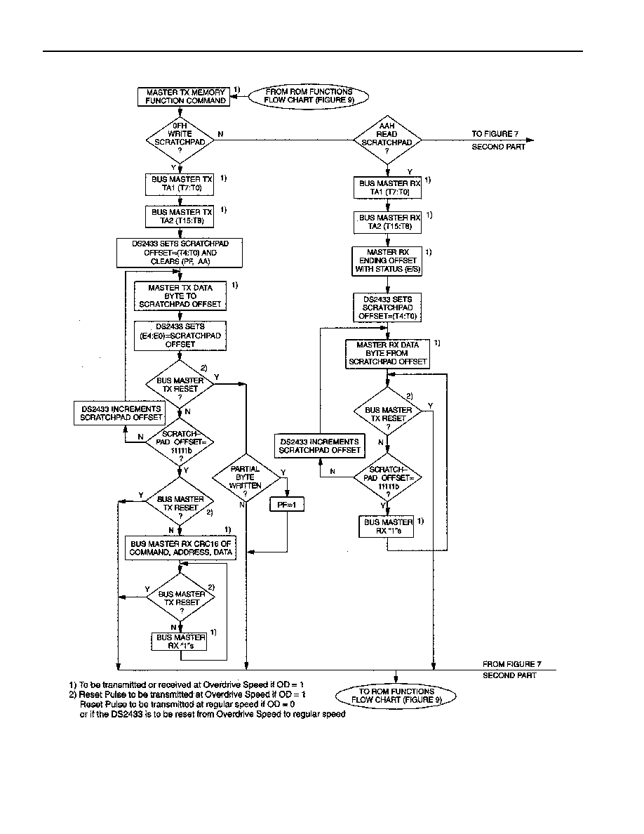
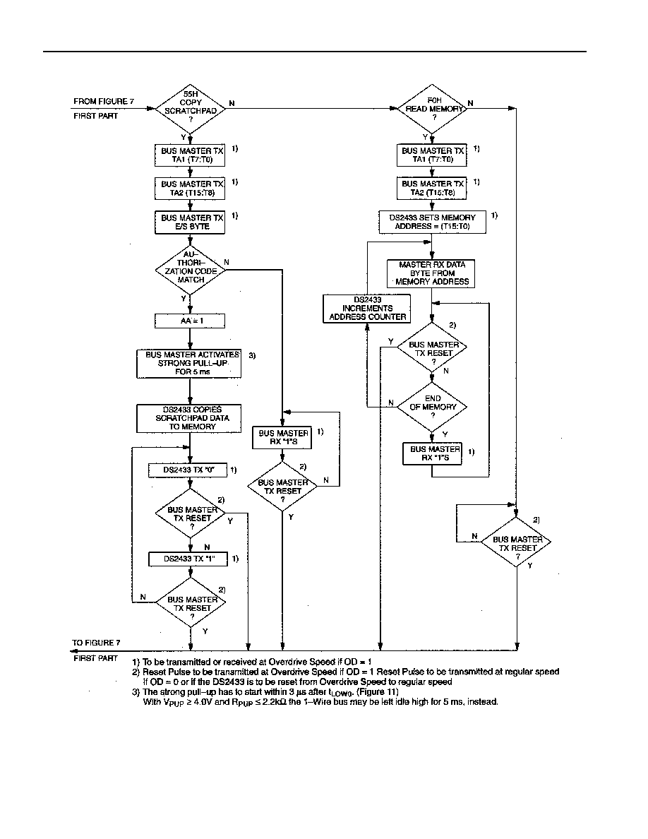
MEMORY FUNCTION COMMANDS
The "Memory Function Flow Chart" (Figure 7) describes the protocols necessary for accessing the
memory. An example follows the flowchart. The communication between master and DS2433 takes
place either at regular speed (default, OD = 0) or at Overdrive Speed (OD = 1). If not explicitly set into
the Overdrive Mode the DS2433 assumes regular speed.
WRITE SCRATCHPAD COMMAND [0FH]
After issuing the write scratchpad command, the master must first provide the 2-byte target address,
followed by the data to be written to the scratchpad. The data will be written to the scratchpad starting at
the byte offset (T4:T0). The ending offset (E4:E0) will be the byte offset at which the master stops
writing data. Only full data bytes are accepted. If the last data byte is incomplete its content will be
ignored and the partial byte flag PF will be set.
When executing the Write Scratchpad command the CRC generator inside the DS2433 (see Figure 12)
calculates a CRC over the entire data stream, starting at the command code and ending at the last data
byte sent by the master. This CRC is generated using the CRC16 polynomial by first clearing the CRC
generator and then shifting in the command code (0FH) of the Write Scratchpad command, the Target
Addresses TA1 and TA2 as supplied by the master and all the data bytes. The master may end the Write
Scratchpad command at any time. However, if the ending offset is 11111b, the master may send 16 read
time slots and will receive the CRC generated by the DS2433.
The memory address range of the DS2433 is 0000H to 01FFH. If the bus master sends a target address
higher than this, the internal circuitry of the chip will set the seven most significant address bits to zero as
they are shifted into the internal address register. The Read Scratchpad command will reveal the target
address as it will be used by the DS2433. The master will identify such address modifications by
comparing the target address read back to the target address transmitted. If the master does not read the
scratchpad, a subsequent copy scratchpad command will not work since the most significant bits of the
target address the master sends will not match the value the DS2433 expects.
READ SCRATCHPAD COMMAND [AAH]
This command is used to verify scratchpad data and target address. After issuing the read scratchpad
command, the master begins reading. The first two bytes will be the target address. The next byte will be
the ending offset/data status byte (E/S) followed by the scratchpad data beginning at the byte offset (T4:
T0). The master may read data until the end of the scratchpad after which the data read will be all logic
1's.
COPY SCRATCHPAD [55H]
This command is used to copy data from the scratchpad to memory. After issuing the copy scratchpad
command, the master must provide a 3-byte authorization pattern which can be obtained by reading the
scratchpad for verification. This pattern must exactly match the data contained in the three address
registers (TA1, TA2, E/S, in that order). If the pattern matches, the AA (Authorization Accepted) flag
will be set and the copy will begin. Copy takes 5 ms maximum during which the voltage on the 1-Wire
bus must not fall below 2.8V. A pattern of alternating 1s and 0s will be received after the data has been
copied until a Reset Pulse is issued by the master.
The data to be copied is determined by the three address registers. The scratchpad data from the
beginning offset through the ending offset, will be copied to memory, starting at the target address.
Anywhere from 1 to 32 bytes may be copied to memory with this command.
DS2433
6 of 19
DS2433 MEMORY MAP Figure 5
ADDRESS REGISTER Figure 6
READ MEMORY [F0H]
The read memory command may be used to read the entire memory. After issuing the command, the
master must provide the 2-byte target address. After the two bytes, the master reads data beginning from
the target address and may continue until the end of memory, at which point logic 1's will be read. It is
important to realize that the target address registers will contain the address provided. The ending
offset/data status byte is unaffected.
The hardware of the DS2433 provides a means to accomplish error-free writing to the memory section.
To safeguard reading data in the 1-Wire environment and to simultaneously speed up data transfers, it is
recommended to packetize data into data packets of the size of one memory page each. Such a packet
would typically store a 16-bit CRC with each page of data to insure rapid, error-free data transfers that
eliminate having to read a page multiple times to determine if the received data is correct or not. (See the
Book of DS19xx iButton Standards, Chapter 7 or Application Note 114 for the recommended file
structure.)
32-BIT INTERMEDIATE STORAGE SCRATCHPAD
32-BYTE FINAL STORAGE EEPROM
32-BYTE FINAL STORAGE EEPROM
FINAL STORAGE EEPROM
32-BYTE FINAL STORAGE EEPROM
ADDRESS
0000H TO
001FH
003FH
01DFH
01FFH
0020H TO
0040H TO
1FE0H TO
PAGE 0
PAGE 1
PAGE 2
TO PAGE 14
PAGE 15
T7
T6
T5
T4
T3
T2
T1
T0
T15
AA
1)
PF
E4
E3
E2
E1
E0
T14 T13 T12 T11 T10 T9
T8
TARGET ADDRESS (TA1)
TARGET ADDRESS (TA2)
ENDING ADDRESS WITH
DATA STATUS (E/S)
(READ ONLY)
1) THIS BIT WILL ALWAYS BE 0.
DS2433
7 of 19
MEMORY FUNCTION FLOW CHART Figure 7
DS2433
8 of 19
MEMORY FUNCTION FLOW CHART Figure 7 (continued)

DS2433
9 of 19
MEMORY FUNCTION EXAMPLE
Example: Write two data bytes to memory location 0026 and 0027. Read entire memory.
MASTER MODE
DATA (LSB FIRST)
COMMENTS
TX
Reset
Reset Pulse (480 - 960
µ
s)
RX
Presence
Presence Pulse
TX
CCH
Issue Skip ROM Command
TX
0FH
Issue Write Scratchpad command
TX
26H
TA1, beginning offset = 26H
TX
00H
TA2, address = 0026H
TX
<2 data bytes>
Write 2 bytes of data to scratchpad
TX
Reset
Reset Pulse
RX
Presence
Presence Pulse
TX
CCH
Issue Skip ROM Command
TX
AAH
Issue Read Scratchpad command
RX
26H
Read TA1, beginning offset = 26H
RX
00H
Read TA2, address = 0026H
RX
07H
Read E/S, ending offset = 7H, flags = 0H
RX
<2 data bytes>
Read scratchpad data and verify
TX
Reset
Reset Pulse
RX
Presence
Presence Pulse
TX
CCH
Issue Skip ROM Command
TX
55H
Issue Copy Scratchpad command
TX
26H
TX
00H
TX
07H
TA1
TA2
AUTHORIZATION CODE
E/S
TX
<idle or strong pullup>
Wait 5 ms
TX
Reset
Reset Pulse
RX
Presence
Presence Pulse
TX
CCH
Issue Skip ROM Command
TX
F0H
Issue Read Memory command
TX
00H
TA1, beginning offset = 0
TX
00H
TA2, address = 0000H
RX
<512 bytes>
Read entire memory
TX
Reset
Reset Pulse
RX
Presence
Presence Pulse, done
DS2433
10 of 19
HARDWARE CONFIGURATION Figure 8
*5k
is adequate for reading the DS2433. To write to a single device, a 2.2k
resistor and V
PUP
of at
least 4.0V is sufficient. For writing multiple DS2433s simultaneously or operation at low V
PUP
, the
resistor should be bypassed by a low-impedance pullup to V
PUP
while the device copies the scratchpad to
EEPROM.
1-WIRE BUS SYSTEM
The 1-Wire bus is a system which has a single bus master and one or more slaves. In all instances the
DS2433 is a slave device. The bus master is typically a micro-controller. The discussion of this bus
system is broken down into three topics: hardware configuration, transaction sequence, and 1-Wire
signaling (signal types and timing). A 1-Wire protocol defines bus transactions in terms of the bus state
during specific time slots that are initiated on the falling edge of sync pulses from the bus master. For a
more detailed protocol description, refer to Chapter 4 of the Book of DS19xx iButton Standards.
HARDWARE CONFIGURATION
The 1-Wire bus has only a single line by definition; it is important that each device on the bus be able to
drive it at the appropriate time. To facilitate this, each device attached to the 1-Wire bus must have open
drain or 3-state outputs. The 1-Wire port of the DS2433 is open drain with an internal circuit equivalent
to that shown in Figure 8. A multidrop bus consists of a 1-Wire bus with multiple slaves attached. At
regular speed the 1-Wire bus has a maximum data rate of 16.3k bits per second. The speed can be
boosted to 142k bits per second by activating the Overdrive Mode. The 1-Wire bus requires a pullup
resistor of approximately 5k
.
The idle state for the 1-Wire bus is high. If for any reason a transaction needs to be suspended, the bus
MUST be left in the idle state if the transaction is to resume. If this does not occur and the bus is left low
for more than 16
µ
s (Overdrive Speed) or more than 120
µ
s (regular speed), one or more devices on the
bus may be reset.
TRANSACTION SEQUENCE
The protocol for accessing the DS2433 via the 1-Wire port is as follows:
ß
Initialization
ß
ROM Function Command
ß
Memory Function Command
ß
Transaction/Data

DS2433
11 of 19
INITIALIZATION
All transactions on the 1-Wire bus begin with an initialization sequence. The initialization sequence
consists of a Reset Pulse transmitted by the bus master followed by Presence Pulse(s) transmitted by the
slave(s).
The Presence Pulse lets the bus master know that the DS2433 is on the bus and is ready to operate. For
more details, see the "1-Wire Signaling" section.
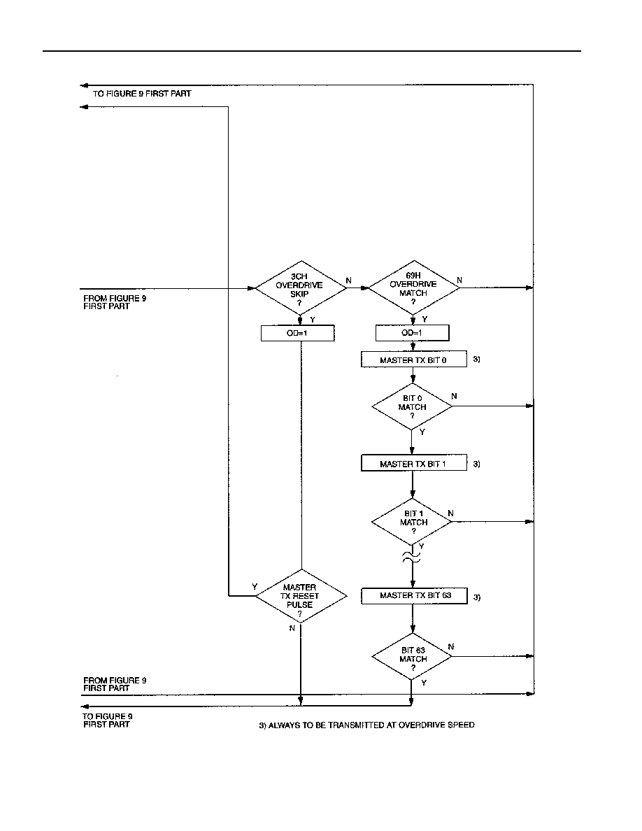
ROM FUNCTION COMMANDS
Once the bus master has detected a presence, it can issue one of the six ROM function commands. All
ROM function commands are eight bits long. A list of these commands follows (refer to flowchart in
Figure 9):
READ ROM [33H]
This command allows the bus master to read the DS2433's 8-bit family code, unique 48-bit serial
number, and 8-bit CRC. This command can only be used if there is a single DS2433 on the bus. If more
than one slave is present on the bus, a data collision will occur when all slaves try to transmit at the same
time (open drain will produce a wired-AND result). The resultant family code and 48-bit serial number
will result in a mismatch of the CRC.
MATCH ROM [55H]
The match ROM command, followed by a 64-bit ROM sequence, allows the bus master to address a
specific DS2433 on a multidrop bus. Only the DS2433 that exactly matches the 64-bit ROM sequence
will respond to the following memory function command. All slaves that do not match the 64-bit ROM
sequence will wait for a Reset Pulse. This command can be used with a single or multiple devices on the
bus.
SKIP ROM [CCH]
This command can save time in a single drop bus system by allowing the bus master to access the
memory functions without providing the 64-bit ROM code. If more than one slave is present on the bus
and a read command is issued following the Skip ROM command, data collision will occur on the bus as
multiple slaves transmit simultaneously (open drain pulldowns will produce a wired-AND result).
SEARCH ROM [F0H]
When a system is initially brought up, the bus master might not know the number of devices on the 1-
Wire bus or their 64-bit ROM codes. The search ROM command allows the bus master to use a process
of elimination to identify the 64-bit ROM codes of all slave devices on the bus. The search ROM process
is the repetition of a simple 3-step routine: read a bit, read the complement of the bit, then write the
desired value of that bit. The bus master performs this simple, 3-step routine on each bit of the ROM.
After one complete pass, the bus master knows the contents of the ROM in one device. The remaining
number of devices and their ROM codes may be identified by additional passes. See Chapter 5 of the
Book of DS19xx iButton Standards for a comprehensive discussion of a search ROM, including an actual
example.
OVERDRIVE SKIP ROM [3CH]
On a single-drop bus this command can save time by allowing the bus master to access the memory
functions without providing the 64-bit ROM code. Unlike the normal Skip ROM command the
Overdrive Skip ROM sets the DS2433 in the Overdrive Mode (OD = 1). All communication following

DS2433
12 of 19
this command has to occur at Overdrive Speed until a Reset Pulse of minimum 480
µ
s duration resets all
devices on the bus to regular speed (OD = 0).
When issued on a multidrop bus this command will set all Overdrive-supporting devices into Overdrive
mode. To subsequently address a specific Overdrive-supporting device, a Reset Pulse at Overdrive speed
has to be issued followed by a Match ROM or Search ROM command sequence. This will speed up the
time for the search process. If more than one slave supporting Overdrive is present on the bus and the
Overdrive Skip ROM command is followed by a read command, data collision will occur on the bus as
multiple slaves transmit simultaneously (open drain pulldowns will produce a wire-AND result).
OVERDRIVE MATCH ROM [69H]
The Overdrive Match ROM command, followed by a 64-bit ROM sequence transmitted at Overdrive
Speed, allows the bus master to address a specific DS2433 on a multidrop bus and to simultaneously set it
in Overdrive Mode. Only the DS2433 that exactly matches the 64-bit ROM sequence will respond to the
subsequent memory function command. Slaves already in Overdrive mode from a previous Overdrive
Skip or Match command will remain in Overdrive mode. All overdrive-capable slaves will return to
regular speed at the next Reset Pulse of minimum 480
µ
s duration. The Overdrive Match ROM
command can be used with a single or multiple devices on the bus.

DS2433
13 of 19
ROM FUNCTIONS FLOW CHART Figure 9 (First Part)
DS2433
14 of 19
ROM FUNCTIONS FLOW CHART Figure 9 (continued)
DS2433
15 of 19
1-WIRE SIGNALING
The DS2433 requires strict protocols to insure data integrity. The protocol consists of four types of
signaling on one line: Reset Sequence with Reset Pulse and Presence Pulse, Write 0, Write 1 and Read
Data. All these signals except Presence Pulse are initiated by the bus master. The DS2433 can
communicate at two different speeds, regular speed and Overdrive Speed. If not explicitly set into the
overdrive mode, the DS2433 will communicate at regular speed. While in Overdrive Mode the fast
timing applies to all wave forms.
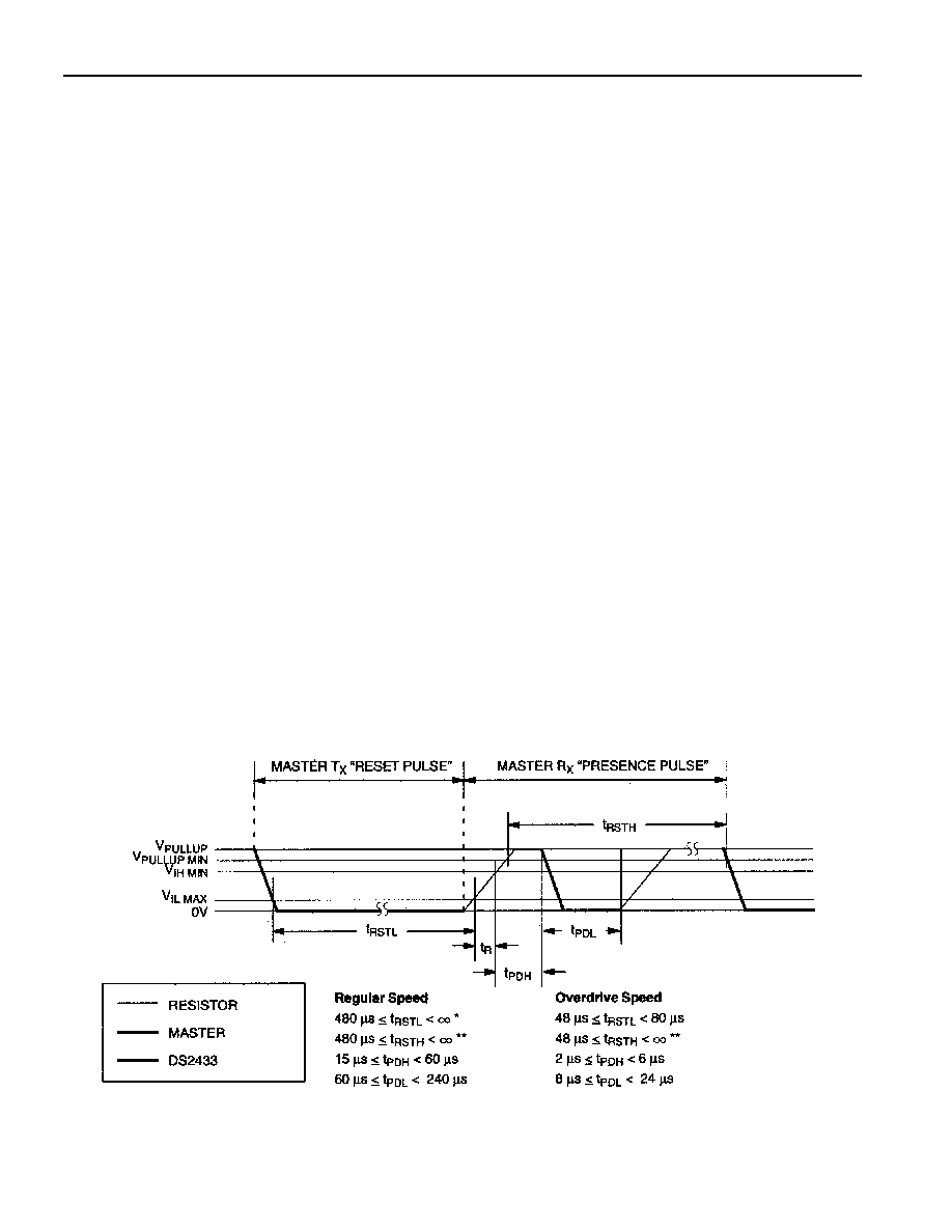
The initialization sequence required to begin any communication with the DS2433 is shown in Figure 10.
A Reset Pulse followed by a Presence Pulse indicates the DS2433 is ready to send or receive data given
the correct ROM command and memory function command. The bus master transmits (TX) a Reset
Pulse (t
RSTL
, minimum 480
µ
s at regular speed, 48
µ
s at Overdrive Speed). The bus master then releases
the line and goes into receive mode (RX). The 1-Wire bus is pulled to a high state via the pullup resistor.
After detecting the rising edge on the data pin, the DS2433 waits (t
PDH
, 15-60
µ
s at regular speed, 2-6
µ
s
at Overdrive speed) and then transmits the Presence Pulse (t
PDL
, 60-240
µ
s at regular speed, 8-24
µ
s at
Overdrive Speed).
A Reset Pulse of 480
µ
s or longer will exit the Overdrive Mode returning the device to regular speed. If
the DS2433 is in Overdrive Mode and the Reset Pulse is no longer than 80
µ
s the device will remain in
Overdrive Mode.
READ/WRITE TIME SLOTS
The definitions of write and read time slots are illustrated in Figure 11. All time slots are initiated by the
master driving the data line low. The falling edge of the data line synchronizes the DS2433 to the master
by triggering a delay circuit in the DS2433. During write time slots, the delay circuit determines when
the DS2433 will sample the data line. For a read data time slot, if a "0" is to be transmitted, the delay
circuit determines how long the DS2433 will hold the data line low overriding the 1 generated by the
master. If the data bit is a "1", the device will leave the read data time slot unchanged.
INITIALIZATION PROCEDURE RESET AND PRESENCE PULSES Figure 10
*In order not to mask interrupt signalling by other devices on the 1-Wire bus, t
RSTL
+ t
R
should always be less than 960 µs.
** Includes recovery time.

DS2433
16 of 19
READ/WRITE TIMING DIAGRAM Figure 11
Write-one Time Slot
Write-zero Time Slot
Read-data Time Slot
CRC GENERATION
With the DS2433 there are two different types of CRCs (Cyclic Redundancy Checks). One CRC is an 8-
bit type and is stored in the most significant byte of the 64-bit ROM. The bus master can compute a CRC

DS2433
17 of 19
value from the first 56 bits of the 64-bit ROM and compare it to the value stored within the DS2433 to
determine if the ROM data has been received error-free by the bus master. The equivalent polynomial
function of this CRC is: X
8
+ X
5
+ X
4
+ 1. This 8-bit CRC is received in the true (non-inverted) form when
reading the ROM of the DS2433. It is computed at the factory and lasered into the ROM.
The other CRC is a 16-bit type, generated according to the standardized CRC16-polynomial function x
16
+
x
15
+x
2
+ 1. This CRC is used for fast verification of a data transfer when writing to the scratchpad. It is
the same type of CRC as is used with NV RAM based iButtons for error detection within the iButton
Extended File Structure. In contrast to the 8-bit CRC, the 16-bit CRC is always returned or sent in the
complemented (inverted) form. A CRC-generator inside the DS2433 chip (Figure 12) will calculate a
new 16-bit CRC as shown in the command flow chart of Figure 7. The bus master compares the CRC
value read from the device to the one it calculates from the data and decides whether to continue with an
operation.
With the Write Scratchpad command the CRC is generated by first clearing the CRC generator and then
shifting in the command code, the Target Addresses TA1 and TA2 and all the data bytes. The DS2433
will transmit this CRC only if the data bytes written to the scratchpad include scratchpad ending offset
11111b. The data may start at any location within the scratchpad.
For more details on generating CRC values including example implementations in both hardware and
software, see the Book of DS19xx iButton Standards.
CRC-16 HARDWARE DESCRIPTION AND POLYNOMIAL Figure 12
(Polynomial X
16
+ X
15
+ X
2
+ 1)
DS2433
18 of 19
ABSOLUTE MAXIMUM RATINGS*
Voltage on Any Pin Relative to Ground
-0.5V to +7.0V
Operating Temperature
-40
∞
C to +85
∞
C
Storage Temperature
-55
∞
C to +125
∞
C
Soldering Temperature
260
∞
C for 10 seconds
* This is a stress rating only and functional operation of the device at these or any other conditions above
those indicated in the operation sections of this specification is not implied. Exposure to absolute
maximum rating conditions for extended periods of time may affect reliability.
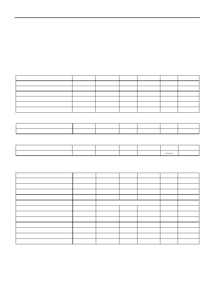
DC ELECTRICAL CHARACTERISTICS
(V
PUP
=2.8V to 6.0V; -40∞C to +85∞C)
PARAMETER
SYMBOL
MIN
TYP
MAX
UNITS
NOTES
Logic 1
V
IH
2.2
V
1, 8
Logic 0
V
IL
-0.3
+0.8
V
1, 9
Output Logic Low @ 4 mA
V
OL
0.4
V
1
Output Logic High
V
OH
V
PUP
6.0
V
1, 2
Input Load Current
I
L
5
µ
A
3
Programming Current
I
LPROG
500
µ
A
10
CAPACITANCE
(T
A
= 25∞C)
PARAMETER
SYMBOL
MIN
TYP
MAX
UNITS
NOTES
I/O (1-Wire)
C
IN/OUT
100
800
pF
6
ENDURANCE
(V
PUP
=5.0V; T
A
= 25
∞
C)
PARAMETER
SYMBOL
MIN
TYP
MAX
UNITS
NOTES
Write/Erase Cycles
N
CYCLE
50k
11
AC ELECTRICAL CHARACTERISTICS
REGULAR SPEED
(V
PUP
=2.8V to 6.0V; -40
∞
C to +85
∞
C)
PARAMETER
SYMBOL
MIN
TYP
MAX
UNITS
NOTES
Time Slot
t
SLOT
60
120
µ
s
Write 1 Low Time
t
LOW1
1
15
µ
s
Write 0 Low Time
t
LOW0
60
120
µ
s
Read Low Time
t
LOWR
1
15
µ
s
Read Data Valid
t
RDV
exactly 15
µ
s
Release Time
t
RELEASE
0
15
45
µ
s
Read Data Setup
t
SU
1
µ
s
5
Recovery Time
t
REC
1
µ
s
Reset Time High
t
RSTH
480
µ
s
4
Reset Time Low
t
RSTL
480
µ
s
7
Presence Detect High
t
PDHIGH
15
60
µ
s
Presence Detect Low
t
PDLOW
60
240
µ
s

DS2433
19 of 19
AC ELECTRICAL CHARACTERISTICS
OVERDRIVE SPEED
(V
PUP
=2.8V to 6.0V;-40
∞
C to +85
∞
C)
PARAMETER
SYMBOL
MIN
TYP
MAX
UNITS
NOTES
Time Slot
t
SLOT
6
16
µ
s
Write 1 Low Time
t
LOW1
1
2
µ
s
Write 0 Low Time
t
LOW0
6
16
µ
s
Read Low Time
t
LOWR
1
2
µ
s
Read Data Valid
t
RDV
exactly 2
µ
s
Release Time
t
RELEASE
0
1.5
4
µ
s
Read Data Setup
t
SU
1
µ
s
5
Recovery Time
t
REC
1
µ
s
Reset Time High
t
RSTH
48
µ
s
4
Reset Time Low
t
RSTL
48
80
µ
s
Presence Detect High
t
PDHIGH
2
6
µ
s
Presence Detect Low
t
PDLOW
8
24
µ
s
NOTES:
1.
All voltages are referenced to ground.
2.
V
PUP
= external pullup voltage.
3.
Input load is to ground.
4.
An additional reset or communication sequence cannot begin until the reset high time has expired.
5.
Read data setup time refers to the time the host must pull the 1-Wire bus low to read a bit. Data is
guaranteed to be valid within 1
µ
s of this falling edge.
6.
Capacitance on the data pin could be 800 pF when power is first applied. If a 5 k
resistor is used to
pull up the data line to V
PUP
, 5
µ
s after power has been applied the parasite capacitance will not affect
normal communications.
7.
The reset low time (t
RSTL
) should be restricted to a maximum of 960
µ
s, to allow interrupt signaling,
otherwise, it could mask or conceal interrupt pulses.
8.
V
IH
is a function of the external pullup resistor and V
PUP
.
9.
Under certain low voltage conditions V
ILMAX
may have to be reduced to as much as 0.5V to always
guarantee a Presence Pulse.
10.
The Copy Scratchpad takes 5 ms maximum during which the voltage on the 1-Wire bus must not fall
below 2.8V.
11.
During the execution of the Copy Scratchpad command the DS2433 automatically erases the memory
locations to be written to. No extra steps need to be taken by the bus master.