 | ÐлекÑÑоннÑй компоненÑ: DS2703UT | СкаÑаÑÑ:  PDF PDF  ZIP ZIP |
Äîêóìåíòàöèÿ è îïèñàíèÿ www.docs.chipfind.ru
1 of 20
REV: 071805
Note: Some revisions of this device may incorporate deviations from published specifications known as errata. Multiple revisions of any device
may be simultaneously available through various sales channels. For information about device errata, click here:
www.maxim-ic.com/errata
.
GENERAL DESCRIPTION
The DS2703 provides a robust cryptographic solution
to ensure the authenticity of Li-Ion battery packs for
cell phone, PDA, and portable computing devices.
The DS2703 employs the Secure Hash Algorithm
(SHA-1) specified in the Federal Information
publication 180-1 and 180-2, and ISO/IEC 10118-3.
SHA-1 is designed for authentication
¾just what is
required for identifying battery packs manufactured
by authorized sources.
The device's SHA-1 engine processes a host
transmitted challenge using its stored 64-bit secret
key and unique 64-bit ROM ID to produce a 160-bit
response word for transmission back to the host. The
secret key is securely stored on-chip and never
transmitted between the battery and the host. A
DS2703-based system produces a high degree of
authentication security between a host system and its
removable battery or other peripheral devices.
The Thermistor Multiplexer feature allows a three
contact battery pack configuration to support data
and thermistor functions. When activated through
1-Wire command, the THM pin presents the
thermistor impedance on the data contact and
disconnects internal loading from the node.
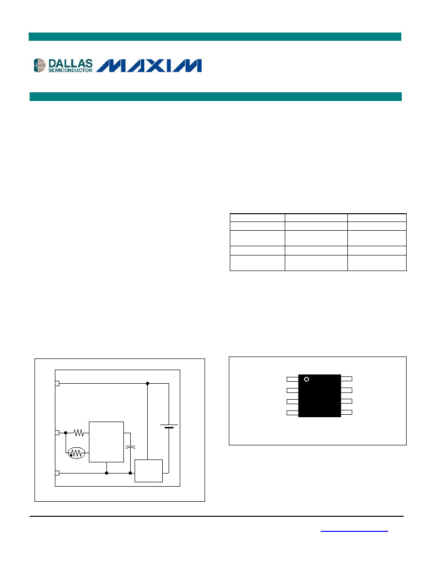
TYPICAL OPERATING CIRCUIT
DS2703
VSS
DQ
DATA
PACK +
PACK -
VB
150
W
Li-Ion
Protection
THM
BATTERY PACK
0.22
mF
FEATURES
§
Secure Challenge and Response Authentication
Using the SHA-1 Algorithm
§
Directly Powered by the Dallas 1-Wire
®
Interface
with 16kpbs Standard and 143kpbs Overdrive
Communication Modes
§
Unique 64-Bit Serial Number
§
Thermistor Multiplexer
§
Operates with V
PULLUP
as Low as 2.7V
§
mMax-8 Package (Lead-Free)
ORDERING INFORMATION
PART TEMP
RANGE
PIN-PACKAGE
DS2703U
-20
°C to +70°C
mMax-8
DS2703U/T&R
-20
°C to +70°C
DS2703U on
Tape-and-Reel
DS2703U+
-20
°C to +70°C
mMax-8
DS2703U+T&R
-20
°C to +70°C
DS2703U+ on
Tape-and-Reel
+ Denotes lead-free package.
APPLICATIONS
2.5G/3G Wireless Handsets
PDAs
Handheld or Notebook Computers and Terminals
Digital Still and Video Cameras
PIN CONFIGURATION
DS2703
SHA-1 Battery Pack
Authentication IC
www.maxim-ic.com
TOP VIEW
mMAX
DS2703U+
VSS
NC
NC
NC
NC
VB
DQ
THM
6
8
7
5
3
1
2
4
1-Wire is a registered trademark of Dallas Semiconductor.
DS2703 SHA-1 Battery Pack Authentication IC
2 of 20
ABSOLUTE MAXIMUM RATINGS
Voltage Range on DQ, THM Pins Relative to Ground
-0.3V to +18V
Voltage Range on VB Pin Relative to Ground
-0.3V to +6V
Operating Temperature Range
-40°C to +85°C
Storage Temperature Range
-55°C to +125°C
Soldering Temperature
See IPC/JEDEC J-STD-020A Specification
Stresses beyond those listed under "Absolute Maximum Ratings" may cause permanent damage to the device. These are stress ratings only,
and functional operation of the device at these or any other conditions beyond those indicated in the operational sections of the specifications is
not implied. Exposure to the absolute maximum rating conditions for extended periods may affect device.
RECOMMENDED DC OPERATING CONDITIONS
(T
A
= -20°C to +70°C.)
PARAMETER SYMBOL CONDITIONS MIN
TYP
MAX
UNITS
Communication Mode
0
5.5
DQ Pullup Voltage
V
PULLUP
Computation Mode
2.7
5.5
V
DQ, THM Relative Voltage
V
DQ-THM
(Note
1)
-0.3
15
V
DQ to THM Resistor
R
DQ-THM
(Note 2)
5 500 KW
DC ELECTRICAL CHARACTERISTICS
(V
PULLUP
= 2.7V to 5.5V, T
A
= -20°C to +70°C.)
PARAMETER SYMBOL CONDITIONS MIN
TYP
MAX
UNITS
I
DQ1
Communication
Mode
5
mA
I
DQ2
Computation Mode,
SHA-1 Computation Active
0.5
mA
I
DQ3
Thermistor Mux Active,
(Note 3)
1
mA
I
PP
14.5 < V(DQ) < 15.0V
0 < t < 50
o
C
10
mA
DQ Load Current
I
PP-IDLE
(Note
4)
60
mA
DQ Programming Voltage
V
PP
Program Pulse, (Note 5, 6)
14.5
15.0
V
Input Logic High: DQ
V
IH
(Note 6)
0.8 V
PULLUP
V
Input Logic Low: DQ
V
IL
(Note
6)
0.5 V
Output Logic Low: DQ
V
OL-DQ
I
OL
= 4mA, (Note 6, 7)
0.4 V
Output Logic Low: THM
V
OL-THM
I
OL
= 4mA, (Note 6, 7, 8)
0.4 V
Hold-Up Current: VB pin
I
HU
THM pin Active, V
B
= 2.70V
3.2
mA
DQ Capacitance
C
DQ
(Note
9)
50
pF
EEPROM RELIABILITY SPECIFICATION
(V
PULLUP
= 2.7V to 5.5V, T
A
= -20°C to +70°C.)
PARAMETER
SYMBOL CONDITIONS MIN
TYP
MAX
UNITS
EEPROM Write Endurance
N
EEC
0 < t < 50
o
C (Note 10)
1000
Cycles

DS2703 SHA-1 Battery Pack Authentication IC
3 of 20
AC ELECTRICAL CHARACTERISTICS
(V
PULLUP
= 2.7V to 5.5V, T
A
= -20°C to +70°C.)
PARAMETER
SYMBOL CONDITIONS MIN
TYP
MAX
UNITS
THM Low Delay
t
TD
(Note
11)
15
ms
Computation Delay Time
t
D
(Note 12)
100
µs
Computation Time
t
SHA
(Note 12)
15
ms
Programming Pulse Width
t
PPW
(Note 5)
17
ms
Programming Pulse Rise Time
t
PPR
0.5
5
µs
Programming Pulse Fall Time
t
PPF
0.5
5
µs
Start-up Delay Time
t
STRT
(Note 13)
100
ms
AC ELECTRICAL CHARACTERISTICS: 1-Wire INTERFACE
(V
PULLUP
= 2.7V to 5.5V, T
A
= -20°C to +70°C.)
PARAMETER
SYMBOL CONDITIONS MIN
TYP
MAX
UNITS
1-Wire INTERFACE REGULAR TIMING
Time Slot
t
SLOT
60
120
µs
Recovery Time
t
REC
1
µs
Write 0 Low Time
t
LOW0
60
120
µs
Write 1 Low Time
t
LOW1
1
15
µs
Read Data Valid Time
t
RDV
15
µs
Reset Time High
t
RSTH
480
µs
Reset Time Low
t
RSTL
480
960
µs
Presence Detect High
t
PDH
15
60
µs
Presence Detect Low
t
PDL
60
240
µs
1-Wire INTERFACE OVERDRIVE TIMING
Time Slot
t
SLOT
6
16
µs
Recovery Time
t
REC
1
µs
Write 0 Low Time
t
LOW0
6
16
µs
Write 1 Low Time
t
LOW1
1
2
µs
Read Data Valid Time
t
RDV
2
µs
Reset Time High
t
RSTH
48
µs
Reset Time Low
t
RSTL
48
80
µs
Presence Detect High
t
PDH
2
6
µs
Presence Detect Low
t
PDL
8
24
µs
Note 1:
V
DQ
V
THM
. The THM pin must not be driven to a higher voltage than the DQ pin.
Note 2:
The application thermistor cannot exceed the R
DQ-THM
resistance range over operating temperature. If thermistor mode is not used in the application, it is
recommended that a 50K resistor be connected between DQ and THM pins instead.
Note 3:
Maximum leakage of DQ pin while in thermistor mode.
Note 4:
When performing a Lock Secret (0x6A), Set Overdrive (0x8B) or Clear Overdrive (0x8D) operation, there will be an increased operating current of I
PGM-
IDLE
during the time period from when the command is issued until the next 1-Wire bus reset. I
PGM-IDLE
current will be present before and after the program
pulse.
Note 5:
See Figure 11 for definitionof t
PPR
, t
PPW
, and t
PPF.
Note 6:
All voltages referenced to VSS.
Note 7:
V
DQ
must be at least 3.0V when the 1-Wire bus is idle.
Note 8:
Drive strength at time=0 after Activate Thermistor command is sent to the DS2703.
Note 9:
Does not include capacitance referred from VB pin on initial power up.
Note 10: EEPROM data read retention is four years at +50°C
Note 11: Time from msb of Activate Thermistor command until THM pin is driven low internally.
Note 12: Time from msb of Compute Next Secret or Compute MAC command.
Note 13: Time after initial power up before the DS2703 will respond to communication. T
STRT
specifications are valid only if the capacitor on VB (C
VB
) is 0.22µF.
Worst case 100ms delay based on maximum thermistor value of 500k.
DS2703 SHA-1 Battery Pack Authentication IC
4 of 20
PIN DESCRIPTION
PIN NAME
FUNCTION
1 THM
Thermistor Mux. Connect a thermistor from THM to DQ. Optional. For temperature
measurements only. If a thermistor is not used in the application, It is recommended THM
be tied to DQ with a 50K resistor instead. THM should never be left floating.
2 VSS
Device Ground. Connect directly to the negative terminal of the battery cell.
3 DQ
Data Input/Output. 1-Wire data line. Open-drain output driver. Connect this pin to the
DATA terminal of the battery pack. This pin has a weak internal pulldown (1µA Typical).
4 VB
Hold-up Supply Bypass Input. Internal power supply to the DS2703 while DQ is low.
Connect a 0.22µF capacitor from VB to V
SS
.
5 NC
No Connect. Pin not connected internally, float or connect to VSS.
6 NC
No Connect. Pin not connected internally, float or connect to VSS.
7 NC
No Connect. Pin not connected internally, float or connect to VSS.
8 NC
No Connect. Pin not connected internally, float or connect to VSS.
Figure 1. Block Diagram
1-Wire
Interface
Command
Processor
2 x 32 bit
Rom ID
EEPROM
Write Control
VB
DQ
THM
2 x 32 bit
Challenge
SHA-1
Engine
2 x 32-bit
Secret
MAC Buffer
(Registers
A - E)
VSS
Fixed Data
& Constants
Response
Timing
Generator
To Command
Processor
Driver
V
DD_INT

DS2703 SHA-1 Battery Pack Authentication IC
5 of 20
DETAILED DESCRIPTION
The DS2703 is comprised of a SHA-1 Authentication function and thermistor mux control that are accessed via a 1-
Wire interface. The high voltage (HV) detection circuit routes the externally supplied programming voltage to the
EEPROM array and enables the internal regulator to isolate portions of the chip from the programming voltage. The
1-Wire interface controls access by a host system to the 64-bit Net Address (ROM ID) and SHA-1 Authentication.
The DS2703 operates in one of four operating modes: communication, computation, programming and thermistor
access. Most operations are performed in communication mode, with the host system addressing the DS2703
using Net Address commands and then setting up an authentication exchange and retrieving the results. In
communication mode, the DQ load current averages 5
mA maximum, and the DS2703 can be "parasite" powered
via the DQ pin through a high impedance pullup resistor during a communication transaction. Power available while
the 1-Wire bus is at a logic high is rectified by the on chip diode and stored in an off chip capacitor connected to the
VB pin. The voltage regulator operates in a low impedance drop-out mode in the communication mode.
In computation mode, when a SHA-1 verification is performed, the DQ load current increases up to 1mA,
necessitating a lower impedance pullup resistor. The computation mode load current occurs after the host supplies
the required challenge data and requests the computation using the proper function commands in communication
mode. In this mode, the pullup supply and low impedance pullup resistor must be capable of keeping the DQ pin
above V
PULLUP-MIN
. The voltage regulator operates in a low impedance drop-out mode.
The third operating mode is required when programming the non-volatile memory portions of the DS2703. The
programming mode is defined by the application of a high voltage programming pulse to the DQ pin at the
appropriate point during a Compute Secret command, Load/Lock Secret or Clear/Set Overdrive Timing command.
The internal voltage regulator limits the internal voltage (V
DD_INT
) to isolate low voltage portions of the chip from the
HV programming pulse. Typically, programming mode is used during module or pack manufacture to configure the
DS2703 and program the 64-bit secret.
Finally, thermistor mode allows the voltage on an external thermistor to be measured from the DQ line. The
command sequence causes the DS2703 to internally disconnect its DQ interface and drive the THM pin to VSS
allowing the measurement to be made. The IC remains in this mode until the VB pin capacitor is drained causing
the DS2703 to power cycle back to communication mode.
AUTHENTICATION
Authentication is performed using a FIPS-180 compliant SHA-1 one way hash algorithm on a 512 bit message
block. The message block consists of a 64-bit secret, a 64-bit challenge and 384 bits of constant data. Optionally,
the 64-bit net address replaces 64 of the 384 bits of constant data used in the hash operation. An authentication
attempt is initiated by the host system providing a 64-bit random challenge then sending one of two compute
command sequences. The host and the DS2703 both calculate the result based on the mutually known secret. The
result data, known as the Message Authentication Code (MAC) or Message Digest, is returned by the DS2703 for
comparison to the host's result. Note that the secret is never transmitted on the bus and thus cannot be captured
by observing bus traffic. SHA-1 based authentication is a cryptographically strong method in wide use for digitally
signing encrypted files and secure transactions such as electronic cash and password exchange protocols.
The FIPS 180 Compliant Input Block, the 512-bit message block is organized as sixteen 32-bit words, W0-W15.
The message block is initialized when a command is received to compute the MAC. Upon initialization, the 64-bit
secret is loaded, and it is important to note that the SHA-1 algorithm has access to this data, but not the serial
interface. The challenge data is received with the command just prior to the compute MAC command. The
challenge data is cleared during computation of the MAC, so the host must write new challenge data prior to
issuing each Compute MAC or Compute Next Secret command. Additionally, the A, B, C, D and E variables used
in the hash computation are initialized per FIPS 180 as shown in Table 1. Variable Initiation.