 | –≠–ª–µ–∫—Ç—Ä–æ–Ω–Ω—ã–π –∫–æ–º–ø–æ–Ω–µ–Ω—Ç: DS2761BE | –°–∫–∞—á–∞—Ç—å:  PDF PDF  ZIP ZIP |

1 of 24
072303
FEATURES
ß Lithium-Ion (Li+) Safety Circuit
- Overvoltage Protection
- Overcurrent/Short-Circuit Protection
- Undervoltage Protection
ß Zero Volt Battery Recovery Charge
ß Available in Two Configurations:
- Internal 25m
W Sense Resistor
- External User-Selectable Sense Resistor
ß Current Measurement
- 12-Bit Bidirectional Measurement
- Internal Sense Resistor Configuration:
0.625mA LSB and ±1.9A Dynamic Range
- External Sense Resistor Configuration:
15.625
mV LSB and ±64mV Dynamic
Range
ß Current Accumulation:
- Internal Sense Resistor: 0.25mAhr LSB
- External Sense Resistor: 6.25
mVhr LSB
ß Voltage Measurement with 4.88mV
Resolution
ß Temperature Measurement Using Integrated
Sensor with 0.125
∞C Resolution
ß System Power Management and Control
Feature Support
ß 32 Bytes of Lockable EEPROM
ß 16 Bytes of General-Purpose SRAM
ß Dallas 1-Wire
Æ
Interface with Unique 64-bit
Device Address
ß Low Power Consumption:
- Active Current: 60
mA typ, 90mA max
- Sleep Current:
1
mA typ, 2mA max
PIN CONFIGURATION
PIN DESCRIPTION
CC
- Charge Control Output
DC
- Discharge Control Output
DQ - Data Input/Output
PIO - Programmable I/O Pin
PLS - Battery Pack Positive Terminal Input
PS
- Power Switch Sense Input
V
IN
- Voltage-Sense Input
V
DD
- Power-Supply Input (2.5V to 5.5V)
V
SS
- Device Ground
SNS - Sense Resistor Connection
IS1 - Current-Sense Input
IS2 - Current-Sense Input
SNS Probe
- Do Not Connect
V
SS
Probe
- Do Not Connect
DS2761
High-Precision Li+ Battery Monitor
www.maxim-ic.com
CC
V
IN
V
DD
PIO
V
SS
V
SS
V
SS
PS
IS1
DS2761
16-Pin TSSOP Package
IS2
SNS
SNS
1
2
2
3
2
1
4
5
6
7
8
16
15
14
13
12
11
10
9
SNS
DQ
PLS
DC
1-Wire is a registered trademark of Dallas Semiconductor.
DS2761
Flip-Chip Packaging*
Top View
PLS DC DQ
CC IS2
VIN IS1
VDD PIO PS
SNS
VSS
1 2 3 4
A
B
C
D
E
F
SNS
Probe
VSS
Probe
* Mechanical drawing for the 16-pin TSSOP and DS2761 flip-chip package can be found at:
http://pdfserv.maxim-ic.com/arpdf/Packages/16tssop.pdf
http://pdfserv.maxim-ic.com/arpdf/Packages/chips/2761x.pdf

DS2761
2 of 24
ORDERING INFORMATION
PART
MARKING DESCRIPTION
DS2761AE
D2761EA
TSSOP, External Sense Resistor, 4.275V V
OV
DS2761BE
D2761EB
TSSOP, External Sense Resistor, 4.35V V
OV
DS2761AE/T&R
D2761EA
DS2761AE on Tape-and-Reel
DS2761BE/T&R
D2761EB
DS2761BE on Tape-and-Reel
DS2761AE-025
2761A25
TSSOP, 25m
W Sense Resistor, 4.275V V
OV
DS2761BE-025
2761B25
TSSOP, 25m
W Sense Resistor, 4.35V V
OV
DS2761AE-025/T&R 2761A25
DS2761AE-025 in Tape-and-Reel
DS2761BE-025/T&R 2761B25
DS2761BE-025 in Tape-and-Reel
DS2761AX-025/T&R DS2761AR Flip-Chip, 25m
W Sense Resistor, Tape-and-Reel, 4.275V V
OV
DS2761BX-025/T&R DS2761BR
Flip-Chip, 25m
W Sense Resistor, Tape-and-Reel, 4.35V V
OV
DS2761AX/T&R
DS2761A
Flip-Chip, External Sense Resistor, Tape-and-Reel, 4.275V V
OV
DS2761BX/T&R
DS2761B
Flip-Chip, External Sense Resistor, Tape-and-Reel, 4.35V V
OV
Note: Additional V
OV
options are available, contact Maxim/Dallas Semiconductor sales.
DESCRIPTION
The DS2761 high-precision Li+ battery monitor is a data-acquisition, information-storage, and safety-
protection device tailored for cost-sensitive battery pack applications. This low-power device integrates
precise temperature, voltage, and current measurement, nonvolatile (NV) data storage, and Li+ protection
into the small footprint of either a TSSOP package or flip-chip package. The DS2761 is a key component
in applications including remaining capacity estimation, safety monitoring, and battery-specific data
storage.
Through its 1-Wire interface, the DS2761 gives the host system read/write access to status and control
registers, instrumentation registers, and general-purpose data storage. Each device has a unique factory-
programmed 64-bit net address that allows it to be individually addressed by the host system, supporting
multibattery operation.
The DS2761 is capable of performing temperature, voltage, and current measurement to a resolution
sufficient to support process monitoring applications such as battery charge control, remaining capacity
estimation, and safety monitoring. Temperature is measured using an on-chip sensor, eliminating the need
for a separate thermistor. Bidirectional current measurement and accumulation are accomplished using
either an internal 25m
W sense resistor or an external device. The DS2761 also features a programmable
I/O pin that allows the host system to sense and control other electronics in the pack, including switches,
vibration motors, speakers, and LEDs.
Three types of memory are provided on the DS2761 for battery information storage: EEPROM, lockable
EEPROM, and SRAM. EEPROM memory saves important battery data in true NV memory that is
unaffected by severe battery depletion, accidental shorts, or ESD events. Lockable EEPROM becomes
ROM when locked to provide additional security for unchanging battery data. SRAM provides
inexpensive storage for temporary data.

DS2761
3 of 24
Figure 1. BLOCK DIAGRAM
1-WIRE
INTERFACE
AND
ADDRESS
THERMAL
SENSE
MUX
VOLTAGE
REFERENCE
ADC
REGISTERS AND
USER MEMORY
25m
W
DQ
CHIP GROUND
+
-
LOCKABLE EEPROM
SRAM
TEMPERATURE
VOLTAGE
CURRENT
ACCUM. CURRENT
STATUS / CONTROL
LI-ION PROTECTION
V
IN
IS1
IS2
SNS
IS2
IS1
V
SS
CC
DC
PLS
PS
PIO
TIMEBASE
INTERNAL SENSE RESISTOR CONFIGURATION ONLY
I
TST
I
TST
I
RC
V
DD
V
SS
PLS
TEST CURRENT AND RECOVERY CHARGE DETAIL

DS2761
4 of 24
Table 1. DETAILED PIN DESCRIPTION
SYMBOL
TSSOP
FLIP
CHIP
DESCRIPTION
CC
1
C1
Charge Protection Control Output. Controls an external p-channel
high-side charge protection FET.
DC
3
B2
Discharge Protection Control Output. Controls an external p-channel
high-side discharge protection FET.
DQ
7
B4
Data Input/Out. 1-Wire data line. Open-drain output driver. Connect
this pin to the DATA terminal of the battery pack. Pin has an internal
1
mA pull-down for sensing disconnection.
PIO
14
E2
Programmable I/O Pin. Used to control and monitor user-defined
external circuitry. Open drain to VSS.
PLS
2
B1
Battery Pack Positive Terminal Input. The DS2761 monitors the pack
plus terminal through PLS to detect overcurrent and overload conditions,
as well as the presence of a charge source. Additionally, a charge path to
recover a deeply depleted cell is provided from PLS to V
DD
. In sleep
mode (with SWEN = 0), any capacitance or voltage source connected to
PLS is discharged internally to V
SS
through 200
mA (nominal) to assure
reliable detection of a valid charge source. For details of other internal
connections to PLS and associated conditions see the Li+ Protection
Circuitry section.
PS
10
E4
Power Switch Sense Input. The device wakes up from Sleep Mode
when it senses the closure of a switch to VSS on this pin. Pin has an
internal 1
mA pull-up to V
DD
.
VIN
16
D1
Voltage Sense Input. The voltage of the Li+ cell is monitored via this
input pin. This pin has a weak pullup to V
DD
.
V
DD
15
E1
Power Supply Input. Connect to the positive terminal of the Li+ cell
through a decoupling network.
VSS
13,14,
15
F3
Device Ground. Connect directly to the negative terminal of the Li+ cell.
For the external sense resistor configuration, connect the sense resistor
between VSS and SNS.
SNS
4,5,6
A3
Sense Resistor Connection. Connect to the negative terminal of the
battery pack. In the internal sense resistor configuration, the sense resistor
is connected between VSS and SNS.
IS1
9
D4
Current Sense Input. This pin is internally connected to VSS through a
4.7k
W resistor. Connect a 0.1mF capacitor between IS1 and IS2 to
complete a low-pass input filter.
IS2
8
C4
Current Sense Input. This pin is internally connected to SNS through a
4.7k
W resistor.
SNS
Probe
N/A
C2
Do Not Connect.
VSS
Probe
N/A
D2
Do Not Connect.
DS2761
5 of 24
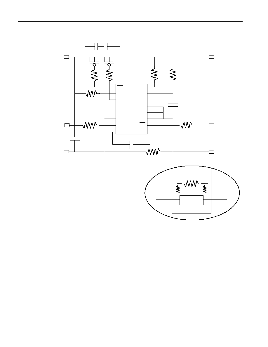
Figure 2. APPLICATION EXAMPLE
1) R
SNS
is present for external sense resistor configurations only.
2) R
SNS-INT
is present for internal sense resistor configurations only.
CC
PLS
DC
SNS
SNS
SNS
DQ
IS2
V
IN
V
DD
PIO
V
SS
V
SS
V
SS
PS
IS1
DS2761
104
102 x 2
104
SNS
DS2761
V
SS
IS2
IS1
4.
7K
W
4.
7K
W
voltage
sense
PACK+
PACK-
DATA
150
W
150
W
1k
W
150
W
1k
W
1k
W
102
BAT+
BAT-
R
SNS
(1)
R
SNS-INT
(2)
R
KS
R
KS
PS
4.7k
W