 | –≠–ª–µ–∫—Ç—Ä–æ–Ω–Ω—ã–π –∫–æ–º–ø–æ–Ω–µ–Ω—Ç: DS3112 | –°–∫–∞—á–∞—Ç—å:  PDF PDF  ZIP ZIP |
1 of 135
081902
Note: Some revisions of this device may incorporate deviations from published specifications known as errata. Multiple revisions of any device
may be simultaneously available through various sales channels. For information about device errata, click here:
http://www.maxim-ic.com/errata
.
.
FEATURES
ß Operates as M13 or E13 multiplexer or as
standalone T3 or E3 framer
ß Flexible multiplexer can be programmed for
multiple configurations including:
-
M13 multiplexing (28 T1 lines into a T3 data
stream)
-
E13 multiplexing (16 E1 lines into an E3 data
stream)
-
E1 to T3 multiplexing (21 E1 lines into a T3
data stream)
ß Two T1/E1 drop and insert ports
ß Supports T3 C-bit parity mode
ß B3ZS/HDB3 encoder and decoder
ß Generates and detects T3/E3 alarms
ß Generates and detects T2/E2 alarms
ß Integrated HDLC controller handles LAPD
messages without host intervention
ß Integrated FEAC controller
ß Integrated BERT supports performance
monitoring
ß T3/E3 and T1/E1 diagnostic (Tx to Rx), line
(Rx to Tx), and payload loopback supported
ß Nonmultiplexed or multiplexed 16-bit control
port (with optional 8-bit mode)
ß 3.3V supply with 5V tolerant I/O
ß Available in 256-pin 1.27mm pitch BGA
package
ß IEEE 1149.1 JTAG support
FUNCTIONAL DIAGRAM
APPLICATIONS
ß Wide Area Network Access Equipment
ß PBXs
ß Access Concentrators
ß Digital Cross-Connect Systems
ß Switches
ß Routers
ß Optical Multiplexers
ß ADMs
ß Test Equipment
ORDERING INFORMATION
PART
PIN-PACKAGE TEMP RANGE
DS3112
256 BGA
0
∞
C to +70
∞
C
DS3112N
256 BGA
-40
∞
C to +85
∞
C
T1/E1
T1/E1
T1/E1
T1/E1
T1/E1
T1/E1
T1/E1
T1/E1
T3/E3
T2/E2
T2/E2
www.maxim-ic.com
DS3112
TEMPE T3/E3 Multiplexer
3.3V T3/E3 Framer and M13/E13/G.747 Mux

DS3112
2 of 135
TABLE OF CONTENTS
1. INTRODUCTION ................................................................................................................................4
2. SIGNAL DESCRIPTION ..................................................................................................................11
2.1 OVERVIEW/SIGNAL PIN LIST...................................................................................................11
2.2 CPU BUS SIGNAL DESCRIPTION..............................................................................................17
2.3 T3/E3 RECEIVE FRAMER SIGNAL DESCRIPTION .................................................................19
2.4 T3/E3 TRANSMIT FORMATTER SIGNAL DESCRIPTION......................................................21
2.5 LOW SPEED (T1 OR E1) RECEIVE PORT SIGNAL DESCRIPTION.......................................23
2.6 LOW SPEED (T1 OR E1) TRANSMIT PORT SIGNAL DESCRIPTION ...................................24
2.7 HIGH SPEED (T3 OR E3) RECEIVE PORT SIGNAL DESCRIPTION......................................26
2.8 HIGH SPEED (T3 OR E3) TRANSMIT PORT SIGNAL DESCRIPTION ..................................26
2.9 JTAG SIGNAL DESCRIPTION.....................................................................................................27
2.10 SUPPLY, TEST, RESET, AND MODE SIGNAL DESCRIPTION ............................................27
3. MEMORY MAP .................................................................................................................................29
4. MASTER DEVICE CONFIGURATION AND STATUS/INTERRUPT......................................31
4.1 MASTER RESET AND ID REGISTER DESCRIPTION..............................................................31
4.2 MASTER CONFIGURATION REGISTERS DESCRIPTION......................................................32
4.3 MASTER STATUS AND INTERRUPT REGISTER DESCRIPTION.........................................37
4.4 TEST REGISTER DESCRIPTION ................................................................................................46
5. T3/E3 FRAMER .................................................................................................................................47
5.1 GENERAL DESCRIPTION ...........................................................................................................47
5.2 T3/E3 FRAMER CONTROL REGISTER DESCRIPTION...........................................................48
5.3 T3/E3 FRAMER STATUS AND INTERRUPT REGISTER DESCRIPTION..............................53
5.4 T3/E3 PERFORMANCE ERROR COUNTERS ............................................................................60
6. M13/E13/G.747 MULTIPLEXER AND T2/E2/G.747 FRAMER ..................................................64
6.1 GENERAL DESCRIPTION ...........................................................................................................64
6.2 T2/E2/G.747 FRAMER CONTROL REGISTER DESCRIPTION................................................64
6.3 T2/E2/G.747 FRAMER STATUS AND INTERRUPT REGISTER DESCRIPTION...................66
6.4 T1/E1 AIS GENERATION CONTROL REGISTER DESCRIPTION..........................................70
7. T1/E1 LOOPBACK AND DROP AND INSERT FUNCTIONALITY .........................................73
7.1 GENERAL DESCRIPTION ...........................................................................................................73
7.2 T1/E1 LOOPBACK CONTROL REGISTER DESCRIPTION......................................................74
7.3 T1 LINE LOOPBACK COMMAND STATUS REGISTER DESCRIPTION ..............................78
7.4 T1/E1 DROP AND INSERT CONTROL REGISTER DESCRIPTION........................................79
8. BERT ...................................................................................................................................................81
8.1 GENERAL DESCRIPTION ...........................................................................................................81
8.2 BERT REGISTER DESCRIPTION................................................................................................81

DS3112
3 of 135
9. HDLC CONTROLLER .....................................................................................................................90
9.1 GENERAL DESCRIPTION ...........................................................................................................90
9.2 HDLC CONTROL AND FIFO REGISTER DESCRIPTION........................................................91
9.3 HDLC STATUS AND INTERRUPT REGISTER DESCRIPTION ..............................................95
10. FEAC CONTROLLER ..................................................................................................................100
10.1 GENERAL DESCRIPTION .......................................................................................................100
10.2 FEAC CONTROL REGISTER DESCRIPTION........................................................................100
10.3 FEAC STATUS REGISTER DESCRIPTION............................................................................102
11. JTAG................................................................................................................................................103
11.1 JTAG DESCRIPTION ................................................................................................................103
11.2 TAP CONTROLLER STATE MACHINE DESCRIPTION......................................................104
11.3 INSTRUCTION REGISTER AND INSTRUCTIONS...............................................................106
11.4 TEST REGISTERS .....................................................................................................................107
12. ELECTRICAL CHARACTERISTICS ........................................................................................113
13. MECHANICAL DIMENSIONS ...................................................................................................124
14. APPLICATIONS AND STANDARDS OVERVIEW .................................................................125
14.1 APPLICATION EXAMPLES .....................................................................................................125
14.2 M13 BASICS...............................................................................................................................126
14.3 E13 BASICS................................................................................................................................132
14.4 G.747 BASICS ............................................................................................................................134

DS3112
4 of 135
1. INTRODUCTION
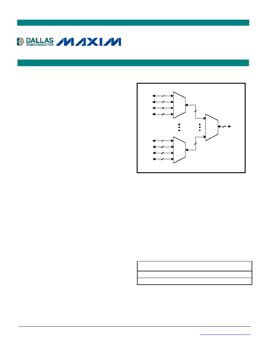
The DS3112 TEMPE (T3 E3 MultiPlexEr) device can be used either as a multiplexer or a T3/E3 framer.
When the device is used as a multiplexer, it can be operated in one of three modes:
M13 ≠ multiplex 28 T1 lines into a T3 data stream
E13 ≠ multiplex 16 E1 lines into a E3 data stream
G.747 ≠ multiplex 21 E1 lines into a T3 data stream
See Figures 1A, 1B, and 1C for block diagrams of these three modes. In each of the block diagrams, the
receive section is at the bottom and the transmit section is at the top. The receive path is defined as
incoming T3/E3 data and the transmit path is defined as outgoing T3/E3 data. When the device is
operated solely as a T3 or E3 framer, the multiplexer portion of the device is disabled and the raw T3/E3
payload will be output at the FRD output and input at the FTD input. See Figures 1A and 1B for details.
In the receive path, raw T3/E3 data is clocked into the device (either in a bipolar or unipolar fashion) with
the HRCLK at the HRPOS and HRNEG inputs. The data is then framed by the T3/E3 framer and passed
through the two-step demultiplexing process to yield the resultant T1 and E1 data streams, which are
output at the LRCLK and LRDAT outputs. In the transmit path, the reverse occurs. The T1 and E1 data
streams are input to the device at the LTCLK and LTDAT inputs. The device will sample these inputs
and then multiplex the T1 and E1 data streams through a two-step multiplexing process to yield the
resultant T3 or E3 data stream. The n this data stream is passed through the T3/E3 formatter to have the
framing overhead added, and the final data stream to be transmitted is output at the HTPOS and HTNEG
outputs using the HTCLK output.
The DS3112 has been designed to meet all of the latest telecommunications standards. Table 1A lists all
of the applicable standards for the device.
The TEMPE device has a number of advanced features such as:
ß the ability to drop and insert up to two T1 or E1 ports
ß an onboard HDLC controller with 256-byte buffers
ß an onboard Bit Error Rate Tester (BERT)
ß advanced diagnostics to create and detect many different types of errors
See Table 1B for a complete list of main features within the device.

DS3112
5 of 135
APPLICABLE STANDARDS Table 1A
1) American National Standard for Telecommunications - ANSI T1.107 ≠ 1995 "Digital Hierarchy -
Formats Specification"
2) American National Standard for Telecommunications - ANSI T1.231 - 199X ≠ Draft "Digital
Hierarchy - Layer 1 In-Service Digital Transmission Performance Monitoring"
3) American National Standard for Telecommunications - ANSI T1.231 ≠ 1993 "Digital Hierarchy -
Layer 1 In-Service Digital Transmission Performance Monitoring"
4) American National Standard for Telecommunications - ANSI T1.404 ≠ 1994 "Network-to-Customer
Installation ≠ DS3 Metallic Interface Specification"
5) American National Standard for Telecommunications - ANSI T1.403 ≠ 1999 "Network and Customer
Installation Interfaces ≠ DS1 Electrical Interface"
6) American National Standard for Telecommunications - ANSI T1.102 ≠ 1993 "Digital Hierarchy ≠
Electrical Interfaces"
7) Bell Communications Research - TR-TSY-000009, Issue 1, May 1986 "Asynchronous Digital
Multiplexes Requirements and Objectives"
8) Bell Communications Research - TR-TSY-000191, Issue 1, May 1986 "Alarm Indication Signal
Requirements and Objectives"
9) Bellcore - GR-499-CORE, Issue 1, December 1995 "Transport Systems Generic Requirements
(TSGR): Common Requirements"
10) Bellcore - GR-820-CORE, Issue 1, November 1994 "Generic Digital Transmission Surveillance"
11) Network Working Group Request for Comments - RFC1407, January, 1993 "Definition of Managed
Objects for the DS3/E3 Interface Type"
12) International Telecommunication Union (ITU) G.703, 1991 "Physical/Electrical Characteristics of
Hierarchical Digital Interfaces
13) International Telecommunication Union (ITU) G.823, March 1993 "The Control of Jitter and Wander
Within Digital Networks Which are Based on the 2048kbps Hierarchy"
14) International Telecommunication Union (ITU) G.742, 1993 "Second Order Digital Multiplex
Equipment Operating at 8448 kbps and Using Positive Justification"
15) International Telecommunication Union (ITU) G.747, 1993 "Second Order Digital Multiplex
Equipment Operating at 6312 kbps and Multiplexing Three Tributaries at 2048kbps"
16) International Telecommunication Union (ITU) G.751, 1993 "Digital Multiplex Equipments Operating
at the Third Order Bit Rate of 34368kbps and Using Positive Justification"
17) International Telecommunication Union (ITU) G.775, November 1994 "Loss Of Signal (LOS) and
Alarm Indication Signal (AIS) Defect Detection and Clearance Criteria"
18) International Telecommunication Union (ITU) O.151, October 1992 "Error Performance Measuring
Equipment Operating at the Primary Rate And Above"
19) International Telecommunication Union (ITU) O.153, October 1992 "Basic Parameters for the
Measurement of Error Performance at Bit Rates Below the Primary Rate"
20) International Telecommunication Union (ITU) O.161, 1984 "In-Service Code Violation Monitors for
Digital Systems"