 | –≠–ª–µ–∫—Ç—Ä–æ–Ω–Ω—ã–π –∫–æ–º–ø–æ–Ω–µ–Ω—Ç: DS3231S | –°–∫–∞—á–∞—Ç—å:  PDF PDF  ZIP ZIP |
General Description
The DS3231 is a low-cost, extremely accurate I
2
C real-
time clock (RTC) with an integrated temperature-
compensated crystal oscillator (TCXO) and crystal. The
device incorporates a battery input, and maintains accu-
rate timekeeping when main power to the device is inter-
rupted. The integration of the crystal resonator enhances
the long-term accuracy of the device as well as reduces
the piece-part count in a manufacturing line. The DS3231
is available in commercial and industrial temperature
ranges, and is offered in a 16-pin, 300-mil SO package.
The RTC maintains seconds, minutes, hours, day, date,
month, and year information. The date at the end of the
month is automatically adjusted for months with fewer
than 31 days, including corrections for leap year. The
clock operates in either the 24-hour or 12-hour format
with an AM/PM indicator. Two programmable time-of-
day alarms and a programmable square-wave output
are provided. Address and data are transferred serially
through an I
2
C bidirectional bus.
A precision temperature-compensated voltage refer-
ence and comparator circuit monitors the status of V
CC
to detect power failures, to provide a reset output, and
to automatically switch to the backup supply when nec-
essary. Additionally, the RST pin is monitored as a
pushbutton input for generating a reset externally.
Applications
Servers
Utility Power Meters
Telematics
GPS
Features
Accuracy ±2ppm from 0∞C to +40∞C
Accuracy ±3.5ppm from -40∞C to +85∞C
Battery Backup Input for Continuous
Timekeeping
Operating Temperature Ranges
Commercial: 0∞C to +70∞C
Industrial: -40∞C to +85∞C
Low-Power Consumption
Real-Time Clock Counts Seconds, Minutes,
Hours, Day, Date, Month, and Year with Leap Year
Compensation Valid Up to 2100
Two Time-of-Day Alarms
Programmable Square-Wave Output
Fast (400kHz) I
2
C Interface
3.3V Operation
Digital Temp Sensor Output: ±3∞C Accuracy
Register for Aging Trim
RST Input/Output
UL Recognized
DS3231
Extremely Accurate I
2
C-Integrated
RTC/TCXO/Crystal
______________________________________________ Maxim Integrated Products
1
Rev 2; 6/05
For pricing, delivery, and ordering information, please contact Maxim/Dallas Direct! at
1-888-629-4642, or visit Maxim's website at www.maxim-ic.com.
Ordering Information
PART
TEMP RANGE
PIN-PACKAGE
TOP
MARK
DS3231S
0∞C to +70∞C
16 SO
DS3231
DS3231SN
-40∞C to +85∞C
16 SO
DS3231N
DS3231S+
0∞C to +70∞C
16 SO
DS3231+
DS3231SN+
-40∞C to +85∞C
16 SO
DS3231N+
Pin Configuration appears at end of data sheet.
Purchase of I
2
C components from Maxim Integrated Products, Inc., or one of its sublicensed Associated Companies, conveys a
license under the Philips I
2
C Patent Rights to use these components in an I
2
C system, provided that the system conforms to the I
2
C
Standard Specification as defined by Philips.
DS3231
V
CC
SCL
R
PU
R
PU
= t
R
/C
B
R
PU
INT/SQW
32kHz
V
BAT
PUSHBUTTON
RESET
SDA
RST
N.C.
N.C.
N.C.
N.C.
V
CC
V
CC
GND
V
CC
CPU
N.C.
N.C.
N.C.
N.C.
Typical Operating Circuit
+Denotes lead-free
DS3231
Extremely Accurate I
2
C-Integrated
RTC/TCXO/Crystal
2
_____________________________________________________________________
ABSOLUTE MAXIMUM RATINGS
RECOMMENDED DC OPERATING CONDITIONS
(T
A
= T
MIN
to T
MAX
, unless otherwise noted.) (Notes 1, 2)
Stresses beyond those listed under "Absolute Maximum Ratings" may cause permanent damage to the device. These are stress ratings only, and functional
operation of the device at these or any other conditions beyond those indicated in the operational sections of the specifications is not implied. Exposure to
absolute maximum rating conditions for extended periods may affect device reliability.
Voltage Range on V
CC
, V
BAT
, 32kHz, SCL, SDA, RST,
INT/SQW Relative to Ground.............................-0.3V to +6.0V
Operating Temperature Range
(noncondensing) .............................................-40∞C to +85∞C
Junction Temperature ......................................................+125∞C
Storage Temperature Range ...............................-40∞C to +85∞C
Lead Temperature
(Soldering, 10s).....................................................+260∞C/10s
Soldering Temperature....................................See the Handling,
PC Board Layout, and Assembly section.
PARAMETER
SYMBOL
CONDITIONS
MIN
TYP
MAX
UNITS
V
CC
2.3
3.3
5.5
V
Supply Voltage
V
BAT
2.3
3.0
5.5
V
Logic 1 Input SDA, SCL
V
IH
0.7 x
V
CC
V
CC
+
0.3
V
Logic 0 Input SDA, SCL
V
IL
-0.3
+0.3 x
V
CC
V
Pullup Voltage
(SDA, SCL, 32kHz, INT/SQW)
V
PU
V
CC
= 0V
5.5V
V
ELECTRICAL CHARACTERISTICS
(V
CC
= 2.3V to 5.5V, V
CC
> V
BAT
, T
A
= T
MIN
to T
MAX
, unless otherwise noted.) (Typical values are at V
CC
= 3.3V, V
BAT
= 3.0V, and
T
A
= +25∞C, unless otherwise noted.) (Notes 1, 2)
PARAMETER
SYMBOL
CONDITIONS
MIN
TYP
MAX
UNITS
V
CC
= 3.63V
200
Active Supply Current
I
CCA
(Notes 3, 4)
V
CC
= 5.5V
300
µA
V
CC
= 3.63V
110
Standby Supply Current
I
CCS
I
2
C bus inactive, 32kHz
output on, SQW output off
(Note 4)
V
CC
= 5.5V
170
µA
V
CC
= 3.63V
575
Temperature Conversion Current
I
CCSCONV
I
2
C bus inactive, 32kHz
output on, SQW output off
V
CC
= 5.5V
650
µA
Power-Fail Voltage
V
PF
2.45
2.575
2.70
V
Logic 0 Output, 32kHz, INT/SQW,
SDA
V
OL
I
OL
= 3mA
0.4
V
Logic 0 Output, RST
V
OL
I
OL
= 1mA
0.4
V
Output Leakage Current 32kHz,
INT/SQW, SDA
I
LO
Output high impedance
-1
0
+1
µA
Input Leakage SCL
I
LI
-1
+1
µA
RST Pin I/O Leakage
I
OL
RST high impedance (Note 5)
-200
+10
µA
V
BAT
Leakage Current
(V
CC
Active)
I
BATLKG
25
100
nA
DS3231
Extremely Accurate I
2
C-Integrated
RTC/TCXO/Crystal
_____________________________________________________________________
3
ELECTRICAL CHARACTERISTICS (continued)
(V
CC
= 2.3V to 5.5V, V
CC
> V
BAT
, T
A
= T
MIN
to T
MAX
, unless otherwise noted.) (Typical values are at V
CC
= 3.3V, V
BAT
= 3.0V, and
T
A
= +25∞C, unless otherwise noted.) (Notes 1, 2)
PARAMETER
SYMBOL
CONDITIONS
MIN
TYP
MAX
UNITS
Output Frequency
f
OUT
V
CC
= 3.3V or V
BAT
= 3.3V
32.768
kHz
0∞C to +40∞C
±2
Frequency Stability vs.
Temperature (Commercial)
f/f
OUT
V
CC
= 3.3V or
V
BAT
= 3.3V,
aging offset = 00h
>40∞C to +70∞C
±3.5
ppm
-40∞C to <0∞C
±3.5
0∞C to +40∞C
±2
Frequency Stability vs.
Temperature (Industrial)
f/f
OUT
V
CC
= 3.3V or
V
BAT
= 3.3V,
aging offset = 00h
>40∞C to +85∞C
±3.5
ppm
Frequency Stability vs. Voltage
f/V
1
ppm/V
-40∞C
0.7
+25∞C
0.1
+70∞C
0.4
Trim Register Frequency
Sensitivity per LSB
f/LSB
Specified at:
+85∞C
0.8
ppm
Temperature Accuracy
Temp
V
CC
= 3.3V or V
BAT
= 3.3V
-3
+3
∞C
First year
±1.0
Crystal Aging
f/f
0
After reflow,
not production tested
0≠10 years
±5.0
ppm
ELECTRICAL CHARACTERISTICS
(V
CC
= 0V, V
BAT
= 2.3V to 5.5V, T
A
= T
MIN
to T
MAX
, unless otherw.ise noted.) (Note 1)
PARAMETER
SYMBOL
CONDITIONS
MIN
TYP
MAX
UNITS
V
BAT
= 3.63V
70
Active Battery Current
I
BATA
EOSC = 0, BBSQW = 0,
SCL = 400kHz (Note 4)
V
BAT
= 5.5V
150
µA
V
BAT
= 3.63V
0.84
3.0
Timekeeping Battery Current
I
BATT
EOSC = 0, BBSQW = 0,
EN32kHz = 1,
SCL = SDA = 0V or
S C L = S D A = V
BAT
( Note 4) V
BAT
= 5.5V
1.0
3.5
µA
V
BAT
= 3.63V
575
Temperature Conversion Current
I
BATTC
EOSC = 0, BBSQW = 0,
SCL = SDA = 0V or
SCL = SDA = V
BAT
V
BAT
= 5.5V
650
µA
Data-Retention Current
I
BATTDR
EOSC = 1, SCL = SDA = 0V, +25∞C
100
nA
DS3231
Extremely Accurate I
2
C-Integrated
RTC/TCXO/Crystal
4
_____________________________________________________________________
AC ELECTRICAL CHARACTERISTICS
(V
CC
= V
CC(MIN)
to V
CC(MAX)
or V
BAT
= V
BAT(MIN)
to V
BAT(MAX)
, V
BAT
> V
CC
, T
A
= T
MIN
to T
MAX
, unless otherwise noted.) (Note 1)
PARAMETER
SYMBOL
CONDITIONS
MIN
TYP
MAX
UNITS
Fast mode
100
400
SCL Clock Frequency
f
SCL
Standard mode
0
100
kHz
Fast mode
1.3
Bus Free Time Between STOP
and START Conditions
t
BUF
Standard mode
4.7
µs
Fast mode
0.6
Hold Time (Repeated) START
Condition (Note 6)
t
HD:STA
Standard mode
4.0
µs
Fast mode
1.3
Low Period of SCL Clock
t
LOW
Standard mode
4.7
µs
Fast mode
0.6
High Period of SCL Clock
t
HIGH
Standard mode
4.0
µs
Fast mode
0
0.9
Data Hold Time (Notes 7, 8)
t
HD:DAT
Standard mode
0
0.9
µs
Fast mode
100
Data Setup Time (Note 9)
t
SU:DAT
Standard mode
250
ns
Fast mode
0.6
Start Setup Time
t
SU:STA
Standard mode
4.7
µs
Fast mode
300
Rise Time of Both SDA and SCL
Signals (Note 10)
t
R
Standard mode
20 +
0.1C
B
1000
ns
Fast mode
300
Fall Time of Both SDA and SCL
Signals (Note 10)
t
F
Standard mode
20 +
0.1C
B
300
ns
Fast mode
0.6
Setup Time for STOP Condition
t
SU:STO
Standard mode
4.7
µs
Capacitive Load for Each Bus
Line (Note 10)
C
B
400
pF
Capacitance for SDA, SCL
C
I/O
10
pF
Pulse Width of Spikes That Must
Be Suppressed by the Input Filter
t
SP
30
ns
Pushbutton Debounce
PB
DB
250
ms
Reset Active Time
t
RST
250
ms
Oscillator Stop Flag (OSF) Delay
t
OSF
(Note 11)
100
ms
Temperature Conversion Time
t
CONV
125
200
ms
POWER-SWITCH CHARACTERISTICS
(T
A
= T
MIN
to T
MAX
)
PARAMETER
SYMBOL
CONDITIONS
MIN
TYP
MAX
UNITS
V
CC
Fall Time; V
PF(MAX)
to
V
PF(MIN)
t
VCCF
300
µs
V
CC
Rise Time; V
PF(MIN)
to
V
PF(MAX)
t
VCCR
0
µs
Recovery at Power-Up
t
REC
(Note 12)
250
300
ms
DS3231
Extremely Accurate I
2
C-Integrated
RTC/TCXO/Crystal
_____________________________________________________________________
5
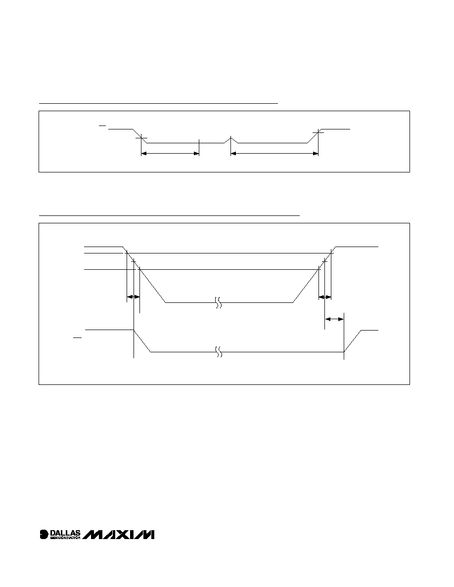
Pushbutton Reset Timing
t
RST
PB
DB
RST
Power-Switch Timing
V
CC
t
VCCF
t
VCCR
t
REC
V
PF(MAX)
V
PF
V
PF
V
PF(MIN)
RST