 | –≠–ª–µ–∫—Ç—Ä–æ–Ω–Ω—ã–π –∫–æ–º–ø–æ–Ω–µ–Ω—Ç: DS3254 | –°–∫–∞—á–∞—Ç—å:  PDF PDF  ZIP ZIP |

1 of 71
REV: 061705
Note: Some revisions of this device may incorporate deviations from published specifications known as errata. Multiple revisions of any device
may be simultaneously available through various sales channels. For information about device errata, click here:
www.maxim-ic.com/errata
.
GENERAL DESCRIPTION
The DS3251 (single), DS3252 (dual), DS3253
(triple), and DS3254 (quad) line interface units (LIUs)
perform the functions necessary for interfacing at the
physical layer to DS3, E3, or STS-1 lines. Each LIU
has independent receive and transmit paths and a
built-in jitter attenuator. An on-chip clock adapter
generates all line-rate clocks from a single input
clock. Control interface options include 8-bit parallel,
SPI, and hardware mode.
APPLICATIONS
SONET/SDH and PDH Multiplexers
Digital Cross-Connects
Access Concentrators
ATM and Frame Relay Equipment
Routers
PBXs
DSLAMs
CSU/DSUs
FUNCTIONAL DIAGRAM
FEATURES
ß
Pin-Compatible Family of Products
ß
Each Port Independently Configurable
ß
Receive Clock and Data Recovery for Up to 380
meters (DS3), 440 meters (E3), or 360 meters
(STS-1) of 75
W Coaxial Cable
ß
Standards-Compliant Transmit Waveshaping
ß
Three Control Interface Options: 8-Bit Parallel,
SPI, and Hardware Mode
ß
Built-In Jitter Attenuators can be Placed in Either
the Receive or Transmit Paths
ß
Jitter Attenuators Have Provisionable Buffer
Depth: 16, 32, 64, or 128 Bits
ß
Built-In Clock Adapter Generates All Line-Rate
Clocks from a Single Input Clock (DS3, E3,
STS-1, OC-3, 19.44MHz, 38.88MHz,
77.76MHz)
ß
B3ZS/HDB3 Encoding and Decoding
ß
Minimal External Components Required
ß
Local and Remote Loopbacks
ß
Low-Power 3.3V Operation (5V Tolerant I/O)
ß
Industrial Temperature Range: -40∞C to +85∞C
ß
Small Package: 144-Pin, 13mm x 13mm
Thermally Enhanced CSBGA
ß
Drop-In Replacement for DS3151/52/53/54 LIUs
ß
IEEE 1149.1 JTAG Support
Features continued on page 5.
ORDERING INFORMATION
PART LIU
TEMP
RANGE
PIN-PACKAGE
DS3251
1
0∞C to +70∞C
144 TE-CSBGA
DS3251N
1
-40∞C to +85∞C 144 TE-CSBGA
DS3252
2
0∞C to +70∞C
144 TE-CSBGA
DS3252N
2
-40∞C to +85∞C 144 TE-CSBGA
DS3253
3
0∞C to +70∞C
144 TE-CSBGA
DS3253N
3
-40∞C to +85∞C 144 TE-CSBGA
DS3254
4
0∞C to +70∞C
144 TE-CSBGA
DS3254N
4
-40∞C to +85∞C 144 TE-CSBGA
RXP
RXN
TXP
TXN
CLK
DATA
CLK
DATA
LINE IN
DS3, E3,
OR STS-1
LINE OUT
DS3, E3,
OR STS-1
RECEIVE
CLOCK
AND DATA
TRANSMIT
CLOCK
AND DATA
EACH LIU
STATUS
CONTROL
Dallas
Semiconductor
DS325x
DS3251/DS3252/DS3253/DS3254
Single/Dual/Triple/Quad
DS3/E3/STS-1 LIUs
www.maxim-ic.com

DS3251/DS3252/DS3253/DS3254
2 of 71
TABLE OF CONTENTS
1.
STANDARDS COMPLIANCE ......................................................................................................... 6
2.
DETAILED DESCRIPTION ............................................................................................................. 7
3.
APPLICATION EXAMPLE .............................................................................................................. 7
4.
BLOCK DIAGRAMS........................................................................................................................ 8
5.
CONTROL INTERFACE MODES.................................................................................................... 9
6.
PIN DESCRIPTIONS..................................................................................................................... 10
7.
REGISTER DESCRIPTIONS......................................................................................................... 15
8.
RECEIVER .................................................................................................................................... 24
8.1
I
NTERFACING TO THE
L
INE
........................................................................................................................... 24
8.2
O
PTIONAL
P
REAMP
..................................................................................................................................... 24
8.3
A
UTOMATIC
G
AIN
C
ONTROL
(AGC)
AND
A
DAPTIVE
E
QUALIZER
..................................................................... 24
8.4
C
LOCK AND
D
ATA
R
ECOVERY
(CDR)........................................................................................................... 24
8.5
L
OSS
-
OF
-S
IGNAL
(LOS) D
ETECTOR
............................................................................................................ 24
8.6
F
RAMER
I
NTERFACE
F
ORMAT AND THE
B3ZS/HDB3 D
ECODER
.................................................................... 25
8.7
R
ECEIVE
L
INE
-C
ODE
V
IOLATION
C
OUNTER
.................................................................................................. 26
8.8
R
ECEIVER
P
OWER
-D
OWN
........................................................................................................................... 26
8.9
R
ECEIVER
J
ITTER
T
OLERANCE
.................................................................................................................... 26
9.
TRANSMITTER ............................................................................................................................. 27
9.1
T
RANSMIT
C
LOCK
....................................................................................................................................... 27
9.2
F
RAMER
I
NTERFACE
F
ORMAT AND THE
B3ZS/HDB3 E
NCODER
.................................................................... 27
9.3
P
ATTERN
G
ENERATION
............................................................................................................................... 27
9.4
W
AVESHAPING
, L
INE
B
UILD
-O
UT
, L
INE
D
RIVER
............................................................................................ 28
9.5
I
NTERFACING TO THE
L
INE
........................................................................................................................... 28
9.6
T
RANSMIT
D
RIVER
M
ONITOR
....................................................................................................................... 28
9.7
T
RANSMITTER
P
OWER
-D
OWN
...................................................................................................................... 28
9.8
T
RANSMITTER
J
ITTER
G
ENERATION
(I
NTRINSIC
) ........................................................................................... 28
9.9
T
RANSMITTER
J
ITTER
T
RANSFER
................................................................................................................. 28
10.
JITTER ATTENUATOR ............................................................................................................. 32
11.
DIAGNOSTICS.......................................................................................................................... 34
11.1
PRBS G
ENERATOR AND
D
ETECTOR
............................................................................................................ 34
11.2
L
OOPBACKS
............................................................................................................................................... 34
12.
CLOCK ADAPTER.................................................................................................................... 35
13.
RESET LOGIC .......................................................................................................................... 35
14.
TRANSFORMERS..................................................................................................................... 36
15.
CPU INTERFACES ................................................................................................................... 37
15.1
P
ARALLEL
I
NTERFACE
................................................................................................................................. 37
15.2
SPI I
NTERFACE
.......................................................................................................................................... 37
16.
JTAG TEST ACCESS PORT AND BOUNDARY SCAN............................................................ 40
16.1
JTAG D
ESCRIPTION
................................................................................................................................... 40
16.2
JTAG TAP C
ONTROLLER
S
TATE
M
ACHINE
D
ESCRIPTION
............................................................................. 40
16.3
JTAG I
NSTRUCTION
R
EGISTER AND
I
NSTRUCTIONS
...................................................................................... 42
16.4
JTAG T
EST
R
EGISTERS
.............................................................................................................................. 43
17.
ELECTRICAL CHARACTERISTICS ......................................................................................... 44
18.
PIN ASSIGNMENTS.................................................................................................................. 56
19.
PACKAGE INFORMATION....................................................................................................... 70
20.
THERMAL INFORMATION ....................................................................................................... 71
21.
REVISION HISTORY................................................................................................................. 71

DS3251/DS3252/DS3253/DS3254
3 of 71
LIST OF FIGURES
Figure 2-1. External Connections ................................................................................................................................ 7
Figure 3-1. 4-Port Unchannelized DS3/E3 Card ......................................................................................................... 7
Figure 4-1. CPU Bus Mode Block Diagram ................................................................................................................. 8
Figure 4-2. Hardware Mode Block Diagram ................................................................................................................ 9
Figure 7-1. Status Register Logic .............................................................................................................................. 16
Figure 8-1. Receiver Jitter Tolerance ........................................................................................................................ 27
Figure 9-1. E3 Waveform Template........................................................................................................................... 30
Figure 9-2. DS3 AIS Structure ................................................................................................................................... 31
Figure 10-1. Jitter Attenuation/Jitter Transfer ............................................................................................................ 33
Figure 11-1. PRBS Output with Normal RCLK Operation ......................................................................................... 34
Figure 11-2. PRBS Output with Inverted RCLK Operation........................................................................................ 34
Figure 15-1. SPI Clock Polarity and Phase Options.................................................................................................. 38
Figure 15-2. SPI Bus Transactions............................................................................................................................ 39
Figure 16-1. JTAG Block Diagram............................................................................................................................. 41
Figure 16-2. JTAG TAP Controller State Machine .................................................................................................... 42
Figure 17-1. Transmitter Framer Interface Timing Diagram...................................................................................... 46
Figure 17-2. Receiver Framer Interface Timing Diagram .......................................................................................... 46
Figure 17-3. Parallel CPU Interface Timing Diagram (Nonmultiplexed).................................................................... 50
Figure 17-4. Parallel CPU Interface Timing Diagram (Multiplexed) .......................................................................... 52
Figure 17-5. SPI Interface Timing Diagram ............................................................................................................... 54
Figure 17-6. JTAG Timing Diagram........................................................................................................................... 55
Figure 18-1. DS3251 Hardware Mode Pin Assignment............................................................................................. 58
Figure 18-2. DS3251 Parallel Bus Mode Pin Assignment......................................................................................... 59
Figure 18-3. DS3251 SPI Bus Mode Pin Assignment ............................................................................................... 60
Figure 18-4. DS3252 Hardware Mode Pin Assignment............................................................................................. 61
Figure 18-5. DS3252 Parallel Bus Mode Pin Assignment......................................................................................... 62
Figure 18-6. DS3252 SPI Bus Mode Pin Assignment ............................................................................................... 63
Figure 18-7. DS3253 Hardware Mode Pin Assignment............................................................................................. 64
Figure 18-8. DS3253 Parallel Bus Mode Pin Assignment......................................................................................... 65
Figure 18-9. DS3253 SPI Bus Mode Pin Assignment ............................................................................................... 66
Figure 18-10. DS3254 Hardware Mode Pin Assignment........................................................................................... 67
Figure 18-11. DS3254 Parallel Bus Mode Pin Assignment....................................................................................... 68
Figure 18-12. DS3254 SPI Bus Mode Pin Assignment ............................................................................................. 69

DS3251/DS3252/DS3253/DS3254
4 of 71
LIST OF TABLES
Table 1-A. Applicable Telecommunications Standards ............................................................................................... 6
Table 6-A. Global Pin Descriptions............................................................................................................................ 10
Table 6-B. Receiver Pin Descriptions ........................................................................................................................ 11
Table 6-C. Transmitter Pin Descriptions.................................................................................................................... 11
Table 6-D. Hardware Mode Pin Descriptions ............................................................................................................ 12
Table 6-E. Parallel Bus Mode Pin Descriptions......................................................................................................... 13
Table 6-F. SPI Bus Mode Pin Descriptions ............................................................................................................... 13
Table 6-G. Transmitter Data Select Options ............................................................................................................. 14
Table 6-H. Receiver PRBS Pattern Select Options................................................................................................... 14
Table 6-I. Hardware Mode Jitter Attenuator Configuration ........................................................................................ 14
Table 7-A. Register Map............................................................................................................................................ 15
Table 9-A. DS3 Waveform Template......................................................................................................................... 29
Table 9-B. DS3 Waveform Test Parameters and Limits............................................................................................ 29
Table 9-C. STS-1 Waveform Template ..................................................................................................................... 29
Table 9-D. STS-1 Waveform Test Parameters and Limits ........................................................................................ 29
Table 9-E. E3 Waveform Test Parameters and Limits .............................................................................................. 30
Table 14-A. Transformer Characteristics................................................................................................................... 36
Table 14-B. Recommended Transformers ................................................................................................................ 36
Table 16-A. JTAG Instruction Codes ......................................................................................................................... 42
Table 16-B. JTAG ID Code........................................................................................................................................ 43
Table 17-A. Recommended DC Operating Conditions.............................................................................................. 44
Table 17-B. DC Characteristics ................................................................................................................................. 44
Table 17-C. Framer Interface Timing......................................................................................................................... 45
Table 17-D. Receiver Input Characteristics--DS3 and STS-1 Modes ...................................................................... 47
Table 17-E. Receiver Input Characteristics--E3 Mode ............................................................................................. 47
Table 17-F. Transmitter Output Characteristics--DS3 and STS-1 Modes................................................................ 48
Table 17-G. Transmitter Output Characteristics--E3 Mode...................................................................................... 48
Table 17-H. Parallel CPU Interface Timing ............................................................................................................... 49
Table 17-I. SPI Interface Timing ................................................................................................................................ 54
Table 17-J. JTAG Interface Timing............................................................................................................................ 55
Table 18-A. Pin Assignments Sorted by Signal Name .............................................................................................. 56
Table 20-A. Thermal Properties, Natural Convection................................................................................................ 71
Table 20-B. Theta-JA (
q
JA
) vs. Airflow ....................................................................................................................... 71

DS3251/DS3252/DS3253/DS3254
5 of 71
FEATURES (CONTINUED)
Receiver
ß
AGC/equalizer block handles from 0 to 15dB of cable loss
ß
Loss-of-lock (LOL) PLL status indication
ß
Interfaces directly to a DSX monitor signal (~20dB flat loss) using built-in preamp
ß
Digital and analog loss-of-signal (LOS) detectors (ANSI T1.231 and ITU G.775)
ß
Optional B3ZS/HDB3 decoder
ß
Line-code violation output pin and counter
ß
Binary or bipolar framer interface
ß
On-board 2
15
- 1 and 2
23
- 1 PRBS detector
ß
Clock inversion for glueless interfacing
ß
Tri-state clock and data outputs support protection switching applications
ß
Per-channel power-down control
Transmitter
ß
Binary or bipolar framer interface
ß
Gapped clock capable up to 51.84MHz
ß
Wide 50
± 20% transmit clock duty cycle
ß
Clock inversion for glueless interfacing
ß
Optional B3ZS/HDB3 encoder
ß
On-board 2
15
- 1 and 2
23
- 1 PRBS generator
ß
Complete DS3 AIS generator (ANSI T1.107)
ß
Unframed all-ones generator (E3 AIS)
ß
Line build-out (LBO) control
ß
Tri-state line driver outputs support protection switching applications
ß
Per-channel power-down control
ß
Output driver monitor
Jitter Attenuator
ß
On-chip crystal-less jitter attenuator
ß
Meets all applicable ANSI, ITU, ETSI and Telcordia jitter transfer and output jitter requirements
ß
Can be placed in the transmit path, receive path or disabled
ß
Selectable FIFO depth: 16, 32, 64 or 128 bits
ß
Overflow and underflow status indications
Clock Adapter
ß
Operates from a single DS3, E3, STS-1, 19.44 MHz, 38.88 MHz, or 77.76 MHz master clock
ß
Synthesizes clock rates that are not provided externally
ß
Use of common system timing frequencies such as 19.44 MHz eliminates the need for any local oscillators,
reduces cost and board space
ß
Very small jitter gain and intrinsic jitter generation
ß
Optionally provides synthesized clocks on output pins for use by neighboring components, such as framers or
mappers
Parallel CPU Interface
ß
Multiplexed or nonmultiplexed 8-bit interface
ß
Configurable for Intel mode (
CS, WR, RD) or Motorola mode (CS, DS, R/W)
SPI CPU Interface
ß
Operation up to 10 Mbit/s
ß
Burst mode for multi-byte read and write accesses
ß
Programmable clock polarity and phase
ß
Half-duplex operation gives option to tie SDI and SDO together externally to reduce wire count

DS3251/DS3252/DS3253/DS3254
6 of 71
1. STANDARDS COMPLIANCE
Table 1-A. Applicable Telecommunications Standards
SPECIFICATION SPECIFICATION
TITLE
ANSI
T1.102-1993
Digital Hierarchy--Electrical Interfaces
T1.107-1995
Digital Hierarchy--Formats Specification
T1.231-1997
Digital Hierarchy--Layer 1 In-Service Digital Transmission Performance Monitoring
T1.404-1994
Network-to-Customer Installation--DS3 Metallic Interface Specification
ITU-T
G.703
Physical/Electrical Characteristics of Hierarchical Digital Interfaces, 1991
G.751
Digital Multiplex Equipment Operating at the Third-Order Bit Rate of 34,368kbps and the
Fourth-Order Bit Rate of 139,264kbps and Using Positive Justification, 1993
G.775
Loss of Signal (LOS) and Alarm Indication Signal (AIS) Defect Detection and Clearance
Criteria, November 1994
G.823
The Control of Jitter and Wander within Digital Networks that are Based on the 2048kbps
Hierarchy, 1993
G.824
The Control of Jitter and Wander within Digital Networks that are Based on the 1544kbps
Hierarchy, 1993
O.151
Error Performance Measuring Equipment Operating at the Primary Rate and Above,
October 1992
ETSI
ETS 300 686
Business TeleCommunications; 34Mbps and 140Mbps Digital Leased Lines (D34U,
D34S, D140U, and D140S); Network Interface Presentation, 1996
ETS 300 687
Business TeleCommunications; 34Mbps Digital Leased Lines (D34U and D34S);
Connection Characteristics, 1996
ETS EN 300 689
Access and Terminals (AT); 34Mbps Digital Leased Lines (D34U and D34S); Terminal
equipment interface, July 2001
TBR 24
Business TeleCommunications; 34Mbps Digital Unstructured and Structured Lease Lines;
Attachment Requirements for Terminal Equipment Interface, 1997
TELCORDIA
GR-253-CORE
SONET Transport Systems: Common Generic Criteria, Issue 2, December 1995
GR-499-CORE
Transport Systems Generic Requirements (TSGR): Common Requirements, Issue 1,
December 1998

DS3251/DS3252/DS3253/DS3254
7 of 71
2. DETAILED DESCRIPTION
The DS3251 (single), DS3252 (dual), DS3253 (triple), and DS3254 (quad) LIUs perform the functions necessary
for interfacing at the physical layer to DS3, E3, or STS-1 lines. Each LIU has independent receive and transmit
paths and a built-in jitter attenuator. The receiver performs clock and data recovery from a B3ZS- or HDB3-coded
alternate mark inversion (AMI) signal and monitors for loss of the incoming signal. The receiver optionally performs
B3ZS/HDB3 decoding and outputs the recovered data in either binary or bipolar format. The transmitter accepts
data in either binary or bipolar format, optionally performs B3ZS/HDB3 encoding, and drives standard pulse-shape
waveforms onto 75
W coaxial cable. The jitter attenuator can be mapped into the receiver data path, mapped into
the transmitter data path, or be disabled. An on-chip clock adapter generates all line-rate clocks from a single input
clock. Control interface options include 8-bit parallel, SPI
TM
, and hardware mode. The DS325x LIUs conform to the
telecommunications standards listed in
Table 1-A
.
Figure 2-1
shows the external components required for proper
operation.
Shorthand Notations. The notation "DS325x" throughout this data sheet refers to either the DS3251, DS3252,
DS3253, or DS3254. This data sheet is the specification for all four devices. The LIUs on the DS325x devices are
identical. For brevity, this document uses the pin name and register name shorthand "NAMEn," where "n" stands in
place of the LIU port number. For example, on the DS3254 quad LIU, TCLKn is shorthand notation for pins TCLK1,
TCLK2, TCLK3, and TCLK4 on LIU ports 1, 2, 3, and 4, respectively. This document also uses generic pin and
register names such as TCLK (without a number suffix) when describing LIU operation. When working with a
specific LIU on the DS325x devices, generic names like TCLK should be converted to actual pin names, such as
TCLK1.
Figure 2-1. External Connections
3. APPLICATION EXAMPLE
Figure 3-1. 4-Port Unchannelized DS3/E3 Card
SPI is a trademark of Motorola, Inc.
DS3144
QUAD
DS3/E3
FRAMER
BAC
K
PL
AN
E
DS3254
QUAD
DS3/E3/STS-1
LIU
1:2ct
1:2ct
0.05
mF
(optional)
TRANSMIT
RECEIVE
TXP
TXN
RXP
RXN
0.01
mF
3.3V
POWER
PLANE
GROUND
PLANE
V
DD
EACH LIU
0.1
mF
1
mF
330
W
(1%)
330
W
(1%)
0.01
mF
0.1
mF
1
mF
0.01
mF
0.1
mF
1
mF
V
DD
V
DD
V
SS
V
SS
V
SS
Dallas
Semiconductor
DS325x
0.05
mF
(optional)
DS3251/DS3252/DS3253/DS3254
8 of 71
4. BLOCK DIAGRAMS
Figure 4-1. CPU Bus Mode Block Diagram
Dallas
Semiconductor
DS325x
CPU Bus I/O
(see detailed
views below)
HW = 0
HIZ
MOT
CS
WR / R/W
RD / DS
A[5:0]
D[7:0]
INT
ALE
RST
CPU Bus
Interface
and
Global
Configuration
PARALLEL INTERFACE
HW = 0
HIZ
INT
RST
CPU Bus
Interface
and
Global
Configuration
SPI INTERFACE
CS
SCLK
SDI
SDO
CPHA
CPOL
MOT=0,
WR=0, RD=0
TTSn
PRBSn
TCLKn
TNEGn
RCLKn
RTSn
Analog
Local
Loopback
P
r
eamp
Clock &
Data
Recovery
L
i
n
e
Dr
ive
r
W
a
veshapi
ng
Clock
Invert
RXPn
RXNn
TXPn
TXNn
RLOSn
Power
Supply
B3ZS/
HDB3
Encoder
Mux
Mux
PRBS
Detector
B3ZS/HDB3
Decoder
Digital LOS
Detector
squelch
Jitter A
ttenuat
or
(can be
pl
aced i
n
ei
t
h
er t
h
e rec
e
i
v
e path
or t
h
e transmi
t
path
)
Driver
Monitor
Loopback Control
TDMn
VDD
VSS
Remote
Loopback
CPU Bus
Interface
and
Global
Configuration
Output
Drivers,
Clock
Invert
Digital
Local
Loopback
Automatic
Gain
Control
+
Adaptive
Equalizer
ALOS
STMCLK
Clock
Adapter
E3MCLK
T3MCLK
TPOSn/TDATn
RNEGn/RLCVn
RPOSn/RDATn
AIS, 100100...,
PRBS Pattern
Generation
Mux
TCLKn
master clock

DS3251/DS3252/DS3253/DS3254
9 of 71
Figure 4-2. Hardware Mode Block Diagram
5. CONTROL INTERFACE MODES
The DS325x devices can operate in hardware mode or two different CPU bus modes: 8-bit parallel and SPI serial.
In hardware mode, configuration input pins control device configuration, while status output pins indicate device
status. Internal registers are not accessible in hardware mode. The device is configured for hardware mode when
the HW pin is wired high (HW = 1).
In the CPU bus modes, most of the configuration and status pins used in hardware mode are reassigned to the
CPU bus interface. Through the bus interface an external processor can access a set of internal configuration and
status registers. A few configuration and status pins are active in both hardware mode and the CPU bus modes to
support specialized applications, such as protection switching. The device is configured for CPU bus mode when
the HW pin is wired low (HW = 0). The default CPU interface is 8-bit parallel. When the MOT,
RD and WR pins are
all low, the SPI interface is enabled. See Section
15
for more information on the CPU interfaces.
With the exception of the HW pin, configuration and status pins available in hardware mode have corresponding
register bits in the CPU bus mode. The hardware mode pins and the CPU bus mode register bits have identical
names and functions, with the exception that all register bits are active high. For example, LOS is indicated by the
receiver on the
RLOS pin (active low) in hardware mode and the RLOS register bit (active high) in CPU bus mode.
The few configuration input pins that are active in CPU bus mode also have corresponding register bits. In these
cases, the actual configuration is the logical OR of pin assertion and register bit assertion. For example, the
transmitter output driver is tri-stated if the
TTS pin is asserted (i.e., low) or the TTS register bit is asserted (high).
Figure 4-1
and
Figure 4-2
show block diagrams of the DS325x in hardware mode and in CPU bus mode.
Analog
Local
Loopback
P
r
eamp
Automatic
Gain
Control
+
Adaptive
Equalizer
ALOS
Clock &
Data
Recovery
Li
ne D
r
i
v
er
Waveshaping
Clock
Invert
RXPn
RXNn
TXPn
TXNn
TTSn
PRBSn
TLBOn
TCINV
TPOSn/TDATn
TCLKn
TNEGn
E3Mn
RNEGn/RLCVn
RCLKn
RPOSn/RDATn
RLOSn
RMONn
Power
Supply
TDSAn,
TDSBn
B3ZS/
HDB3
Encoder
AIS, 100100...,
PRBS Pattern
Generation
Mux
Mux
Mux
PRBS
Detector
B3ZS/HDB3
Decoder
Digital LOS
Detector
squelch
Jitter A
ttenuat
or
(can be
pl
aced i
n
ei
t
h
er t
h
e rec
e
i
v
e path
or t
h
e transmi
t
path
)
Driver
Monitor
Loopback Control
TDMn
LLBn
VDD
VSS
TJAn
TBIN
RCINV
Remote
Loopback
Global
Configuration
STSn
Output
Drivers,
Clock
Invert
RTSn
RBIN
RJAn
HW
HIZ
Digital
Local
Loopback
RLBn
RST
Clock
Adapter
T3MCLK
E3MCLK
STMCLK
TCLKn
master clock
Dallas
Semiconductor
DS325x
DS3251/DS3252/DS3253/DS3254
10 of 71
6. PIN DESCRIPTIONS
Table 6-A
through
Table 6-C
list the pins that are always active.
Table 6-D
through
Table 6-F
list the additional pins
that active in each of the three control interface modes. Section
18
shows pin assignments for all three control
interface modes.
Table 6-A. Global Pin Descriptions
Note: These pins are always active.
NAME
TYPE
FUNCTION
T3MCLK I/O
T3 Master Clock. If a clock is applied to T3MCLK, it must be transmission-quality (
±20ppm, low jitter).
When present, the T3MCLK signal serves as the DS3 master clock for the CDRs and jitter attenuators
of all LIUs configured for DS3 operation. If T3MCLK is held low, the clock adapter block synthesizes the
DS3 master clock from the clock applied to E3MCLK (first choice) or the clock applied to STMCLK
(second choice). If T3MCLK is held high, each LIU in DS3 mode uses its TCLK signal as its master
clock. If T3MCLK is held low but E3MCLK and STMCLK are not toggling, then each LIU in DS3 mode
uses its TCLK signal as its master clock. Pin is input-only in Hardware mode, input/output in CPU Bus
mode. See Section
12
for more information.
E3MCLK I/O
E3 Master Clock. If a clock is applied to E3MCLK, it must be transmission-quality (
±20ppm, low jitter).
When present, the E3MCLK signal serves as the E3 master clock for the CDRs and jitter attenuators of
all LIUs configured for E3 operation. If E3MCLK is held low, the clock adapter block synthesizes the E3
master clock from the clock applied to T3MCLK (first choice) or the clock applied to STMCLK (second
choice). If E3MCLK is held high, each LIU in E3 mode uses its TCLK signal as its master clock. If
E3MCLK is held low but T3MCLK and STMCLK are not toggling, then each LIU in E3 mode uses its
TCLK signal as its master clock. Pin is input-only in Hardware mode, input/output in CPU Bus mode.
See Section
12
for more information.
STMCLK I/O
STS-1 Master Clock. If a clock is applied to STMCLK, it must be transmission-quality (
±20ppm, low
jitter). When present, the STMCLK signal serves as the STS-1 master clock for the CDRs and jitter
attenuators of all LIUs configured for STS-1 operation. If STMCLK is held low, the clock adapter block
synthesizes the STS-1 master clock from the clock applied to T3MCLK (first choice) or the clock
applied to E3MCLK (second choice). If STMCLK is held high, each LIU in STS-1 mode uses its TCLK
signal as its master clock. If STMCLK is held low but T3MCLK and E3MCLK are not toggling, then each
LIU in STS-1 mode uses its TCLK signal as its master clock. Pin is input-only in Hardware mode,
input/output in CPU Bus mode. See Section
12
for more information.
HIZ
I
PU
High-Z Enable Input (Active Low, Open Drain, Internal 10k
W Pullup to V
DD
)
0 = tri-state all output pins (Note that the
JTRST pin must be low.)
1 = normal operation
HW I
Hardware Mode Select
0 = CPU bus mode
1 = Hardware mode
See Section
5
for details.
JTCLK I
JTAG IEEE 1149.1 Test Serial Clock. JTCLK shifts data into JTDI on the rising edge and out of JTDO
on the falling edge. If boundary scan is not used, JTCLK should be pulled high.
JTDI I
PU
JTAG IEEE 1149.1 Test Serial-Data Input (Internal 10k
W Pullup). Test instructions and data are
clocked in on this pin on the rising edge of JTCLK. If boundary scan is not used, JTDI should be left
unconnected or pulled high.
JTDO O
JTAG IEEE 1149.1 Test Serial-Data Output. Test instructions and data are clocked out on this pin on
the falling edge of JTCLK.
JTRST
I
PU
JTAG IEEE 1149.1 Test Reset (Internal 10k
W Pullup to V
DD
). This pin is used to asynchronously
reset the test access port (TAP) controller. If boundary scan is not used,
JTRST can be held low or
high.
JTMS I
PU
JTAG IEEE 1149.1 Test Mode Select (Internal 10k
W Pullup to V
DD
). This pin is sampled on the rising
edge of JTCLK and is used to place the port into the various defined IEEE 1149.1 states. If boundary
scan is not used, JTMS should be left unconnected or pulled high.
RST
I
PU
Reset Input (Active Low, Open Drain, Internal 10k
W Pullup to V
DD
). When this global asynchronous
reset is pulled low, the internal circuitry is reset and the internal registers (CPU bus mode) are forced to
their default values. The device is held in reset as long as
RST is low. RST should be held low for at
least two master clock cycles. See Section
13
for more information.
TEST
I
PU
Factory Test Pin. Leave unconnected or wire high for normal operation.
V
DD
P
Positive Supply. 3.3V
±5%. All V
DD
signals should be wired together.
V
SS
P
Ground Reference. All V
SS
signals should be wired together.
DS3251/DS3252/DS3253/DS3254
11 of 71
Table 6-B. Receiver Pin Descriptions
Note: These pins are always active.
NAME
TYPE
FUNCTION
RXPn,
RXNn
I
Receiver Analog Inputs. These differential AMI inputs are coupled to the inbound 75
W coaxial cable
through a 1:2 step-up transformer (
Figure 2-1
).
RCLKn O3
Receiver Clock. The recovered clock is output on the RCLK pin. Recovered data is output on the
RPOS/RDAT and RNEG/RLCV pins on the falling edge of RCLK (RCINV = 0) or the rising edge of
RCLK (RCINV = 1). During a loss of signal (
RLOS = 0), the RCLK output signal is derived from the
LIU's master clock.
RPOSn/
RDATn
O3
Receiver Positive AMI/Receiver Data. When the receiver is configured to have a bipolar interface
(RBIN = 0), RPOS pulses high for each positive AMI pulse received. When the receiver is configured
to have a binary interface (RBIN = 1), RDAT outputs decoded binary data. RPOS/RDAT is updated
either on the falling edge of RCLK (RCINV = 0) or the rising edge of RCLK (RCINV = 1).
RNEGn/
RLCVn
O3
Receiver Negative AMI/Line-Code Violation. When the receiver is configured to have a bipolar
interface (RBIN = 0), RNEG pulses high for each negative AMI pulse received. When the receiver is
configured to have a binary interface (RBIN = 1), RLCV pulses high to flag code violations. See
Section
8.6
for further details on code violations. RNEG/RLCV is updated either on the falling edge of
RCLK (RCINV = 0) or the rising edge of RCLK (RCINV = 1).
RTSn
I
Receiver Tri-State Enable (Active Low).
RTS tri-states the RPOS/RDAT, RNEG/RLCV, and RCLK
receiver outputs. This feature supports applications requiring LIU redundancy. Receiver outputs from
multiple LIUs can be wire-ORed together, eliminating the need for external switches or muxes. The
receiver continues to operate internally when
RTS is low.
0 = tri-state the receiver outputs
1 = enable the receiver outputs
RLOSn
O
Receiver Loss of Signal (Active Low, Open Drain).
RLOS is asserted upon detection of 175 ±75
consecutive zeros in the receive data stream.
RLOS is deasserted when there are no excessive zero
occurrences over a span of 175
±75 clock periods. An excessive zero occurrence is defined as three
or more consecutive zeros in the DS3 and STS-1 modes or four or more zeros in the E3 mode. See
Section
8.5
for more information.
PRBSn O
PRBS Detector Output. This signal reports the status of the PRBS detector. See Section
11
for
further details.
Table 6-C. Transmitter Pin Descriptions
Note: These pins are always active.
NAME
TYPE
FUNCTION
TCLKn I
Transmitter Clock. A DS3 (44.736MHz
±20ppm), E3 (34.368MHz ±20ppm), or STS-1 (51.840MHz
±20ppm) clock should be applied at this signal. Data to be transmitted is clocked into the device at
TPOS/TDAT and TNEG either on the rising edge of TCLK (TCINV = 0) or the falling edge of TCLK
(TCINV = 1). See Section
9
for additional details.
TPOSn/
TDATn
I
Transmitter Positive AMI/Transmitter Data. When the transmitter is configured to have a bipolar
interface (TBIN = 0), a positive pulse is transmitted on the line when TPOS is high. When the
transmitter is configured to have a binary interface (TBIN = 1), the data on TDAT is transmitted after
B3ZS or HDB3 encoding. TPOS/TDAT is sampled either on the rising edge of TCLK (TCINV = 0) or
on the falling edge of TCLK (TCINV = 1).
TNEGn I
Transmitter Negative AMI. When the transmitter is configured to have a bipolar interface (TBIN = 0),
a negative pulse is transmitted on the line when TNEG is high. When the transmitter is configured to
have a binary interface (TBIN = 1), TNEG is ignored and should be wired either high or low. TNEG is
sampled either on the rising edge of TCLK (TCINV = 0) or on the falling edge of TCLK (TCINV = 1).
TXPn,
TXNn
O3
Transmitter Analog Outputs. These differential AMI outputs are coupled to the outbound 75
W
coaxial cable through a 2:1 step-down transformer (
Figure 2-1
). These outputs can be tri-stated using
the
TTS pin or the TTS or TPS configuration bits.
TDMn
O
Transmitter Driver Monitor (Active Low, Open Drain).
TDM reports the status of the transmit driver
monitor. When the monitor detects a faulty transmitter,
TDM is driven low. TDM requires an external
pullup to V
DD
. See Section
9.6
for more information.
TTSn
I
Transmitter Tri-State Enable (Active Low).
TTS tri-states the transmitter outputs (TXP and TXN).
This feature supports applications requiring LIU redundancy. Transmitter outputs from multiple LIUs
can be wire-ORed together, eliminating external switches. The transmitter continues to operate
internally when
TTS is active.
0 = tri-state the transmitter output driver
1 = enable the transmitter output driver

DS3251/DS3252/DS3253/DS3254
12 of 71
Table 6-D. Hardware Mode Pin Descriptions
Note: These pins are active in hardware mode.
NAME
TYPE
FUNCTION
E3Mn I
E3 Mode Enable
0 = DS3 operation
1 = E3 or STS-1 operation
STSn I
STS-1 Mode Enable
When E3M = 1,
0 = E3 operation
1 = STS-1 operation
When E3M = 0, STS selects the DS3 AIS pattern. See
Table 6-G
.
LLBn,
RLBn
I
Local Loopback Select, Remote Loopback Select
{LLB, RLB} =
00 = no loopback
01 = remote loopback
10 = analog local loopback
11 = digital local loopback
RBIN I
Receiver Binary Framer-Interface Enable
0 = Receiver framer interface is bipolar on the RPOS and RNEG pins. The B3ZS/HDB3 decoder is
disabled.
1 = Receiver framer interface is binary on the RDAT pin with the RLCV pin indicating line-code
violations. The B3ZS/HDB3 encoder is enabled.
RCINV I
Receiver Clock Invert
0 = RPOS/RDAT and RNEG/RLCV update on the falling edge of RCLK.
1 = RPOS/RDAT and RNEG/RLCV update on the rising edge of RCLK.
RJAn I
Receiver Jitter Attenuator Enable
0 = remove jitter attenuator from the receiver path
1 = insert jitter attenuator into the receiver path
See
Table 6-I
for more information.
RMONn I
Receive Monitor-Preamp Enable. RMON determines whether or not the receiver's preamp is enabled
to provide flat gain to the incoming signal before the AGC/equalizer block processes it. This feature
should be enabled when the device is being used to monitor signals that have been resistively
attenuated by a monitor jack. See Section
8.2
for more information.
0 = disable the monitor preamp
1 = enable the monitor preamp
TBIN I
Transmitter Binary Framer-Interface Enable
0 = Transmitter framer interface is bipolar on the TPOS and TNEG pins. The B3ZS/HDB3 encoder is
disabled.
1 = Transmitter framer interface is binary on the TDAT pin. (TNEG is ignored and should be wired low.)
The B3ZS/HDB3 encoder is enabled.
TCINV I
Transmitter Clock Invert
0 = TPOS/TDAT and TNEG are sampled on the rising edge of TCLK.
1 = TPOS/TDAT and TNEG are sampled on the falling edge of TCLK.
TDSAn,
TDSBn
I
Transmitter Data Select. These inputs select the source of the transmit data. See
Table 6-G
for
details.
TJAn I
Transmitter Jitter Attenuator Enable
0 = remove jitter attenuator from the transmitter path
1 = insert jitter attenuator into the transmitter path
See
Table 6-I
for more information.
TLBOn I
Transmitter Line Build-Out Enable. TLBO indicates cable length for waveform shaping in DS3 and
STS-1 modes. TLBO is ignored for E3 mode and should be wired high or low.
0 = cable length
≥ 225ft
1 = cable length < 225ft
DS3251/DS3252/DS3253/DS3254
13 of 71
Table 6-E. Parallel Bus Mode Pin Descriptions
Note: These pins are active in parallel bus mode.
NAME
TYPE
FUNCTION
MOT I
Motorola-Style Parallel CPU Interface
0 = Parallel CPU interface is Intel-style
1 = Parallel CPU interface is Motorola-style
ALE I
Address Latch Enable. This signal controls a latch on the A[3:0] inputs. For a nonmultiplexed parallel
CPU interface, ALE is wired high to make the latch transparent. For a multiplexed parallel CPU
interface, the falling edge of ALE latches the address.
CS
I
Chip Select (Active Low).
CS must be asserted to read or write internal registers.
WR / R/W
I
Write Enable (Active Low) or Read/Write Select. For the Intel-style parallel CPU interface (MOT =
0),
WR is asserted to write internal registers. For the Motorola-style parallel CPU interface (MOT = 1),
R/
W determines the type of bus transaction, with R/W = 1 indicating a read and R/W = 0 indicating a
write.
RD / DS
I
Read Enable (Active Low) or Data Strobe (Active Low). For the Intel-style parallel CPU interface
(MOT = 0),
RD is asserted to read internal registers. For the Motorola-style parallel CPU interface
(MOT = 1), the rising edge of
DS writes data to internal registers.
A[5:0] I
Address Bus. These inputs specify the address of the internal register to be accessed. A5 is not
present on the DS3252. A5 and A4 are not present on the DS3251.
D[7:0] I/O
Data Bus. These bidirectional lines are inputs during writes to internal registers and outputs during
reads.
INT
O
Interrupt Output (Active Low, Open Drain). This pin is forced low in response to one or more
unmasked, active interrupt sources within the device.
INT remains low until the interrupt is serviced or
masked.
Table 6-F. SPI Bus Mode Pin Descriptions
Note: These pins are active in SPI bus mode.
NAME
TYPE
FUNCTION
MOT
,
RD, WR
I
Wire these pins low to enable SPI bus mode.
CS
I
Chip Select (Active Low).
CS must be asserted to read or write internal registers.
SCLK I
Serial Clock for SPI Interface. SCLK is always driven by the SPI bus master.
SDI I
Serial Data Input for SPI Interface. The SPI bus master transmits data to the device on this pin.
SDO O
Serial Data Output for SPI Interface
The device transmits data to the SPI bus master on this pin.
CPHA I
SPI Clock Phase
0 = data is latched on the leading edge of the SCLK pulse
1 = data is latched on the trailing edge of the SCLK pulse
CPOL I
SPI Clock Polarity
0 = SCLK is normally low and pulses high during bus transactions
1 = SCLK is normally high and pulses low during bus transactions
INT
O
Interrupt Output (Active Low, Open Drain). This pin is forced low in response to one or more
unmasked, active interrupt sources within the device.
INT remains low until the interrupt is serviced or
masked.
Note 1: PIN TYPES
I = input pin
I
PU
= input pin with internal 10k
W pullup
O = output pin
O3 = output pin that can be tri-stated
P = power-supply pin

DS3251/DS3252/DS3253/DS3254
14 of 71
Table 6-G. Transmitter Data Select Options
TDSA TDSB E3M STS
Tx
MODE
TRANSMIT DATA SELECTED
0
0
X
X
Any
Normal data as input at TPOS and TNEG
0 1 0 0
DS3
0 1 1 0 E3
0 1 1 1
STS-1
Unframed all ones
0
1
0
1
DS3
DS3 AIS per ANSI T1.107 (
Figure 9-2
)
1
0
X
X
Any
Unframed 100100... pattern
1 1 1 0 E3
2
23
- 1 PRBS pattern per ITU O.151
1 1 0 X
DS3
1 1 1 1
STS-1
2
15
- 1 PRBS pattern per ITU O.151
Note 1:
This coding of the TDSA, TDSB, E3M, and STS bits allows AIS generation to be enabled by
holding TDSA = 0 and changing TDSB from 0 to 1. The type of DS3 AIS signal is selected by the
STS bit with E3M = 0.
Note 2:
If E3M and/or STS are changed when {TDSA,TDSB}
π 00, TDSA and TDSB must both be cleared
to 0. After they are cleared, TDSA and TDSB can be configured to transmit a pattern in the new
operating mode.
Table 6-H. Receiver PRBS Pattern Select Options
E3M STS
Rx
MODE
RECEIVER PRBS PATTERN
SELECTED
1 0 E3
2
23
- 1 PRBS pattern per ITU O.151
0 X
DS3
1 1
STS-1
2
15
- 1 PRBS pattern per ITU O.151
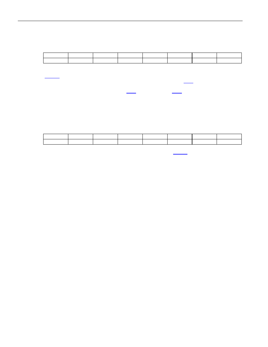
Table 6-I. Hardware Mode Jitter Attenuator Configuration
TJA
RJA
JITTER ATTENUATOR CONFIGURATION
0 0
Disabled
0
1
Receive path, 16-bit buffer depth
1
0
Transmit path, 16-bit buffer depth
1
1
Transmit path, 32-bit buffer depth
DS3251/DS3252/DS3253/DS3254
15 of 71
7. REGISTER DESCRIPTIONS
When the DS325x is configured in either of the two CPU bus modes (HW = 0), the registers shown in
Table 7-A
are accessible through the CPU bus interfaces. All registers for the LIU ports are forced to their default values
during an internal power-on reset or when the
RST pin is driven low. Setting an LIU's RST bit high forces all
registers for that LIU to their default values. All register bits marked "--" must be written 0 and ignored when read.
The TEST registers must be left at their reset value of 00h for normal operation.
On the DS3253, only registers for LIUs 1, 2, and 3 are available. Writes into LIU 4 address space are ignored.
Reads from LIU 4 address space return all zeros. On the DS3252, address line A5 is not present, limiting the
address space to the LIU 1 and LIU 2 registers. On the DS3251, address lines A5 and A4 are not present, limiting
the address space to the LIU 1 registers.
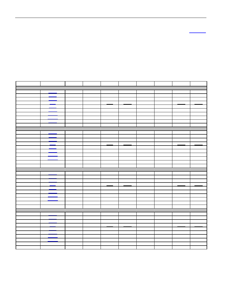
Table 7-A. Register Map
ADDRESS REGISTER BIT
7 BIT
6 BIT
5 BIT
4 BIT
3 BIT
2 BIT
1 BIT
0
LIU 1
00h
GCR1
E3M
STS
LLB
RLB
TDSA
TDSB -- RST
01h
TCR1
JAL[1]
TBIN
TCINV
TJA TPD TTS
TLBO
JAL[0]
02h
RCR1
ITU RBIN
RCINV RJA RPD RTS RMON
RCVUD
03h
SR1
--
--
TDM PRBS -- -- RLOL RLOS
04h
SRL1
JAFL
JAEL
TDML
PRBSL
PBERL
RCVL
RLOLL
RLOSL
05h
SRIE1
JAFIE
JAEIE
TDMIE
PRBSIE
PBERIE
RCVIE
RLOLIE
RLOSIE
06h
RCVL1
RCV[7] RCV[6] RCV[5] RCV[4] RCV[3] RCV[2] RCV[1] RCV[0]
07h
RCVH1
RCV[15] RCV[14] RCV[13] RCV[12] RCV[11] RCV[10] RCV[9] RCV[8]
08h
CACR
T3MOE
E3MOE
STMOE -- --
AMCSEL[1]
AMCSEL[0]
AMCEN
09h≠0Fh
Test
Registers
-- -- -- -- -- -- -- --
LIU 2
10h
GCR2
E3M
STS
LLB
RLB
TDSA
TDSB -- RST
11h
TCR2
JAL[1]
TBIN
TCINV
TJA TPD TTS
TLBO
JAL[0]
12h
RCR2
ITU RBIN
RCINV RJA RPD RTS RMON
RCVUD
13h
SR2
--
--
TDM PRBS -- -- RLOL RLOS
14h
SRL2
JAFL
JAEL
TDML
PRBSL
PBERL
RCVL
RLOLL
RLOSL
15h
SRIE2
JAFIE
JAEIE
TDMIE
PRBSIE
PBERIE
RCVIE
RLOLIE
RLOSIE
16h
RCVL2
RCV[7] RCV[6] RCV[5] RCV[4] RCV[3] RCV[2] RCV[1] RCV[0]
17h
RCVH2
RCV[15] RCV[14] RCV[13] RCV[12] RCV[11] RCV[10] RCV[9] RCV[8]
18h unused -- -- -- -- -- -- -- --
19h≠1Fh
Test
Registers
-- -- -- -- -- -- -- --
LIU 3
20h
GCR3
E3M
STS
LLB
RLB
TDSA
TDSB -- RST
21h
TCR3
JAL[1]
TBIN
TCINV
TJA TPD TTS
TLBO
JAL[0]
22h
RCR3
ITU RBIN
RCINV RJA RPD RTS RMON
RCVUD
23h
SR3
--
--
TDM PRBS -- -- RLOL RLOS
24h
SRL3
JAFL
JAEL
TDML
PRBSL
PBERL
RCVL
RLOLL
RLOSL
25h
SRIE3
JAFIE
JAEIE
TDMIE
PRBSIE
PBERIE
RCVIE
RLOLIE
RLOSIE
26h
RCVL3
RCV[7] RCV[6] RCV[5] RCV[4] RCV[3] RCV[2] RCV[1] RCV[0]
27h
RCVH3
RCV[15] RCV[14] RCV[13] RCV[12] RCV[11] RCV[10] RCV[9] RCV[8]
28h unused -- -- -- -- -- -- -- --
29h≠2Fh
Test
Registers
-- -- -- -- -- -- -- --
LIU 4
30h
GCR4
E3M
STS
LLB
RLB
TDSA
TDSB -- RST
31h
TCR4
JAL[1]
TBIN
TCINV
TJA TPD TTS
TLBO
JAL[0]
32h
RCR4
ITU RBIN
RCINV RJA RPD RTS RMON
RCVUD
33h
SR4
--
--
TDM PRBS -- -- RLOL RLOS
34h
SRL4
JAFL
JAEL
TDML
PRBSL
PBERL
RCVL
RLOLL
RLOSL
35h
SRIE4
JAFIE
JAEIE
TDMIE
PRBSIE
PBERIE
RCVIE
RLOLIE
RLOSIE
36h
RCVL4
RCV[7] RCV[6] RCV[5] RCV[4] RCV[3] RCV[2] RCV[1] RCV[0]
37h
RCVH4
RCV[15] RCV[14] RCV[13] RCV[12] RCV[11] RCV[10] RCV[9] RCV[8]
38h unused -- -- -- -- -- -- -- --
39h≠3Fh
Test
Registers
-- -- -- -- -- -- -- --
Note 1: Underlined bits are read-only; all other bits are read-write.
Note 2: The registers are named REGn, where n = the LIU number (1, 2, 3, or 4). The register names are hyperlinks to the register descriptions.
Note 3: The bit names are the same for each LIU register set.
DS3251/DS3252/DS3253/DS3254
16 of 71
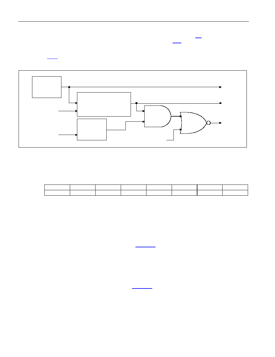
Status Register Description
The status registers have two types of status bits. Real-time status bits--located in the
SR
registers--indicate the
state of a signal at the time it was read. Latched status bits--located in the
SRL
registers--are set when a signal
changes state (low-to-high, high-to-low, or both, depending on the bit) and cleared when written with a logic 1
value. After clearing, latched status bits remain cleared until the signal changes state again. Interrupt-enable bits--
located in the
SRIE
registers--control whether or not the
INT pin is driven low when latched register bits are set.
Figure 7-1. Status Register Logic
Register Name:
GCRn
Register Description:
Global Configuration Register
Register Address:
00h, 10h, 20h, 30h
Bit
7 6 5 4 3 2 1 0
Name E3M
STS
LLB
RLB
TDSA
TDSB
--
RST
Default 0 0 0 0 0 0 -- 0
Bit 7: E3 Mode Enable (E3M)
0 = DS3 operation
1 = E3 or STS-1 operation
Bit 6: STS-1 Mode Enable (STS)
When E3M = 1,
0 = E3 operation
1 = STS-1 operation
When E3M = 0, STS selects the DS3 AIS pattern (
Table 6-G
).
Bits 5, 4: Local Loopback, Remote Loopback Select (LLB, RLB)
00 = no loopback
01 = remote loopback
10 = analog local loopback
11 = digital local loopback
Bits 3, 2: Transmitter Data Select (TDSA, TDSB). See
Table 6-G
for details.
Bit 0: Reset (RST). When this bit is high, the digital logic of the LIU is held in reset and all registers for that LIU
(except the RST bit) are forced to their default values. RST is cleared to 0 at power-up and when the
RST pin is
activated.
0 = normal operation
1 = reset LIU
WR
WR
EVENT
LATCHED STATUS REGISTER
SET ON EVENT DETECT
CLEAR ON WRITE LOGIC 1
INT ENABLE
REGISTER
SR
SRL
INT
OTHER INT
SOURCE
REAL-TIME STATUS
LATCHED STATUS

DS3251/DS3252/DS3253/DS3254
17 of 71
Register Name:
TCRn
Register Description:
Transmitter Configuration Register
Register Address:
01h, 11h, 21h, 31h
Bit 7 6 5 4 3 2 1 0
Name JAL[1]
TBIN TCINV
TJA TPD TTS TLBO JAL[0]
Default
0 0 0 0 0 1 0 0
Bits 7 and 0: Jitter Attenuator Buffer Length (JAL[1:0])
00 = 16 bits
01 = 32 bits
10 = 64 bits
11 = 128 bits
These lengths are the total size of the buffer. The jitter attenuator control logic seeks to keep the read and write
pointers half a buffer apart. Therefore typical latency through the jitter attenuator is half the buffer length.
Bit 6: Transmitter Binary Interface Enable (TBIN)
0 = Transmitter framer interface is bipolar on the TPOS and TNEG pins. The B3ZS/HDB3 encoder is
disabled.
1 = Transmitter framer interface is binary on the TDAT pin. The B3ZS/HDB3 encoder is enabled.
Bit 5: Transmitter Clock Invert (TCINV)
0 = TPOS/TDAT and TNEG are sampled on the rising edge of TCLK.
1 = TPOS/TDAT and TNEG are sampled on the falling edge of TCLK.
Bit 4: Transmitter Jitter Attenuator Enable (TJA)
0 = Remove jitter attenuator from the transmitter path.
1 = Insert jitter attenuator into the transmitter path.
Bit 3: Transmitter Power-Down Enable (TPD)
0 = enable the transmitter
1 = power-down the transmitter (output driver tri-stated)
Bit 2: Transmitter Tri-State Enable (TTS). This bit is set to 1 on reset, which tri-states the transmitter TXP and
TXN pins. The transmitter circuitry is left powered up in this mode. The
TTS input pin is inverted and logically ORed
with this bit.
0 = enable the transmitter output driver
1 = tri-state the transmitter output driver
Bit 1: Transmitter Line Build-Out (TLBO). TLBO indicates cable length for waveform shaping in DS3 and STS-1
modes. TLBO is ignored in E3 mode.
0 = cable length
≥ 225ft
1 = cable length < 225ft

DS3251/DS3252/DS3253/DS3254
18 of 71
Register Name:
RCRn
Register Description:
Receiver Configuration Register
Register Address:
02h, 12h, 22h, 32h
Bit
7 6 5 4 3 2 1 0
Name ITU
RBIN
RCINV
RJA
RPD
RTS
RMON
RCVUD
Default 0 0 0 0 0 1 0 0
Bit 7: ITU CV Mode (ITU). This bit controls what types of bipolar violations (BPVs) are flagged as code violations
on the RLCV pin and counted in the
RCV
register. It also controls whether or not excessive zero (EXZ) events are
flagged and counted. An EXZ event is the occurrence of a third consecutive zero (DS3 or STS-1 modes) or fourth
consecutive zero (E3 mode) in a sequence of zeros.
0 = In all three modes (DS3, E3, and STS-1) BPVs that are not part of a valid codeword are flagged and
counted. EXZ events are also flagged and counted.
1 = In DS3 and STS-1 modes, BPVs that are not part of valid codewords are flagged and counted. In E3
mode, BPVs that are the same polarity as the last BPV are flagged and counted. EXZ events are not
flagged and counted in any mode.
Bit 6: Receiver Binary Interface Enable (RBIN)
0 = Receiver framer interface is bipolar on the RPOS and RNEG pins. The B3ZS/HDB3 decoder is
disabled.
1 = Receiver framer interface is binary on the RDAT pin with the RLCV pin indicating line-code violations.
The B3ZS/HDB3 encoder is enabled.
Bit 5: Receiver Clock Invert (RCINV)
0 = RPOS/RDAT and RNEG/RLCV are sampled on the falling edge of RCLK.
1 = RPOS/RDAT and RNEG/RLCV are sampled on the rising edge of RCLK.
Bit 4: Receiver Jitter Attenuator Enable (RJA). (Note that
TCR
:TJA = 1 takes precedence over RJA = 1.)
0 = remove jitter attenuator from the receiver path
1 = insert jitter attenuator into the receiver path
Bit 3: Receiver Power-Down Enable (RPD)
0 = enable the receiver
1 = power-down the receiver (RPOS/RDAT, RNEG/RLCV, and RCLK tri-stated)
Bit 2: Receiver Tri-State Enable (RTS). This signal is set to 1 on reset, which tri-states the receiver RPOS/RDAT,
RNEG/RLCV, and RCLK pins. The receiver is left powered up in this mode. The
RTS pin is inverted and logically
ORed with this bit.
0 = enable the receiver outputs
1 = tri-state the receiver outputs (RPOS/RDAT, RNEG/RLCV, and RCLK)
Bit 1: Receiver Monitor Preamp Enable (RMON)
0 = disable the monitor preamp
1 = enable the monitor preamp
Bit 0: Receive Code-Violation Counter Update (RCVUD). When this control bit transitions from low to high, the
RCVL
and
RCVH
registers are loaded with the current code-violation count, and the internal code-violation counter
is cleared.
0
Æ1 = Update
RCV
registers and clear internal code-violation counter

DS3251/DS3252/DS3253/DS3254
19 of 71
Register Name:
SRn
Register Description:
Status Register
Register Address:
03h, 13h, 23h, 33h
Bit
7 6 5 4 3 2 1 0
Name --
--
TDM PRBS -- -- RLOL RLOS
Default -- -- 0 0 -- -- 1 1
Bit 5: Transmitter Driver Monitor (TDM). This read-only status bit indicates the current state of the transmit driver
monitor. See Section
9.6
for more information.
0 = the transmitter is operating normally
1 = the transmitter amplitude is out of range
Bit 4: PRBS Detector Output (PRBS). This read-only status bit indicates the current state of the receiver's PRBS
detector. See
Table 6-H
for the expected PRBS pattern.
0 = in sync with expected pattern
1 = out of sync, expected pattern not detected
Bit 1: Receiver Loss of Lock (RLOL). This read-only status bit indicates the current state of the receiver clock
recovery PLL.
0 = the receiver PLL is locked onto the incoming signal
1 = the receiver PLL is not locked onto the incoming signal
Bit 0: Receiver Loss of Signal (RLOS). This read-only status bit indicates the current state of the receiver loss-of-
signal detector.
0 = signal present
1 = loss of signal

DS3251/DS3252/DS3253/DS3254
20 of 71
Register Name:
SRLn
Register Description:
Status Register Latched
Register Address:
04h, 14h, 24h, 34h
Bit
7 6 5 4 3 2 1 0
Name JAFL
JAEL
TDML
PRBSL
PBERL
RCVL
RLOLL
RLOSL
Default 0 0 0 0 0 0 0 0
Bit 7: Jitter Attenuator Full Latched (JAFL). This latched status bit is set to one when the jitter attenuator buffer
is full. JAFL is cleared when the host processor writes a one to it and is not set again until the full condition clears
and the buffer becomes full again. When JAFL is set, it can cause a hardware interrupt to occur if the JAFIE
interrupt-enable bit in the
SRIE
register is set to one. The interrupt is cleared when JAFL is cleared or JAFIE is set
to zero.
Bit 6: Jitter Attenuator Empty Latched (JAEL). This latched status bit is set to one when the jitter attenuator
buffer is empty. JAEL is cleared when the host processor writes a one to it and is not set again until the empty
condition clears and the buffer becomes empty again. When JAEL is set, it can cause a hardware interrupt to occur
if the JAEIE interrupt-enable bit in the
SRIE
register is set to one. The interrupt is cleared when JAEL is cleared or
JAEIE is set to zero.
Bit 5: Transmitter Driver Monitor Latched (TDML). This latched status bit is set to one when the TDM status bit
changes state (low to high or high to low). TDML is cleared when the host processor writes a one to it and is not set
again until TDM changes state again. When TDML is set, it can cause a hardware interrupt to occur if the TDMIE
interrupt-enable bit in the
SRIE
register is set to one. The interrupt is cleared when TDML is cleared or TDMIE is
set to zero.
Bit 4: PRBS Detector Output Latched (PRBSL). This latched status bit is set to one when the PRBS status bit
changes state (low to high or high to low). PRBSL is cleared when the host processor writes a one to it and is not
set again until PRBS changes state again. When PRBSL is set, it can cause a hardware interrupt to occur if the
PRBSIE interrupt-enable bit in the
SRIE
register is set to one. The interrupt is cleared when PRBSL is cleared or
PRBSIE is set to zero.
Bit 3: PRBS Detector Bit Error Latched (PBERL). This latched status bit is set to one when the PRBS detector is
in sync and a bit error has been detected. PBERL is cleared when the host processor writes a one to it and is not
set again until another bit error is detected. When PBERL is set, it can cause a hardware interrupt to occur if the
PBERIE interrupt-enable bit in the
SRIE
register is set to one. The interrupt is cleared when PBERL is cleared or
PBERIE is set to zero.
Bit 2: Receiver Code Violation Latched (RCVL). This latched status bit is set to one when the RCV status bit in
the
SR
register goes high. RCVL is cleared when the host processor writes a one to it and is not set again until
RCV goes high again. When RCVL is set, it can cause a hardware interrupt to occur if the RCVIE interrupt-enable
bit in the
SRIE
register is set to one. The interrupt is cleared when RCVL is cleared or RCVIE is set to zero.
Bit 1: Receiver Loss-of-Clock Lock Latched (RLOLL). This latched status bit is set to one when the RLOL status
bit in the
SR
register changes state (low to high or high to low). RLOLL is cleared when the host processor writes a
one to it and is not set again until RLOL changes state again. When RLOLL is set, it can cause a hardware
interrupt to occur if the RLOLIE interrupt-enable bit in the
SRIE
register is set to one. The interrupt is cleared when
RLOLL is cleared or RLOLIE is set to zero.
Bit 0: Receiver Loss-of-Signal Latched (RLOSL). This latched status bit is set to one when the RLOS status bit
in the
SR
register changes state (low to high or high to low). RLOSL is cleared when the host processor writes a
one to it and is not set again until RLOS changes state again. When RLOSL is set, it can cause a hardware
interrupt to occur if the RLOSIE interrupt-enable bit in the
SRIE
register is set to one. The interrupt is cleared when
RLOSL is cleared or RLOSIE is set to zero.

DS3251/DS3252/DS3253/DS3254
21 of 71
Register Name:
SRIEn
Register Description:
Status Register Interrupt Enable
Register Address:
05h, 15h, 25h, 35h
Bit
7 6 5 4 3 2 1 0
Name JAFIE
JAEIE
TDMIE
PRBSIE
PBERIE
RCVIE
RLOLIE
RLOSIE
Default 0 0 0 0 0 0 0 0
Bit 7: Jitter Attenuator Full Interrupt Enable (JAFIE)
0 = mask JAFL interrupt
1 = enable JAFL interrupt
Bit 6: Jitter Attenuator Empty Interrupt Enable (JAEIE)
0 = mask JAEL interrupt
1 = enable JAEL interrupt
Bit 5: Transmitter Driver Monitor Interrupt Enable (TDMIE)
0 = mask TDML interrupt
1 = enable TDML interrupt
Bit 4: PRBS Detector Interrupt Enable (PRBSIE)
0 = mask PRBSL interrupt
1 = enable PRBSL interrupt
Bit 3: PRBS Detector Bit-Error Interrupt Enable (PBERIE)
0 = mask PBERL interrupt
1 = enable PBERL interrupt
Bit 2: Receiver Line-Code Violation Interrupt Enable (RCVIE)
0 = mask RCVL interrupt
1 = enable RCVL interrupt
Bit 1: Receiver Loss-of-Clock Lock Interrupt Enable (RLOLIE)
0 = mask RLOLL interrupt
1 = enable RLOLL interrupt
Bit 0: Receiver Loss-of-Signal Interrupt Enable (RLOSIE)
0 = mask RLOSL interrupt
1 = enable RLOSL interrupt
DS3251/DS3252/DS3253/DS3254
22 of 71
Register Name:
RCVLn
Register Description:
Receiver Code-Violation Count Register (Low Byte)
Register Address:
06h, 16h, 26h, 36h
Bit
7 6 5 4 3 2 1 0
Name
RCV[7] RCV[6] RCV[5] RCV[4] RCV[3] RCV[2] RCV[1] RCV[0]
Default 0 0 0 0 0 0 0 0
Bits 7 to 0: Receiver Code-Violation Counter Register (RCV[7:0]). The full 16-bit RCV[15:0] field spans this
register and
RCVHn
. RCV is an unsigned integer that indicates the line-code violation counter value. RCV is
updated with the line-code violation counter value when the RCVUD control bit in the
RCR
register is toggled low to
high. After the RCV register is updated, the line-code violation counter is cleared. The counter operates in two
modes, depending on the setting of the ITU bit in the
RCR
register. See the
RCR
register description for details
about the ITU control bit.
Register Name:
RCVHn
Register Description:
Receiver Code-Violation Count Register (High Byte)
Register Address:
07h, 17h, 27h, 37h
Bit
7 6 5 4 3 2 1 0
Name
RCV[15] RCV[14] RCV[13] RCV[12] RCV[11] RCV[10] RCV[9] RCV[8]
Default 0 0 0 0 0 0 0 0
Bits 7 to 0: Receiver Code-Violation Counter Register (RCV[15:8]). See the
RCVLn
register description.

DS3251/DS3252/DS3253/DS3254
23 of 71
Register Name:
CACR
Register Description:
Clock Adapter Control Register
Register Address:
08h
Bit
7 6 5 4 3 2 1 0
Name T3MOE
E3MOE
STMOE
-- --
AMCSEL[1]
AMCSEL[0]
AMCEN
Default 0 0 0 0 0 0 0 0
Bit 7: T3MCLK Output Enable (T3MOE). When the clock adapter block is configured to synthesize the DS3
master clock, the DS3 master clock can be output on the T3MCLK pin by setting T3MOE=1. This clock can then be
used as the transmit clock for neighboring DS3 framers and other components requiring a DS3 clock. This bit
should only be set to 1 if the T3MCLK pin is not driven externally.
0 = T3MCLK output driver disabled
1 = T3MCLK output driver enabled
Bit 6: E3MCLK Output Enable (E3MOE). When the clock adapter block is configured to synthesize the E3 master
clock, the E3 master clock can be output on the E3MCLK pin by setting E3MOE=1. This clock can then be used as
the transmit clock for neighboring E3 framers and other components requiring an E3 clock. This bit should only be
set to 1 if the E3MCLK pin is not driven externally.
0 = E3MCLK output driver disabled
1 = E3MCLK output driver enabled
Bit 5: STMCLK Output Enable (STMOE). When the clock adapter block is configured to synthesize the STS-1
master clock, the STS-1 master clock can be output on the of the STMCLK pin by setting STMOE=1. This clock
can then be used as the transmit clock for neighboring SONET framers, mappers and other components requiring
an STS-1 clock. This bit should only be set to 1 if the STMCLK pin is not driven externally.
0 = STMCLK output driver disabled
1 = STMCLK output driver enabled
Bits 2 to 1: Alternate Master Clock Select (AMCSEL[1:0]). See Section
12
for details.
00 = 19.44 MHz
01 = 38.88 MHz
10 = 77.76 MHz
11 = {unused value}
Bit 0: Alternate Master Clock Enable (AMCEN). See Section
12
for details.
0 = alternate master clock mode disabled
1 = alternate master clock mode enabled

DS3251/DS3252/DS3253/DS3254
24 of 71
8. RECEIVER
8.1 Interfacing to the Line
The receiver can be transformer-coupled or capacitor-coupled to the line. Typically, the receiver interfaces to the
incoming coaxial cable (75
W) through a 1:2 step-up transformer.
Figure 2-1
shows the arrangement of the
transformer and other recommended interface components.
Table 14-A
specifies the required characteristics of the
transformer. The receiver expects the incoming signal to be in B3ZS- or HDB3-coded AMI format.
8.2 Optional
Preamp
The receiver can be used in monitoring applications, which typically have series resistors with a resistive loss of
approximately 20dB. When the RMON input pin is high (hardware mode) or
RCR
:RMON=1 (CPU bus mode), the
receiver compensates for this resistive loss by applying approximately 14dB of flat gain to the incoming signal
before sending the signal to the AGC/equalizer block, where additional flat gain is applied as need.
8.3 Automatic Gain Control (AGC) and Adaptive Equalizer
The AGC circuitry applies flat (frequency independent) gain to the incoming signal to compensate for flat losses in
the transmission channel and variations in transmission power. Since the incoming signal also experiences
frequency-dependent losses as it passes through the coaxial cable, the adaptive equalizer circuitry applies
frequency-dependent gain to offset line losses and restore the signal. The AGC/equalizer circuitry automatically
adapts to coaxial cable losses from 0 to 15dB, which translates into 0 to 380 meters (DS3), 0 to 440 meters (E3), or
0 to 360 meters (STS-1) of coaxial cable (AT&T 734A or equivalent). The AGC and the equalizer work
simultaneously but independently to supply a signal of nominal amplitude and pulse shape to the clock and data
recovery block. The AGC/equalizer block automatically handles direct (0 meters) monitoring of the transmitter
output signal.
8.4 Clock and Data Recovery (CDR)
The CDR block takes the amplified, equalized signal from the AGC/equalizer block and produces separate clock,
positive data, and negative data signals. The CDR operates from the LIU's master clock. See Section
12
for more
information about master clocks and clock selection.
The receiver locks onto the incoming signal using a clock recovery PLL. The status of the PLL lock is indicated in
the RLOL status bit in the
SR
register. The RLOL bit is set when the difference between recovered clock frequency
and MCLK frequency is greater than 7900ppm and cleared when the difference is less than 7700ppm. A change of
state of the RLOL status bit can cause an interrupt on the
INT pin if enabled to do so by the RLOLIE interrupt-
enable bit in the
SRIE
register. Note that if the master clock is not present, RLOL is not set.
8.5 Loss-of-Signal
(LOS)
Detector
The receiver contains analog and digital LOS detectors. The analog LOS detector resides in the AGC/equalizer
block. If the incoming signal level is less than a signal level approximately 24dB below nominal, analog LOS
(ALOS) is declared. The ALOS signal cannot be directly examined, but when ALOS occurs the AGC/equalizer
mutes the recovered data, forcing all zeros out of the data recovery circuitry and causing digital LOS (DLOS),
which is indicated by the
RLOS pin and the RLOS status bit in the
SR
register. ALOS clears when the incoming
signal level is greater than or equal to a signal level approximately 18 dB below nominal.
The digital LOS detector declares DLOS when it detects 175
± 75 consecutive zeros in the recovered data stream.
When DLOS occurs, the receiver asserts the
RLOS pin (hardware mode) or the RLOS status bit (CPU bus mode).
DLOS is cleared when there are no EXZ occurrences over a span of 175
±75 clock periods. An EXZ occurrence is
defined as three or more consecutive zeros in the DS3 and STS-1 modes and four or more consecutive zeros in
the E3 mode. The
RLOS pin and the RLOS status bit are deasserted when the DLOS condition is cleared. In CPU
bus mode, a change of the RLOS status bit can cause an interrupt on the
INT pin if enabled to do so by the
RLOSIE interrupt-enable bit in the
SRIE
register.
The requirements of ANSI T1.231 and ITU-T G.775 for DS3 LOS defects are met by the DLOS detector, which
asserts RLOS when it counts 175
±75 consecutive zeros coming out of the CDR block and clears RLOS when it
counts 175
±75 consecutive pulse intervals without excessive zero occurrences.

DS3251/DS3252/DS3253/DS3254
25 of 71
The requirements of ITU-T G.775 for E3 LOS defects are met by a combination of the ALOS detector and the
DLOS detector, as follows:
For E3 RLOS Assertion:
1) The ALOS detector in the AGC/equalizer block detects that the incoming signal is less than or equal to a signal
level approximately 24 dB below nominal, and mutes the data coming out of the clock and data recovery block.
(24 dB below nominal is in the "tolerance range" of G.775, where LOS may or may not be declared.)
2) The DLOS detector counts 175
±75 consecutive zeros coming out of the CDR block and asserts RLOS. (175
±75 meets the 10 £ N £ 255 pulse-interval duration requirement of G.775.)
For E3 RLOS Clear:
1) The ALOS detector in the AGC/equalizer block detects that the incoming signal is greater than or equal to a
signal level approximately 18dB below nominal, and enables data to come out of the CDR block. (18dB is in
the "tolerance range" of G.775, where LOS may or may not be declared.)
2) The DLOS detector counts 175
± 75 consecutive pulse intervals without EXZ occurrences and deasserts
RLOS. (175
± 75 meets the 10 £ N £ 255 pulse-interval duration requirement of G.775.)
The DLOS detector supports the requirements of ANSI T1.231 for STS-1 LOS defects. At STS-1 rates, the time
required for the DLOS detector to count 175
± 75 consecutive zeros falls in the range of 2.3 £ T £ 100ms required
by ANSI T1.231 for declaring an LOS defect. Although the time required for the DLOS detector to count 175
± 75
consecutive pulse intervals with no excessive zeros is less than the 125
ms≠250ms period required by ANSI T1.231
for clearing an LOS defect, a period of this length where LOS is inactive can easily be timed in software.
During LOS, the RCLK output pin is derived from the LIU's master clock. The ALOS detector has a longer time
constant than the DLOS detector. Thus, when the incoming signal is lost, the DLOS detector activates first
(asserting the RLOS pin or bit), followed by the ALOS detector. When a signal is restored, the DLOS detector does
not get a valid signal that it can qualify for no EXZ occurrences until the ALOS detector has seen the signal rise
above a signal level approximately 18dB below nominal.
8.6 Framer Interface Format and the B3ZS/HDB3 Decoder
The recovered data can be output in either binary or bipolar format. To select the bipolar interface format, pull the
RBIN pin low (hardware mode) or clear the RBIN configuration bit in the
RCR
register (CPU bus mode). In bipolar
format, the B3ZS/HDB3 decoder is disabled and the recovered data is buffered and output on the RPOS and
RNEG outputs. Received positive-polarity pulses are indicated by RPOS = 1, while negative-polarity pulses are
indicated by RNEG = 1. In bipolar interface format, the receiver simply passes on the received data and does not
check it for BPV or EXZ occurrences.
To select the binary interface format, pull the RBIN pin high (hardware mode) or set the RBIN configuration bit in
the
RCR
register (CPU bus mode). In binary format, the B3ZS/HBD3 decoder is enabled, and the recovered data is
decoded and output as a binary value on the RDAT pin. Code violations are flagged on the RLCV pin. In the
discussion that follows, a valid pulse that conforms to the AMI rule is denoted as B. A BPV pulse that violates the
AMI rule is denoted as V.
In DS3 and STS-1 modes, B3ZS decoding is performed. RLCV is asserted during any RCLK cycle where the data
on RDAT causes ones of the following code violations:
ß
Hardware mode or ITU bit set to 0
≠ A BPV immediately preceded by a valid pulse (B, V).
≠ A BPV with the same polarity as the last BPV.
≠ The third zero in an EXZ occurrence.
ß
ITU bit set to 1
≠ A BPV immediately preceded by a valid pulse (B, V).
≠ A BPV with the same polarity as the last BPV.

DS3251/DS3252/DS3253/DS3254
26 of 71
In E3 mode, HDB3 decoding is performed. RLCV is asserted during any RCLK cycle where the data on RDAT
causes one of the following code violations:
ß
Hardware mode or ITU bit set to 0
≠ A BPV immediately preceded by a valid pulse (B, V) or by a valid pulse and a zero (B, 0, V).
≠ A BPV with the same polarity as the last BPV.
≠ The fourth zero in an EXZ occurrence (only in hardware mode or when ITU = 0).
ß
ITU bit set to 1
≠ A BPV with the same polarity as the last BPV.
When RLCV is asserted to flag a BPV, the RDAT pin outputs a one. The state bit that tracks the polarity of the last
BPV is toggled on every BPV, whether part of a valid B3ZS/HDB3 codeword or not.
To support a glueless interface to a variety of neighboring components, the polarity of RCLK can be inverted.
Normally, data is output on the RPOS/RDAT and RNEG/RLCV pins on the falling edge of RCLK. To output data on
these pins on the rising edge of RCLK, pull the RCINV pin high (hardware mode) or set the RCINV configuration bit
in the
RCR
register (CPU bus mode).
The RCLK, RPOS/RDAT, and RNEG/RLCV pins can be tri-stated to support protection switching and redundant-
LIU applications. This tri-stating capability supports system configurations where two or more LIUs are wire-ORed
together and a system processor selects one to be active. To tri-state RCLK, RPOS/RDAT, and RNEG/RLCV,
assert the
RTS pin or the RTS configuration bit in the
RCR
register.
8.7 Receive Line-Code Violation Counter
The line-code violation counter is always enabled regardless of the settings of the RBIN pin or the RBIN
configuration bit. The receiver has an internal 16-bit saturating counter and a 16-bit latch, which the CPU can read
as registers
RCVH
and
RCVL
. The value of the internal counter is latched into the RCVH/RCVL register and
cleared when the receive code-violation counter update bit,
RCR
:RCVUD, is changed from a zero to a one. The
RCVUD bit must be cleared back to a zero before a new update can occur. If there is an LCV increment pulse and
an update pulse in the same clock period, the counter is preset to a one rather than cleared so that the LCV is not
missed. The counter is incremented when the RLCV pin flags a code violation as described in Section
8.6
. The
counter saturates at 65,535 (0FFFFh) and does not roll over.
8.8 Receiver
Power-Down
To minimize power consumption when the receiver is not being used, assert the RPD configuration bit in the
RCR
register (CPU bus mode). When the receiver is powered down, the RCLK, RPOS/RDAT, and RNEG/RLCV pins are
tri-stated. In addition, the RXP and RXN pins become high impedance.
8.9 Receiver Jitter Tolerance
The receiver exceeds the input jitter tolerance requirements of all applicable telecommunication standards in
Table
1-A
. See
Figure 8-1
.
DS3251/DS3252/DS3253/DS3254
27 of 71
Figure 8-1. Receiver Jitter Tolerance
9. TRANSMITTER
9.1 Transmit
Clock
The clock applied at the TCLK input clocks in data on the TPOS/TDAT and TNEG pins. If the jitter attenuator is not
enabled in the transmit path, the signal on TCLK is the transmit line clock and must be transmission quality (i.e.,
±20ppm frequency accuracy and low jitter). If the jitter attenuator is enabled in the transmit path, the signal on
TCLK can be jittery and/or periodically gapped, but must still have an average frequency within
±20ppm of the
nominal line rate. When enabled in the transmit path, the jitter attenuator generates the transmit line clock from the
appropriate master clock.
The polarity of TCLK can be inverted to support glueless interfacing to a variety of neighboring components.
Normally data is sampled on the TPOS/TDAT and TNEG pins on the rising edge of TCLK. To sample data on the
falling edge of TCLK, pull the TCINV pin high (hardware mode) or set the TCINV configuration bit in the
TCR
register (CPU bus mode).
9.2 Framer Interface Format and the B3ZS/HDB3 Encoder
Data to be transmitted can be input in either binary or bipolar format. To select the binary interface format, pull the
TBIN pin high (hardware mode) or set the TBIN configuration bit in the
TCR
register (CPU bus mode). In binary
format, the B3ZS/HBD3 encoder is enabled, and the data to be transmitted is sampled on the TDAT pin. The
TNEG pin is ignored in binary interface mode and should be wired low. In DS3 and STS-1 modes, the B3ZS/HDB3
encoder operates in the B3ZS mode. In E3 mode the encoder operates in HDB3 mode.
To select the bipolar interface format, pull the TBIN pin low (hardware mode) or clear the TBIN configuration bit in
the
TCR
register (CPU bus mode). In bipolar format, the B3ZS/HDB3 encoder is disabled and the data to be
transmitted is sampled on the TPOS and TNEG pins. Positive-polarity pulses are indicated by TPOS = 1, while
negative-polarity pulses are indicated by TNEG = 1.
9.3 Pattern
Generation
The transmitter can generate several patterns internally, including unframed all ones (E3 AIS), 100100..., and DS3
AIS. See
Figure 9-2
for the structure of the DS3 AIS signal. The TDSA and TDSB input pins (hardware mode) or
the TDSA and TDSB control bits in the
GCR
register (CPU bus mode) are used to select these patterns.
Table 6-G
indicates the possible selections.
10
100
1k
10k
100k
1M
60k
22.3k
2.3k
669
0.1
1.0
10
300k
800k
300
30
0.1
0.15
0.3
10
5
1.5
E3 G.823
DS3 GR-499 Cat II
DS3 GR-499 Cat I
DS325x JITTER TOLERANCE
15
STS-1 GR253
FREQUENCY (Hz)
J
I
TTER TOL
E
RANCE (UI
P-
P
)

DS3251/DS3252/DS3253/DS3254
28 of 71
9.4 Waveshaping, Line Build-Out, Line Driver
The waveshaping block converts the transmit clock, positive data, and negative data signals into a single AMI
signal with the waveshape required for interfacing to DS3/E3/STS-1 lines.
Table 9-A
through
Table 9-E
and
Figure
9-1
show the waveform template specifications and test parameters.
Because DS3 and STS-1 signals must meet the waveform templates at the cross-connect through any cable length
from 0 to 450ft, the waveshaping circuitry includes a selectable LBO feature. For cable lengths of 225ft or greater,
the TLBO pin (hardware mode) or the TLBO configuration bit in the
TCR
register (CPU bus mode) should be low.
When TLBO is low, output pulses are driven onto the coaxial cable without any preattenuation. For cable lengths
less than 225ft, TLBO should be high to enable the LBO circuitry. When TLBO is high, pulses are preattenuated by
the LBO circuitry before being driven onto the coaxial cable. The LBO circuitry provides attenuation that mimics the
attenuation of 225ft of coaxial cable.
The transmitter line driver can be disabled and the TXP and TXN outputs tri-stated by asserting the
TTS input or
the TTS configuration bit in the
TCR
register. Powering down the transmitter through the TPD configuration bit in
the
TCR
register (CPU bus mode) also tri-states the TXP and TXN outputs.
9.5 Interfacing to the Line
The transmitter interfaces to the outgoing DS3/E3/STS-1 coaxial cable (75
W) through a 2:1 step-down transformer
connected to the TXP and TXN pins.
Figure 2-1
shows the arrangement of the transformer and other
recommended interface components.
Table 14-A
specifies the required characteristics of the transformer.
9.6 Transmit Driver Monitor
The transmit driver monitor compares the amplitude of the transmit waveform to thresholds V
TXMIN
and V
TXMAX
. If
the amplitude is less than V
TXMIN
or greater than V
TXMAX
for approximately 32 MCLK cycles, then the monitor
activates the
TDM output pin (hardware mode or CPU bus mode) or sets the TDM status bit in the
SR
register and
optionally activates the
INT output (CPU bus mode). When the transmitter is tri-stated, the transmit driver monitor is
also disabled.
Note that the transmit driver monitor can be affected by reflections caused by shorts and opens on the line. A short
at a distance less than a few inches (~11 inches for FR4 material) can introduce inverted reflections that reduce the
outgoing pulse amplitude below the V
TXMIN
threshold and thereby activate the
TDM pin and/or TDM status bit.
Similarly an open circuit a similar distance away can introduce noninverted reflections that increase the outgoing
amplitude above the V
TXMAX
threshold and thereby activate
TDM and/or TDM. Shorts and opens at larger distances
away from TXP/TXN can also activate
TDM and/or TDM, but this effect is data-pattern dependent.
9.7 Transmitter
Power-Down
To minimize power consumption when the transmitter is not being used, assert the TPD configuration bit in the
TCR
register (CPU bus mode only). When the transmitter is powered down, the TXP and TXN pins are put in a
high-impedance state and the transmit amplifiers are powered down.
9.8 Transmitter Jitter Generation (Intrinsic)
The transmitter meets the jitter generation requirements of all applicable standards, with or without the jitter
attenuator enabled.
9.9 Transmitter Jitter Transfer
Without the jitter attenuator enabled in the transmit side, the transmitter passes jitter through unchanged. With the
jitter attenuator enabled in the transmit side, the transmitter meets the jitter transfer requirements of all applicable
telecommunication standards in
Table 1-A
. See
Figure 10-1
.

DS3251/DS3252/DS3253/DS3254
29 of 71
Table 9-A. DS3 Waveform Template
TIME (IN UNIT INTERVALS)
NORMALIZED AMPLITUDE EQUATION
UPPER CURVE
-0.85
£ T £ -0.68
0.03
-0.68
£ T £ +0.36
0.5 {1 + sin[(
p / 2)(1 + T / 0.34)]} + 0.03
0.36
£ T £ 1.4
0.08 + 0.407e
-1.84(T - 0.36)
LOWER CURVE
-0.85
£ T £ -0.36
-0.03
-0.36
£ T £ +0.36
0.5 {1 + sin[(
p / 2)(1 + T / 0.18)]} - 0.03
0.36
£ T £ 1.4
-0.03
Governing Specifications: ANSI T1.102 and Bellcore GR-499.
Table 9-B. DS3 Waveform Test Parameters and Limits
PARAMETER SPECIFICATION
Rate
44.736Mbps (
±20ppm)
Line Code
B3ZS
Transmission Medium
Coaxial cable (AT&T 734A or equivalent)
Test Measurement Point
At the end of 0 to 450ft of coaxial cable
Test Termination
75
W (±1%) resistive
Pulse Amplitude
Between 0.36V and 0.85V
Pulse Shape
An isolated pulse (preceded by two zeros and
followed by one or more zeros) falls within the
curves listed in
Table 9-A
.
Unframed All-Ones Power Level at 22.368MHz
Between -1.8dBm and +5.7dBm
Unframed All-Ones Power Level at 44.736MHz
At least 20dB less than the power measured at
22.368MHz
Pulse Imbalance of Isolated Pulses
Ratio of positive and negative pulses must be
between 0.90 and 1.10.
Table 9-C. STS-1 Waveform Template
TIME (IN UNIT INTERVALS)
NORMALIZED AMPLITUDE EQUATIONS
UPPER CURVE
-0.85
£ T £ -0.68
0.03
-0.68
£ T £ +0.26
0.5 {1 + sin[(
p / 2)(1 + T / 0.34)]} + 0.03
0.26
£ T £ 1.4
0.1 + 0.61e
-2.4(T - 0.26)
LOWER CURVE
-0.85
£ T £ -0.36
-0.03
-0.36
£ T £ +0.36
0.5 {1 + sin[(
p / 2)(1 + T / 0.18)]} - 0.03
0.36
£ T £ 1.4
-0.03
Governing Specifications: Bellcore GR-253 and Bellcore GR-499 and ANSI T1.102.
Table 9-D. STS-1 Waveform Test Parameters and Limits
PARAMETER SPECIFICATION
Rate
51.840Mbps (
±20ppm)
Line Code
B3ZS
Transmission Medium
Coaxial cable (AT&T 734A or equivalent)
Test Measurement Point
At the end of 0 to 450ft of coaxial cable
Test Termination
75
W (±1%) resistive
Pulse Amplitude
0.800V nominal (not covered in specs)
Pulse Shape
An isolated pulse (preceded by two zeros and
followed by one or more zeros) falls within the
curved listed in
Table 9-C
.
Unframed All-Ones Power Level at 25.92MHz
Between -1.8dBm and +5.7dBm
Unframed All-Ones Power Level at 51.84MHz
At least 20dB less than the power measured at
25.92MHz.
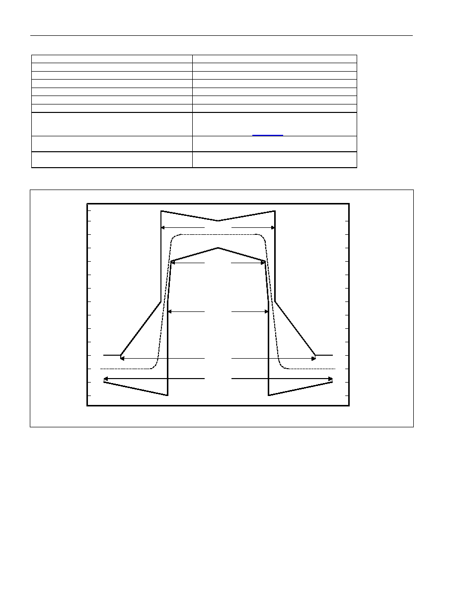
DS3251/DS3252/DS3253/DS3254
30 of 71
Table 9-E. E3 Waveform Test Parameters and Limits
PARAMETER SPECIFICATION
Rate
34.368Mbps (
±20ppm)
Line Code
HDB3
Transmission Medium
Coaxial cable (AT&T 734A or equivalent)
Test Measurement Point
At the transmitter
Test Termination
75
W (±1%) resistive
Pulse Amplitude
1.0V (nominal)
Pulse Shape
An isolated pulse (preceded by two zeros and
followed by one or more zeros) falls within the
template shown in
Figure 9-1
.
Ratio of the Amplitudes of Positive and Negative
Pulses at the Center of the Pulse Interval
0.95 to 1.05
Ratio of the Widths of Positive and Negative Pulses
at the Nominal Half Amplitude
0.95 to 1.05
Figure 9-1. E3 Waveform Template
0
-0.1
-0.2
0.1
0.2
0.3
0.4
0.5
0.6
0.7
0.8
0.9
1.0
1.1
1.2
TIME (ns)
G.703
E3
TEMPLATE
OUTP
UT LE
VE
L
(
V
)
29.1
24.5
12.1
8.65
17

DS3251/DS3252/DS3253/DS3254
31 of 71
Figure 9-2. DS3 AIS Structure
M1 Subframe
X1
(1)
84
Info
Bits
F1
(1)
84
Info
Bits
C1
(0)
84
Info
Bits
F2
(0)
84
Info
Bits
C2
(0)
84
Info
Bits
F3
(0)
84
Info
Bits
C3
(0)
84
Info
Bits
F4
(1)
84
Info
Bits
M2 Subframe
X2
(1)
84
Info
Bits
F1
(1)
84
Info
Bits
C1
(0)
84
Info
Bits
F2
(0)
84
Info
Bits
C2
(0)
84
Info
Bits
F3
(0)
84
Info
Bits
C3
(0)
84
Info
Bits
F4
(1)
84
Info
Bits
M3 Subframe
P1
(0)
84
Info
Bits
F1
(1)
84
Info
Bits
C1
(0)
84
Info
Bits
F2
(0)
84
Info
Bits
C2
(0)
84
Info
Bits
F3
(0)
84
Info
Bits
C3
(0)
84
Info
Bits
F4
(1)
84
Info
Bits
M4 Subframe
P2
(0)
84
Info
Bits
F1
(1)
84
Info
Bits
C1
(0)
84
Info
Bits
F2
(0)
84
Info
Bits
C2
(0)
84
Info
Bits
F3
(0)
84
Info
Bits
C3
(0)
84
Info
Bits
F4
(1)
84
Info
Bits
M5 Subframe
M1
(0)
84
Info
Bits
F1
(1)
84
Info
Bits
C1
(0)
84
Info
Bits
F2
(0)
84
Info
Bits
C2
(0)
84
Info
Bits
F3
(0)
84
Info
Bits
C3
(0)
84
Info
Bits
F4
(1)
84
Info
Bits
M6 Subframe
M2
(1)
84
Info
Bits
F1
(1)
84
Info
Bits
C1
(0)
84
Info
Bits
F2
(0)
84
Info
Bits
C2
(0)
84
Info
Bits
F3
(0)
84
Info
Bits
C3
(0)
84
Info
Bits
F4
(1)
84
Info
Bits
M7 Subframe
M3
(0)
84
Info
Bits
F1
(1)
84
Info
Bits
C1
(0)
84
Info
Bits
F2
(0)
84
Info
Bits
C2
(0)
84
Info
Bits
F3
(0)
84
Info
Bits
C3
(0)
84
Info
Bits
F4
(1)
84
Info
Bits
Note 1: X1 is transmitted first.
Note 2: The 84 info bits contain the repetitive sequence 1010..., where the first 1 in the sequence immediately follows each X, P, F, C, or M bit.

DS3251/DS3252/DS3253/DS3254
32 of 71
10. JITTER
ATTENUATOR
Each LIU contains an on-board jitter attenuator that can be placed in the receive path or the transmit path or can
be disabled. The TJA and RJA pins (hardware mode) or the
TCR
:TJA and
RCR
:RJA control bits (CPU bus mode)
specify how the jitter attenuator is used. Setting TJA = RJA = 0 disables the jitter attenuator. To use the jitter
attenuator in the receive path, set RJA = 1 (with TJA = 0). To use it in the transmit path, set TJA = 1.
Figure 10-1
shows the minimum jitter attenuation for the device when the jitter attenuator is enabled.
Figure 10-1
also shows
the receive jitter transfer when the jitter attenuator is disabled.
The jitter attenuator consists of a narrowband PLL to retime the selected clock, a FIFO to buffer the associated
data while the clock is being retimed, and logic to prevent FIFO over/underflow in the presence of very large jitter
amplitudes. In hardware mode, only 16-bit and 32-bit FIFO depths are available. See
Table 6-I
. In CPU bus mode,
control bits
TCR
:JAL[1:0] set the FIFO depth to 16, 32, 64, or 128 bits.
The jitter attenuator requires a transmission-quality master clock (i.e.,
±20ppm frequency accuracy and low jitter).
When enabled in the receive path, the JA can obtain its master clock from the appropriate MCLK pin, from the
clock adapter block, or from the TCLK pin. When enabled in the transmit path, the JA can take its master clock
from the MCLK pin or from the clock adapter block, but not from the TCLK pin. The CDR block also uses the
selected master clock. See Section
12
for more information about master clocks and clock selection.
The JA has a loop bandwidth of master_clock
∏ 2,058,874 (see corner frequencies in
Figure 10-1
). The JA
attenuates jitter at frequencies higher than the loop bandwidth, while allowing jitter (and wander) at lower
frequencies to pass through relatively unaffected.
In CPU bus mode the jitter attenuator indicates the fill status of its FIFO buffer in the JAFL (JA full) and JAEL (JA
empty) status bits in the
SRL
register. The JA sets the JAFL bit to indicate that its buffer is full. When the buffer
becomes full, the JA momentarily increases the frequency of the read clock by 6250 ppm to avoid buffer overflow
and consequent data loss. In a similar manner, the JA sets the JAEL bit to indicate that its buffer is empty. When
the buffer becomes empty, the JA momentarily decreases the frequency of the read clock by 6250 ppm to avoid
buffer underflow and consequent data errors. During these momentary frequency adjustments, jitter is passed
through the JA to avoid over/underflow. If the phase noise or frequency offset of the write clock is large enough to
cause the buffer to overflow or underflow, the JA sets both the JAFL bit and the JAEL bit to indicate that data errors
have occurred.
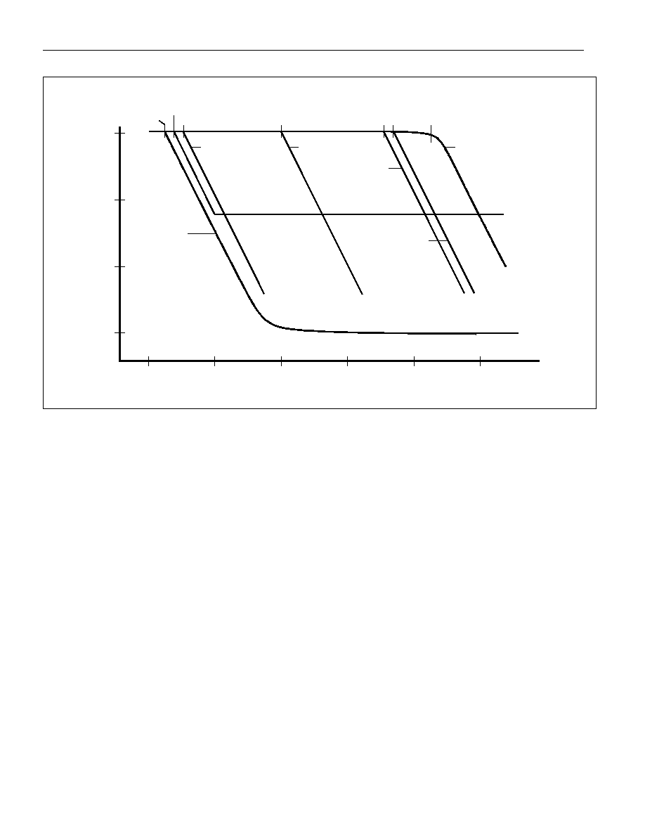
DS3251/DS3252/DS3253/DS3254
33 of 71
Figure 10-1. Jitter Attenuation/Jitter Transfer
10 100
1k
10k
100k
1M
21.7 Hz (DS3)
16.7 Hz (E3)
25.2 Hz (STS-1)
1k
-30
-20
-10
E3 [TBR24 (1997)]
FREQUENCY (Hz)
JIT
T
ER
AT
TEN
U
A
T
IO
N
(
d
B)
0
DS3 [GR-499 (1995)]
CATEGORY I
DS325x TYPICAL RECEIVER
JITTER TRANSFER WITH
JITTER ATTENUATOR
DISABLED
>150k
DS325x
DS3/E3/STS-1
MINIMUM
JITTER
ATTENUATION
WITH JITTER
ATTENUATOR
ENABLED
40Hz
DS3 [GR-253 (1999)]
CATEGORY I
27Hz
STS-1 [GR-253
(1999)] CATEGORY II
40k 59.6k
DS3 [GR-499 (1999)]
CATEGORY II
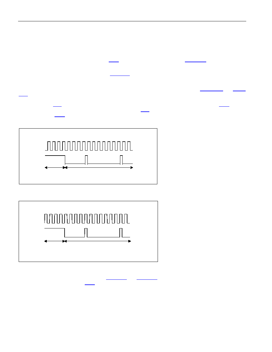
DS3251/DS3252/DS3253/DS3254
34 of 71
11. DIAGNOSTICS
11.1 PRBS Generator and Detector
Each LIU has built-in pseudorandom bit sequence (PRBS) generator and detector circuitry for physical layer
testing. The device generates and detects unframed 2
15
- 1 (DS3 or STS-1) or 2
23
- 1 PRBS, according to the ITU
O.151 specification. To transmit a PRBS pattern, pull the TDSA and TDSB pins high (hardware mode) or set
configuration bits TDSA and TDSB in the
GCR
register (CPU bus mode). As
Table 6-G
shows, the PRBS
generator automatically generates 2
15
- 1 for DS3 and STS-1 modes and 2
23
- 1 for E3 mode.
The PRBS detector, which is always enabled (
Table 6-H
), reports its status through the PRBS output pin (hardware
and CPU bus modes) or through the PRBS and PBER status bits (CPU bus mode). When the PRBS detector is out
of synchronization, the PRBS pin is forced high. When the detector syncs to an incoming PRBS pattern, the PRBS
pin is driven low, then pulses high, synchronous with RCLK, for each bit error detected. See
Figure 11-1
and
Figure
11-2
for details. In CPU bus mode, the PRBS status bit is set to one when the detector is out of synchronization
and set to zero when the detector syncs to an incoming PRBS pattern. A change of state of the PRBS bit sets the
PRBSL bit in the
SRL
register and can also cause an interrupt on the
INT pin if the PRBSIE bit in the
SRIE
register
is set to one. A pattern bit error set the PBERL bit in the
SRL
register and can also cause an interrupt if the
PBERIE bit in the
SRIE
register is set to one.
Figure 11-1. PRBS Output with Normal RCLK Operation
Figure 11-2. PRBS Output with Inverted RCLK Operation
11.2 Loopbacks
Each LIU has three internal loopbacks. See
Figure 4-1
and
Figure 4-2
. The LLB and RLB pins (hardware mode) or
LLB and RLB control bits in the
GCR
register (CPU bus mode) enable these loopbacks. When LLB = RLB = 0,
loopbacks are disabled. Setting RLB = 1 with LLB = 0 enables remote loopback, which loops recovered clock and
data back through the LIU transmitter. During remote loopback, recovered clock and data are output on RCLK,
RPOS/RDAT, and RNEG/RLCV, but the TPOS/TDAT and TNEG pins are ignored. Setting LLB = 1 with RLB = 0
enables analog local loopback, which loops the outgoing transmit signal back to the receiver's analog front end.
Setting LLB = RLB = 1 enables digital local loopback, which loops digital transmit clock and data back to the
receiver's digital circuitry, including the LOS detector, the B3ZS/HDB3 decoder, and the PRBS detector. When
either of the local loopbacks is enabled, the transmit signal is output normally on TXP/TXN, but the received signal
on RXP/RXN is ignored.
PRBS DETECTOR
IS NOT IN SYNC
PRBS DETECTOR IS IN SYNC; THE
PRBS PIN PULSES HIGH FOR EACH BIT
ERROR DETECTED
RCLK
PRBS
RCINV = 0
RCLK
PRBS
PRBS DETECTOR
IS NOT IN SYNC
PRBS DETECTOR IS IN SYNC; THE
PRBS PIN PULSES HIGH FOR EACH BIT
ERROR DETECTED
RCINV = 1

DS3251/DS3252/DS3253/DS3254
35 of 71
12. CLOCK ADAPTER
The clock adapter block generates all required clock rates from a single input clock. If a transmission-quality clock
of one line rate (DS3, E3 or STS-1) is present, the clock adapter can synthesize transmission-quality clocks at the
other two line rates. Both input clocks and synthesized clocks are then available to be used as master clocks by the
CDRs and jitter attenuators. In hardware mode the clock adapter is entirely controlled by the T3MCLK, E3MCLK
and STMCLK pins. See the pins descriptions for those pins in
Table 6-A
.
In CPU bus mode additional clock adapter control options are available in the
CACR
register. When control bit
AMCEN is set to 1, the clock adapter block is configured for alternate master clock mode. In this mode, the clock
adapter expects to receive a clock whose frequency is specified by the AMCSEL[1:0] control bits rather than a
DS3, E3 or STS-1 clock. Valid input frequencies are 19.44 MHz, 38.88 MHz and 77.76 MHz. In alternate master
clock mode the clock adapter can synthesize up to two clock rates (DS3, E3 or STS-1). To synthesize DS3 and E3
clocks, the alternate master clock should be applied to the STMCLK pin. To synthesize DS3 and STS-1 clocks, the
clock should be applied to the E3MCLK pin. To synthesize E3 and STS-1 clocks, the clock should be applied to the
T3MCLK pin. The device can be powered up with an alternate clock applied to one of the MCLK pins, even though
the power-on default values of AMCEN and AMCSEL[1:0] may not match the applied clock. Once these control bits
are properly set after power-up, the clock adapter begins to synthesize the proper master clocks, and the device as
a whole functions normally.
CPU bus mode also provides the ability to output synthesized master clocks on the T3MCLK, E3MCLK and
STMCLK pins for use by neighboring framers, mappers and other components. To output the synthesized DS3
master clock on T3MCLK, set
CACR
:T3MOE=1. To output the synthesized E3 master clock on E3MCLK, set
CACR
:E3MOE=1. To output the synthesized STS-1 master clock on STMCLK, set
CACR
:STMOE=1.
13. RESET LOGIC
There are four sources for reset: an internal power-on reset (POR) circuit, the reset pin
RST, the JTAG reset pin
JTRST, and the RST bit in each LIU's global configuration register (
GCR
). The chip is divided into three zones for
reset: the digital logic, the analog circuits, and the JTAG logic. The digital logic includes the status and control
registers, the B3ZS/HDB3 encoder and decoder, the PRBS generator and detector, and the LOS detect logic. The
analog circuits include clock and data recovery, jitter attenuator, and transmit waveform generation. The JTAG
logic consists of the common boundary scan controller and the boundary scan cells at each pin.
The POR circuit resets the digital logic, analog circuits, and JTAG logic zones. The
RST pin resets the digital logic
and the analog circuits but not the JTAG logic. The
JTRST pin resets only the JTAG logic. Each LIU's RST register
bit resets the digital logic for that LIU, including resetting the LIU's registers to the default state (except for the RST
bit itself).
The POR signal and
RST pin require an active master clock source for the LIU to properly reset.

DS3251/DS3252/DS3253/DS3254
36 of 71
14. TRANSFORMERS
Table 14-A. Transformer Characteristics
PARAMETER VALUE
Turns Ratio
1:2ct
±2%
Bandwidth 75
W
0.250MHz to 500MHz
(typ)
Primary Inductance
19
mH (min)
Leakage Inductance
0.150
mH (max)
Interwinding
Capacitance
10pF (max)
Isolation Voltage
1500V
RMS
(min)
Table 14-B. Recommended Transformers
MANUFACTURER
NO. OF
TRANSFORMERS
PART TEMP
RANGE
PIN-PACKAGE/
SCHEMATIC
1
PE-65968
0∞C to +70∞C
6 SMT
LS-1/C
1
PE-65969
0∞C to +70∞C
6 Thru-Hole
LC-1/C
Pulse Engineering
8
T3049
0∞C to +70∞C
32 SMT
YB/1
1
TG07-0206NS
0∞C to +70∞C
6 SMT
SMD/B
Halo Electronics
1
TD07-0206NE
0∞C to +70∞C
6 DIP
DIP/B
Note: Table subject to change. Industrial temperature range and multiport transformers are also available. Contact the manufacturers
for details at
www.pulseeng.com
and
www.haloelectronics.com
.

DS3251/DS3252/DS3253/DS3254
37 of 71
15. CPU INTERFACES
When the HW pin is logic 0 the device is in CPU bus mode. The default CPU interface is 8-bit parallel.
15.1 Parallel
Interface
When the device is in CPU bus mode, by default it presents a generic 8-bit parallel microprocessor interface. When
the MOT pin is logic 1, the interface is Motorola-style with
CS, R/W, and DS control lines. When MOT = 0, the
interface is Intel-style with
CS, RD, and WR control lines. In both styles, the interface supports both multiplexed and
nonmultiplexed operation. For multiplexed operation, wire A[5:0] to D[5:0], wire D[7:0] to the CPU's multiplexed
address/data bus, and connect the ALE pin to the appropriate pin on the micro. For nonmultiplexed operation, wire
ALE high and wire A[5:0] and D[7:0] to the appropriate pins on the micro. See
Table 17-H
,
Figure 17-3
and
Figure
17-4
for parallel interface timing diagrams and parameters.
15.2 SPI
Interface
When the MOT,
RD, and WR pins are all low, the device presents an SPI interface on the CS, SCLK, SDI, and
SDO pins. SPI is a widely-used master/slave bus protocol that allows a master device and one or more slave
devices to communicate over a serial bus. The DS325x is always a slave device. Masters are typically
microprocessors, ASICs or FPGAs. Data transfers are always initiated by the master device, which also generates
the SCLK signal. The DS325x receives serial data on the SDI pin and transmits serial data on the SDO pin. SDO is
high-impedance except when the DS325x is transmitting data to the bus master.
Clock Polarity and Phase. The CPOL pin defines the polarity of SCLK. When CPOL = 0, SCLK is normally low
and pulses high during bus transactions. When CPOL = 1, SCLK is normally high and pulses low during bus
transactions. the CPHA pin sets the phase (active edge) of SCLK. When CPHA = 0, data is latched in on SDI on
the leading edge of the SCLK pulse and updated on SDO on the trailing edge. When CPHA = 1, data is latched in
on SDI on the trailing edge of the SCLK pulse and updated on SDO on the following leading edge.
See
Figure 15-1
.
Bit Order. The control byte and all data bytes are transmitted MSB first on both SDI and SDO.
Device Selection. Each SPI device has its own chip-select line. To select the DS325x, pull its
CS pin low.
Control Byte. After
CS is pulled low, the bus master transmits the control byte during the first eight SCLK cycles.
The control byte has the form R/
W A5 A4 A3 A2 A1 A0 BURST, where A[5:0] is the register address, R/W is the
data direction bit (1 = read, 0 = write), and BURST is the burst bit (1 = burst access, 0 = single-byte access). In the
discussion that follows, a control byte with R/
W = 1 is a read control byte, while a control byte with R/W = 0 is a
write control byte.
Single-Byte Writes. See
Figure 15-2
. After
CS goes low, the bus master transmits a write control byte with
BURST = 0 followed by the data byte to be written. The bus master then terminates the transaction by pulling
CS
high.
Single-Byte Reads. See
Figure 15-2
. After
CS goes low, the bus master transmits a read control byte with
BURST = 0. The DS325x then responds with the requested data byte. The bus master then terminates the
transaction by pulling
CS high.
Burst Writes. See
Figure 15-2
. After
CS goes low, the bus master transmits a write control byte with BURST = 1
followed by the first data byte to be written. The DS325x receives the first data byte on SDI, writes it to the
specified register, increments its internal address register, and prepares to receive the next data byte. If the master
continues to transmit, the DS325x continues to write the data received and increment its address counter. After the
address counter reaches FFh it rolls over to address 00h and continues to increment.
Burst Reads. See
Figure 15-2
. After
CS goes low, the bus master transmits a read control byte with BURST = 1.
The DS325x then responds with the requested data byte on SDO, increments its address counter, and pre-fetches
the next data byte. If the bus master continues to demand data, the DS325x continues to provide the data on SDO,
increment its address counter, and pre-fetch the following byte. After the address counter reaches FFh it rolls over
to address 00h and continues to increment.

DS3251/DS3252/DS3253/DS3254
38 of 71
Early Termination of Bus Transactions. The bus master can terminate SPI bus transactions at any time by
pulling
CS high. In response to early terminations, the DS325x resets its SPI interface logic and waits for the start
of the next transaction. If a write transaction is terminated prior to the SCLK edge that latches the LSB of a data
byte, the current data byte is not written.
Design Option: Wiring SDI and SDO Together. Because communication between the bus master and the
DS325x is half-duplex, the SDI and SDO pins can be wired together externally to reduce wire count. To support
this option, the bus master must not drive the SDI/SDO line when the DS325x is transmitting.
AC Timing. See
Table 17-I
and
Figure 17-5
for AC timing specifications for the SPI interface.
Figure 15-1. SPI Clock Polarity and Phase Options
MSB
LSB
6
5
4
3
2
1
CS
SCK
SCK
SCK
SCK
SDI/SDO
CLOCK EDGE USED FOR DATA CAPTURE (ALL MODES)
CPOL = 0, CPHA = 0
CPOL = 0, CPHA = 1
CPOL = 1, CPHA = 0
CPOL = 1, CPHA = 1
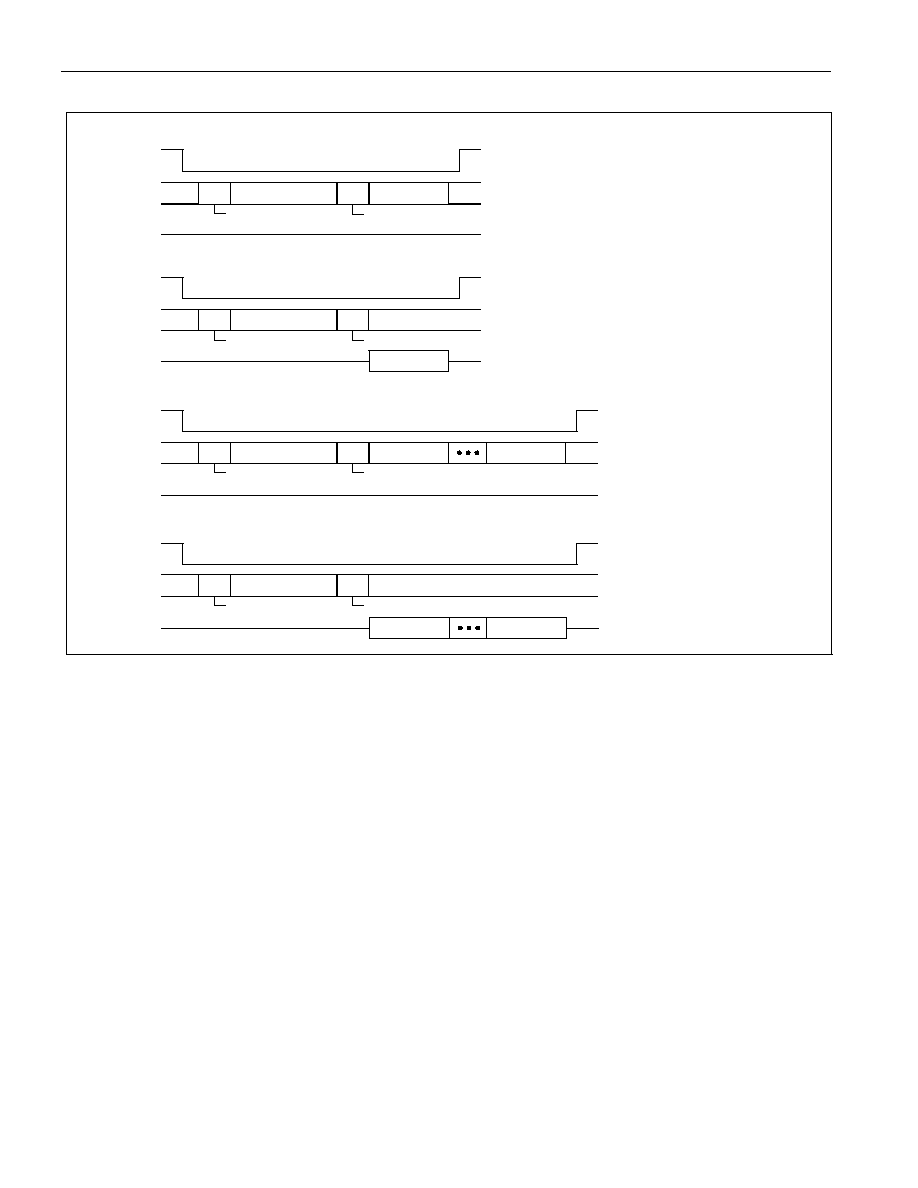
DS3251/DS3252/DS3253/DS3254
39 of 71
Figure 15-2. SPI Bus Transactions
R/
W Register Address Burst
Data Byte
SDI
CS
SDO
Single-Byte Write
Single-Byte Read
R/
W Register Address Burst
Data Byte
R/
W Register Address Burst Data Byte 1
Burst Write
SDI
CS
SDO
SDI
CS
SDO
0 (Write)
0 (single-byte)
1 (Read)
0 (single-byte)
0 (Write)
1 (burst)
Data Byte N
R/
W Register Address Burst
Data Byte 1
Burst Read
SDI
CS
1 (Read)
1 (burst)
Data Byte N
SDO

DS3251/DS3252/DS3253/DS3254
40 of 71
16. JTAG TEST ACCESS PORT AND BOUNDARY SCAN
16.1 JTAG
Description
The DS325x LIUs support the standard instruction codes SAMPLE/PRELOAD, BYPASS, and EXTEST. Optional
public instructions included are HIGHZ, CLAMP, and IDCODE.
Figure 16-1
features a block diagram. The LIUs
contain the following items, which meet the requirements set by the IEEE 1149.1 Standard Test Access Port and
Boundary Scan Architecture:
Test Access Port (TAP)
TAP
Controller
Instruction
Register
Bypass Register
Boundary Scan Register
Device Identification Register
The TAP has the necessary interface pins, namely JTCLK,
JTRST, JTDI, JTDO, and JTMS. Details on these pins
can be found in
Table 6-A
. Details about the boundary scan architecture and the TAP can be found in IEEE
1149.1-1990, IEEE 1149.1a-1993, and IEEE 1149.1b-1994.
16.2 JTAG TAP Controller State Machine Description
This section discusses the operation of the TAP controller state machine. The TAP controller is a finite state
machine that responds to the logic level at JTMS on the rising edge of JTCLK. Each of the states denoted in
Figure
16-2
are described in the following pages.
Test-Logic-Reset. Upon device power-up, the TAP controller starts in the Test-Logic-Reset state. The instruction
register contains the IDCODE instruction. All system logic on the device operates normally.
Run-Test-Idle. Run-Test-Idle is used between scan operations or during specific tests. The instruction and test
registers remain idle.
Select-DR-Scan. All test registers retain their previous state. With JTMS low, a rising edge of JTCLK moves the
controller into the Capture-DR state and initiates a scan sequence. JTMS high moves the controller to the Select-
IR-SCAN state.
Capture-DR. Data can be parallel loaded into the test data registers selected by the current instruction. If the
instruction does not call for a parallel load or the selected register does not allow parallel loads, the test register
remains at its current value. On the rising edge of JTCLK, the controller goes to the Shift-DR state if JTMS is low or
to the Exit1-DR state if JTMS is high.
Shift-DR. The test data register selected by the current instruction is connected between JTDI and JTDO and shifts
data one stage toward its serial output on each rising edge of JTCLK. If a test register selected by the current
instruction is not placed in the serial path, it maintains its previous state.
Exit1-DR. While in this state, a rising edge on JTCLK with JTMS high puts the controller in the Update-DR state,
which terminates the scanning process. A rising edge on JTCLK with JTMS low puts the controller in the Pause-DR
state.
Pause-DR. Shifting of the test registers is halted while in this state. All test registers selected by the current
instruction retain their previous state. The controller remains in this state while JTMS is low. A rising edge on
JTCLK with JTMS high puts the controller in the Exit2-DR state.
Exit2-DR. While in this state, a rising edge on JTCLK with JTMS high puts the controller in the Update-DR state
and terminates the scanning process. A rising edge on JTCLK with JTMS low puts the controller in the Shift-DR
state.
Update-DR. A falling edge on JTCLK while in the Update-DR state latches the data from the shift register path of
the test registers into the data output latches. This prevents changes at the parallel output because of changes in
the shift register. A rising edge on JTCLK with JTMS low puts the controller in the Run-Test-Idle state. With JTMS
high, the controller enters the Select-DR-Scan state.
Select-IR-Scan. All test registers retain their previous state. The instruction register remains unchanged during this
state. With JTMS low, a rising edge on JTCLK moves the controller into the Capture-IR state and initiates a scan
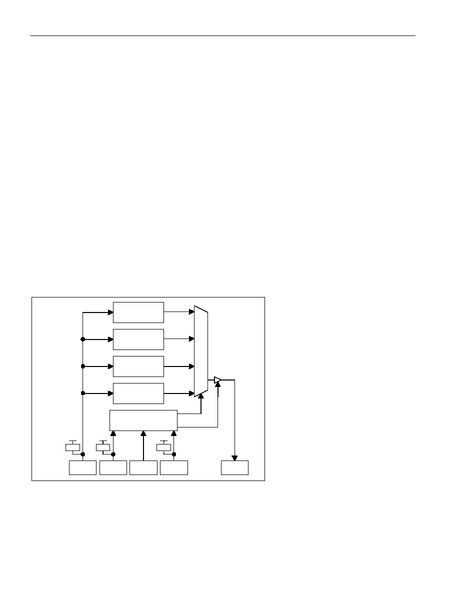
DS3251/DS3252/DS3253/DS3254
41 of 71
sequence for the instruction register. JTMS high during a rising edge on JTCLK puts the controller back into the
Test-Logic-Reset state.
Capture-IR. The Capture-IR state is used to load the shift register in the instruction register with a fixed value. This
value is loaded on the rising edge of JTCLK. If JTMS is high on the rising edge of JTCLK, the controller enters the
Exit1-IR state. If JTMS is low on the rising edge of JTCLK, the controller enters the Shift-IR state.
Shift-IR. In this state, the instruction register's shift register is connected between JTDI and JTDO and shifts data
one stage for every rising edge of JTCLK toward the serial output. The parallel register and the test registers
remain at their previous states. A rising edge on JTCLK with JTMS high moves the controller to the Exit1-IR state.
A rising edge on JTCLK with JTMS low keeps the controller in the Shift-IR state, while moving data one stage
through the instruction shift register.
Exit1-IR. A rising edge on JTCLK with JTMS low puts the controller in the Pause-IR state. If JTMS is high on the
rising edge of JTCLK, the controller enters the Update-IR state and terminates the scanning process.
Pause-IR. Shifting of the instruction register is halted temporarily. With JTMS high, a rising edge on JTCLK puts
the controller in the Exit2-IR state. The controller remains in the Pause-IR state if JTMS is low during a rising edge
on JTCLK.
Exit2-IR. A rising edge on JTCLK with JTMS high puts the controller in the Update-IR state. The controller loops
back to the Shift-IR state if JTMS is low during a rising edge of JTCLK in this state.
Update-IR. The instruction shifted into the instruction shift register is latched into the parallel output on the falling
edge of JTCLK as the controller enters this state. Once latched, this instruction becomes the current instruction. A
rising edge on JTCLK with JTMS low puts the controller in the Run-Test-Idle state. With JTMS high, the controller
enters the Select-DR-Scan state.
Figure 16-1. JTAG Block Diagram
BOUNDARY
SCAN
REGISTER
IDENTIFICATION
REGISTER
BYPASS
REGISTER
INSTRUCTION
REGISTER
TEST ACCESS PORT
CONTROLLER
MU
X
SELECT
TRI-STATE
JTDI
10k
JTMS
10k
JTCLK
JTRST
10k
JTDO
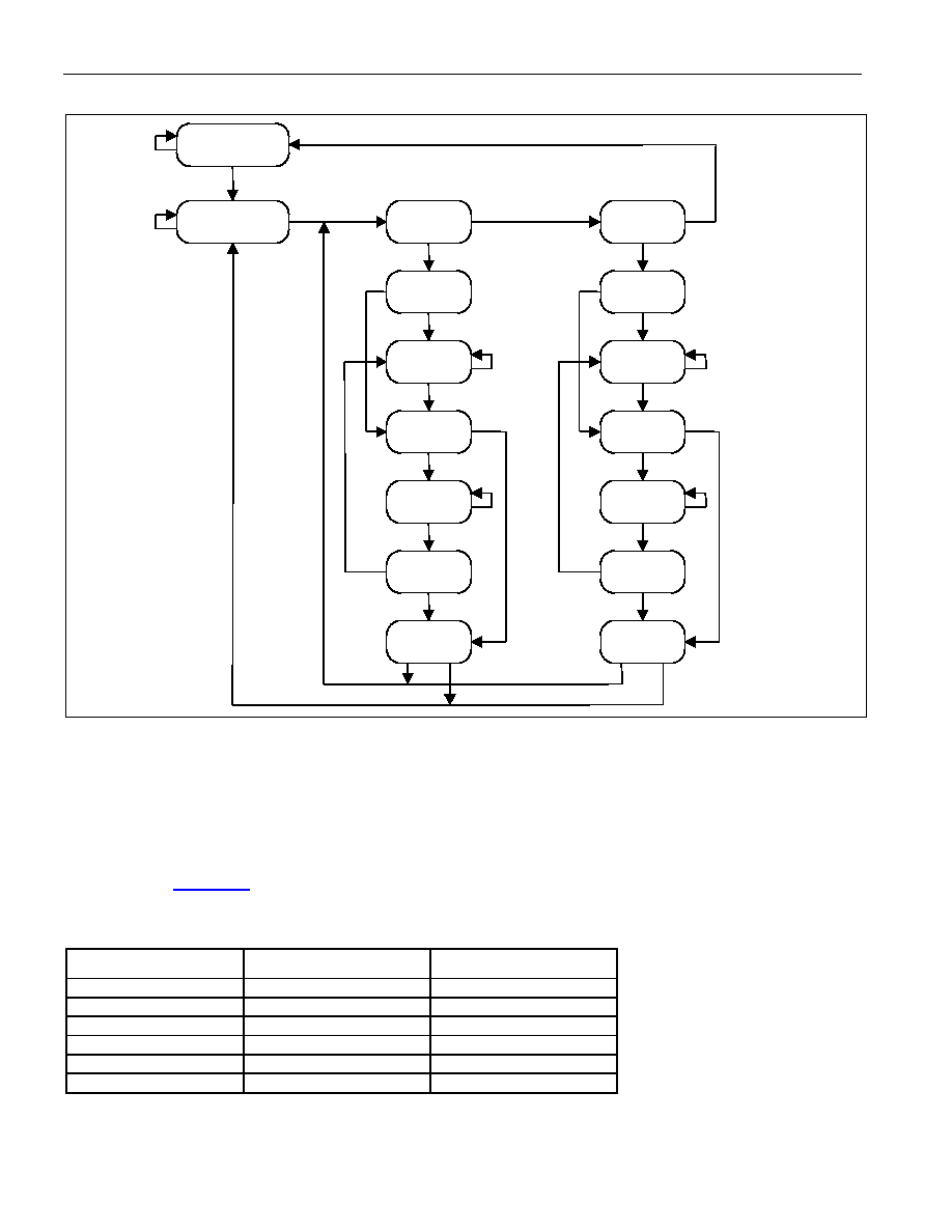
DS3251/DS3252/DS3253/DS3254
42 of 71
Figure 16-2. JTAG TAP Controller State Machine
16.3 JTAG Instruction Register and Instructions
The instruction register contains a shift register as well as a latched parallel output and is 3 bits in length. When the
TAP controller enters the Shift-IR state, the instruction shift register is connected between JTDI and JTDO. While in
the Shift-IR state, a rising edge on JTCLK with JTMS low shifts data one stage toward the serial output at JTDO. A
rising edge on JTCLK in the Exit1-IR state or the Exit2-IR state with JTMS high moves the controller to the Update-
IR state. The falling edge of that same JTCLK latches the data in the instruction shift register to the instruction
parallel output.
Table 16-A
shows the instructions supported by the DS325x and their respective operational binary
codes.
Table 16-A. JTAG Instruction Codes
INSTRUCTIONS SELECTED
REGISTER INSTRUCTION
CODES
SAMPLE/PRELOAD Boundary
Scan
010
BYPASS Bypass
111
EXTEST Boundary
Scan
000
CLAMP Bypass
011
HIGHZ Bypass 100
IDCODE Device
Identification
001
Test-Logic-Reset
Run-Test/Idle
Select
DR-Scan
1
0
Capture-DR
1
0
Shift-DR
0
1
Exit1- DR
1
0
Pause-DR
1
Exit2-DR
1
Update-DR
0
0
1
Select
IR-Scan
1
0
Capture-IR
0
Shift-IR
0
1
Exit1-IR
1
0
Pause-IR
1
Exit2-IR
1
Update-IR
0
0
1
0
0
1
0
1
0
1
DS3251/DS3252/DS3253/DS3254
43 of 71
SAMPLE/PRELOAD. SAMPLE/RELOAD is a mandatory instruction for the IEEE 1149.1 specification. This
instruction supports two functions. The digital I/Os of the device can be sampled at the boundary scan register
without interfering with the device's normal operation by using the Capture-DR state. SAMPLE/PRELOAD also
allows the DS325x to shift data into the boundary scan register through JTDI using the Shift-DR state.
EXTEST. EXTEST allows testing of the interconnections to the device. When the EXTEST instruction is latched in
the instruction register, the following actions occur. Once enabled through the Update-IR state, the parallel outputs
of the digital output pins are driven. The boundary scan register is connected between JTDI and JTDO. The
Capture-DR samples all digital inputs into the boundary scan register.
BYPASS. When the BYPASS instruction is latched into the parallel instruction register, JTDI connects to JTDO
through the 1-bit bypass test register. This allows data to pass from JTDI to JTDO without affecting the device's
normal operation.
IDCODE. When the IDCODE instruction is latched into the parallel instruction register, the identification test
register is selected. The device identification code is loaded into the identification register on the rising edge of
JTCLK, following entry into the Capture-DR state. Shift-DR can be used to shift the identification code out serially
through JTDO. During Test-Logic-Reset, the identification code is forced into the instruction register's parallel
output.
HIGHZ. All digital outputs are placed into a high-impedance state. The bypass register is connected between JTDI
and JTDO.
CLAMP. All digital output pins output data from the boundary scan parallel output while connecting the bypass
register between JTDI and JTDO. The outputs do not change during the CLAMP instruction.
Table 16-B. JTAG ID Code
PART REVISION DEVICE
CODE
MANUFACTURER
CODE
REQUIRED
DS3251 Consult
factory 0000000000101100
00010100001
1
DS3252 Consult
factory 0000000000101101
00010100001
1
DS3253 Consult
factory 0000000000101110
00010100001
1
DS3254 Consult
factory 0000000000101111
00010100001
1
16.4 JTAG Test Registers
IEEE 1149.1 requires a minimum of two test registers--the bypass register and the boundary scan register. An
optional test register, the identification register, has been included in the device design. It is used with the IDCODE
instruction and the Test-Logic-Reset state of the TAP controller.
Bypass Register. This is a single 1-bit shift register used with the BYPASS, CLAMP, and HIGHZ instructions,
which provide a short path between JTDI and JTDO.
Boundary Scan Register. This register contains a shift register path and a latched parallel output for control cells
and digital I/O cells. DS325x BSDL files are available at
www.maxim-ic.com/TechSupport/telecom/bsdl.htm
.
Identification Register. This register contains a 32-bit shift register and a 32-bit latched parallel output. It is
selected during the IDCODE instruction and when the TAP controller is in the Test-Logic-Reset state.

DS3251/DS3252/DS3253/DS3254
44 of 71
17. ELECTRICAL
CHARACTERISTICS
ABSOLUTE MAXIMUM RATINGS
Voltage Range on Any Lead with Respect to V
SS
(except V
DD
)....................................................-0.3V to +5.5V
Supply Voltage Range (V
DD
) with Respect to V
SS
....................................................................-0.3V to +3.63V
Ambient Operating Temperature Range................................................................................-40∞C to +85∞C
Junction Operating Temperature Range..............................................................................-40∞C to +125∞C
Storage Temperature Range.............................................................................................-55∞C to +125∞C
Soldering Temperature...................................................................See IPC/JEDEC J-STD-020 Specification
Stresses beyond those listed under "Absolute Maximum Ratings" may cause permanent damage to the device. These are stress ratings only,
and functional operation of the device at these or any other conditions beyond those indicated in the operational sections of the specifications is
not implied. Exposure to the absolute maximum rating conditions for extended periods may affect device. Ambient operating temperature range
when device is mounted on a four-layer JEDEC test board with no airflow.
Note: The typical values listed in Tables 17-A through 17-J are not production tested.
Table 17-A. Recommended DC Operating Conditions
(T
A
= -40∞C to +85∞C)
PARAMETER SYMBOL
CONDITIONS
MIN
TYP
MAX
UNITS
Supply Voltage
V
DD
3.135
3.3
3.465
V
Logic 1, All Other Input Pins
V
IH
2.0
5.5
V
Logic 0, All Other Input Pins
V
IL
-0.3
+0.8
V
Table 17-B. DC Characteristics
(V
DD
= 3.3V
±5%, T
A
= -40∞C to +85∞C.)
PARAMETER SYMBOL
CONDITIONS
MIN
TYP
MAX
UNITS
DS3251
80
120
DS3252
150
200
DS3253
220
280
Supply Current (Note 1)
I
DD
DS3254
290
360
mA
DS3251
60
100
DS3252
110
160
DS3253
160
220
Supply Current, Transmitters Tri-Stated
(All
TTSn Low) (Note 2)
I
DDTTS
DS3254
210
280
mA
Power-Down Current (All TPD, RPD
Control Bits High)
I
DDPD
DS325x
(Note 2)
35
50
mA
Lead Capacitance
C
IO
7 10 pF
Input Leakage, All Other Input Pins
I
IL
(Note
3)
-50 +10 mA
Output Leakage (when High-Z)
I
LO
(Note 3)
-10
+10
mA
Output Voltage (I
O
= -4.0mA)
V
OH
2.4
V
DD
V
Output Voltage (I
O
= +4.0mA)
V
OL
0
0.4 V
Note 1:
TCLKn = STMCLK = 51.84MHz; TXPn/TXNn driving all ones into 75
W resistive loads; analog loopback enabled; all other inputs
at V
DD
or grounded; all other outputs open.
Note 2:
TCLKn = STMCLK = 51.84MHz; other inputs at V
DD
or grounded; digital outputs left open circuited.
Note 3:
0V < V
IN
< V
DD
for all other digital inputs.
DS3251/DS3252/DS3253/DS3254
45 of 71
Table 17-C. Framer Interface Timing
(V
DD
= 3.3V
±5%, T
A
= -40∞C to +85∞C.) (
Figure 17-1
and
Figure 17-2
)
PARAMETER SYMBOL
CONDITIONS
MIN
TYP
MAX
UNITS
(Note 1)
22.4
(Note 2)
29.1
RCLK/TCLK Clock Period
t1
(Note 3)
19.3
ns
RCLK Duty Cycle
t2/t1, t3/t1
(Notes 4, 5)
45
50
55
%
TCLK Duty Cycle
t2/t1, t3/t1
(Note 5)
30
70
%
MCLK Duty Cycle
t2/t1, t3/t1
(Note 5)
30
70
%
TPOS/TDAT, TNEG to TCLK Setup
Time
t4 (Notes
5,
6) 2 ns
TPOS/TDAT, TNEG Hold Time
t5
(Notes 5, 6)
2
ns
RCLK to RPOS/RDAT, RNEG/RLCV,
and PRBS Value Change
t6
(Notes 4, 5, 7)
2
6
ns
RCLK Rise and Fall Time
t7
(Notes 5, 8)
3
5
ns
TCLK Rise and Fall Time
t8
(Notes 5, 9)
5
ns
Note 1:
DS3 mode.
Note 2:
E3 mode.
Note 3:
STS-1 mode.
Note 4:
Outputs loaded with 25pF, measured at 50% threshold.
Note 5:
Not tested during production test.
Note 6:
When TCINV = 0, TPOS/TDAT and TNEG are sampled on the rising edge of TCLK. When TCINV = 1, TPOS/TDAT and TNEG
are sampled on the falling edge of TCLK.
Note 7:
When RCINV = 0, RPOS/RDAT and RNEG/RLCV are updated on the falling edge of RCLK. When RCINV = 1, RPOS/RDAT and
RNEG/RLCV are updated on the rising edge of RCLK.
Note 8:
Outputs loaded with 25pF, measured between V
OL
(max) and V
OH
(min).
Note 9:
Measured between V
IL
(max) and V
IH
(min).

DS3251/DS3252/DS3253/DS3254
46 of 71
Figure 17-1. Transmitter Framer Interface Timing Diagram
Figure 17-2. Receiver Framer Interface Timing Diagram
TCLK (INVERTED)
TPOS/TDAT,
TNEG
t4
t5
t1
t2
t3
TCLK (NORMAL)
t8
RCLK (NORMAL)
RPOS/RDAT,
RNEG/RLCV
t6
t1
t2
t3
RCLK (INVERTED)
t7
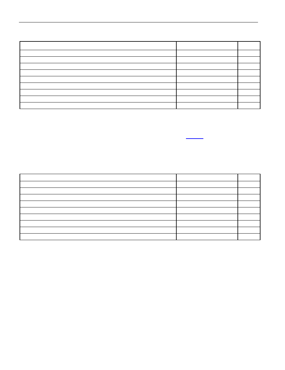
DS3251/DS3252/DS3253/DS3254
47 of 71
Table 17-D. Receiver Input Characteristics--DS3 and STS-1 Modes
(V
DD
= 3.3V
±5%, T
A
= -40∞C to +85∞C.)
PARAMETER MIN
TYP
MAX
UNITS
Receive Sensitivity (Length of Cable)
900
1200
ft
Signal-to-Noise Ratio, Interfering Signal Test (Notes 1, 2)
10
Input Pulse Amplitude, RMON = 0 (Notes 2, 3)
1000
mVpk
Input Pulse Amplitude, RMON = 1 (Note 2, 3)
200
mVpk
Analog LOS Declare, RMON = 0 (Note 4)
-24
dB
Analog LOS Clear, RMON = 0 (Note 4)
-21
dB
Analog LOS Declare, RMON = 1 (Note 4)
-38
dB
Analog LOS Clear, RMON = 1 (Note 4)
-35
dB
Intrinsic Jitter Generation (Note 2)
0.03
UI
P-P
Note 1:
An interfering signal (2
15
- 1 PRBS, B3ZS encoded, compliant waveshape, nominal bit rate) is added to the input signal. The
combined signal is passed through 0 to 900 feet of coaxial cable and presented to the DS325x receiver. This spec indicates the
lowest signal-to-noise ratio that results in a bit error ratio
£10
-9
.
Note 2:
Not tested during production test.
Note 3:
Measured on the line side (i.e., the BNC connector side) of the 1:2 receive transformer (
Figure 2-1
). During measurement,
incoming data traffic is unframed 2
15
- 1 PRBS.
Note 4:
With respect to nominal 800mVpk signal.
Table 17-E. Receiver Input Characteristics--E3 Mode
(V
DD
= 3.3V
±5%, T
A
= -40∞C to +85∞C.)
PARAMETER MIN
TYP
MAX
UNITS
Receive Sensitivity (Length of Cable)
900
1200
ft
Signal-to-Noise Ratio, Interfering Signal Test (Notes 1, 2)
12
Input Pulse Amplitude, RMON = 0 (Notes 2, 3)
1300
mVpk
Input Pulse Amplitude, RMON = 1 (Notes 2, 3)
260
mVpk
Analog LOS Declare, RMON = 0 (Note 4)
-24
dB
Analog LOS Clear, RMON = 0 (Note 4)
-21
dB
Analog LOS Declare, RMON = 1 (Note 4)
-38
dB
Analog LOS Clear, RMON = 1 (Note 4)
-35
dB
Intrinsic Jitter Generation (Note 2)
0.03
UI
P-P
Note 1:
An interfering signal (2
23
- 1 PRBS, HDB3 encoded, compliant waveshape, nominal bit rate) is added to the input signal. The
combined signal is passed through 0 to 900 feet of coaxial cable and presented to the DS325x receiver. This spec indicates the
lowest signal-to-noise ratio that results in a bit error ratio
£10
-9
.
Note 2:
Not tested during production test.
Note 3: Measured on the line side (i.e., the BNC connector side) of the 1:2 receive transformer (
Figure 2-1
). During measurement,
incoming data traffic is unframed 2
23
- 1 PRBS.
Note 4:
With respect to nominal 1000mVpk signal.

DS3251/DS3252/DS3253/DS3254
48 of 71
Table 17-F. Transmitter Output Characteristics--DS3 and STS-1 Modes
(V
DD
= 3.3V
±5%, T
A
= -40∞C to +85∞C.)
PARAMETER MIN
TYP
MAX
UNITS
DS3 Output Pulse Amplitude, TLBO = 0 (Note 1)
700
800
900
mVpk
DS3 Output Pulse Amplitude, TLBO = 1 (Note 1)
520
700
800
mVpk
STS-1 Output Pulse Amplitude, TLBO = 0 (Note 1)
700
800
1100
mVpk
STS-1 Output Pulse Amplitude, TLBO = 1 (Note 1)
520
700
850
mVpk
Ratio of Positive and Negative Pulse-Peak Amplitudes
0.9
1.1
DS3 Power Level at 22.368MHz (Note 2)
-1.8
+5.7
dBm
DS3 Power Level at 44.736MHz vs. Power Level at 22.368MHz (Note 2)
-20
dB
Intrinsic Jitter Generation (Note 3)
0.02
0.05
UI
P-P
Transmit Driver Monitor Minimum Threshold (V
TXMIN
), TLBO = 0
550
mVpk
Transmit Driver Monitor Minimum Threshold (V
TXMIN
), TLBO = 1
500
mVpk
Transmit Driver Monitor Maximum Threshold (V
TXMAX
), TLBO = 0
1050
mVpk
Transmit Driver Monitor Maximum Threshold (V
TXMAX
), TLBO = 1
800
mVpk
Note 1:
Measured on the line side (i.e., the BNC connector side) of the 2:1 transmit transformer (
Figure 2-1
).
Note 2:
Unframed all ones output signal, 3 kHz bandwidth, cable length 225 feet to 450 feet.
Note 3:
Measured with jitter-free clock applied to TCLK and a bandpass jitter filter with 10Hz and 800kHz cutoff frequencies. Not tested
during production test.
Table 17-G. Transmitter Output Characteristics--E3 Mode
(V
DD
= 3.3V
±5%, T
A
= -40∞C to +85∞C.)
PARAMETER MIN
TYP
MAX
UNITS
Output Pulse Amplitude (Note 1)
900
1000 1100
mVpk
Pulse
Width
14.55
ns
Ratio of Positive and Negative Pulse Amplitudes (at Centers of Pulses)
0.95
1.05
Ratio of Positive and Negative Pulse Widths (at Nominal Half Amplitude)
0.95
1.05
Intrinsic Jitter Generation (Note 2)
0.02
0.05
UI
P-P
Transmit Driver Monitor Minimum Threshold (V
TXMIN
)
750 mVpk
Transmit Driver Monitor Maximum Threshold (V
TXMAX
)
1250 mVpk
Note 1:
Measured on the line side (i.e., the BNC connector side) of the 2:1 transmit transformer (
Figure 2-1
).
Note 2:
Measured with jitter-free clock applied to TCLK and a bandpass jitter filter with 10Hz and 800kHz cutoff frequencies. Not tested
during production test.

DS3251/DS3252/DS3253/DS3254
49 of 71
Table 17-H. Parallel CPU Interface Timing
(V
DD
= 3.3V
±5%, T
A
= -40∞C to +85∞C.) (
Figure 17-3
and
Figure 17-4
)
PARAMETER SYMBOL
MIN
TYP
MAX
UNITS
Setup Time for A[5:0] Valid to
CS Active (Notes 1, 2)
t1 0 ns
Setup Time for
CS Active to RD, WR, or DS Active
t2 0 ns
Delay Time from
RD or DS Active to D[7:0] Valid
t3
65
ns
Hold Time from
RD or WR or DS Inactive to CS Inactive
t4 0 ns
Delay from
CS or RD or DS Inactive to D[7:0] Invalid or Tri-
State (Note 3)
t5 2
20 ns
Wait Time from
WR or DS Active to Latch D[7:0]
t6 65 ns
D[7:0] Setup Time to
WR or DS Inactive
t7 10 ns
D[7:0] Hold Time from
WR or DS Inactive
t8 2 ns
A[5:0] Hold Time from
WR or RD or DS Inactive
t9 5 ns
RD, WR, or DS Inactive Time
t10 75 ns
Muxed Address Valid to ALE Falling (Note 4)
t11
10
ns
Muxed Address Hold Time (Note 4)
t12
10
ns
ALE Pulse Width (Note 4)
t13
30
ns
Setup Time for ALE High or Muxed Address Valid to
CS
Active (Note 4)
t14 0 ns
Note 1:
D[7:0] loaded with 50pF when tested as outputs.
Note 2:
If a gapped clock is applied on TCLK and local loopback is enabled, read cycle time must be extended by the length of the largest
TCLK gap.
Note 3:
Not tested during production test.
Note 4:
In nonmultiplexed bus applications (
Figure 17-3
), ALE should be wired high. In multiplexed bus applications (
Figure 17-4
), A[5:0]
should be wired to D[5:0] and the falling edge of ALE latches the address.

DS3251/DS3252/DS3253/DS3254
50 of 71
Figure 17-3. Parallel CPU Interface Timing Diagram (Nonmultiplexed)
ADDRESS VALID
DATA VALID
A[5:0]
D[7:0]
WR
CS
RD
t1
t2 t3
t4
t5
t9
t10
INTEL READ CYCLE
ADDRESS VALID
A[5:0]
D[7:0]
RD
CS
WR
t1
t2 t6
t4
t7 t8
t9
t10
INTEL WRITE CYCLE

DS3251/DS3252/DS3253/DS3254
51 of 71
Figure 17-3. Parallel CPU Interface Timing Diagram (Nonmultiplexed)(continued)
ADDRESS VALID
DATA VALID
A[5:0]
D[7:0]
R/
W
CS
DS
t1
t2 t3
t4
t5
t9
t10
MOTOROLA READ CYCLE
ADDRESS VALID
A[5:0]
D[7:0]
R/
W
CS
DS
t1
t2 t6
t4
t7 t8
t9
t10
MOTOROLA WRITE CYCLE
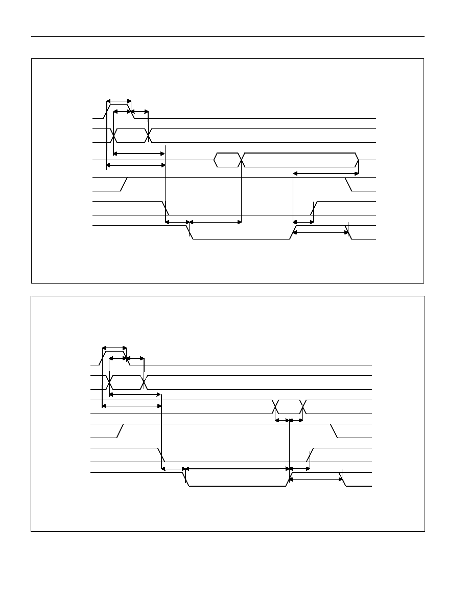
DS3251/DS3252/DS3253/DS3254
52 of 71
Figure 17-4. Parallel CPU Interface Timing Diagram (Multiplexed)
ADDRESS
VALID
DATA VALID
A[5:0]
D[7:0]
WR
CS
RD
t2 t3
t4
t5
t10
ALE
t11
t12
t13
t14
t14
NOTE: t14 STARTS ON THE OCCURRENCE OF EITHER THE RISING EDGE OF ALE OR A VALID ADDRESS, WHICHEVER OCCURS LAST.
NOTE: TO AVOID BUS CONTENTION, STOP DRIVING A[5:0] BEFORE
RD GOES LOW.
INTEL READ CYCLE
D[7:0]
RD
CS
WR
t2
t6 t4
t7
t8
t10
ADDRESS
VALID
A[5:0]
ALE
t11
t12
t13
t14
t14
NOTE: t14 STARTS ON THE OCCURRENCE OF EITHER THE RISING EDGE OF ALE OR A VALID ADDRESS, WHICHEVER OCCURS LAST.
INTEL WRITE CYCLE
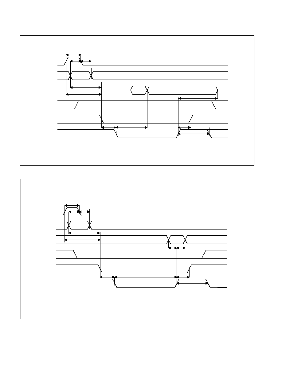
DS3251/DS3252/DS3253/DS3254
53 of 71
Figure 17-4. Parallel CPU Interface Timing Diagram (Multiplexed) (continued)
MOTOROLA READ CYCLE
DATA VALID
D[7:0]
R/
W
CS
DS
t2 t3
t4
t5
t10
ADDRESS
VALID
A[5:0]
ALE
t11
t12
t13
t14
t14
NOTE: t14 STARTS ON THE OCCURRENCE OF EITHER THE RISING EDGE OF ALE OR A VALID ADDRESS, WHICHEVER OCCURS LAST.
NOTE: TO AVOID BUS CONTENTION, STOP DRIVING A[5:0] BEFORE
RD GOES LOW.
D[7:0]
R/
W
A[5:0]
CS
DS
t2
t6
t4
t7 t8
t10
ADDRESS
VALID
ALE
t11
t12
t13
t14
t14
MOTOROLA WRITE CYCLE
NOTE: t14 STARTS ON THE OCCURRENCE OF EITHER THE RISING EDGE OF ALE OR A VALID ADDRESS, WHICHEVER OCCURS LAST.
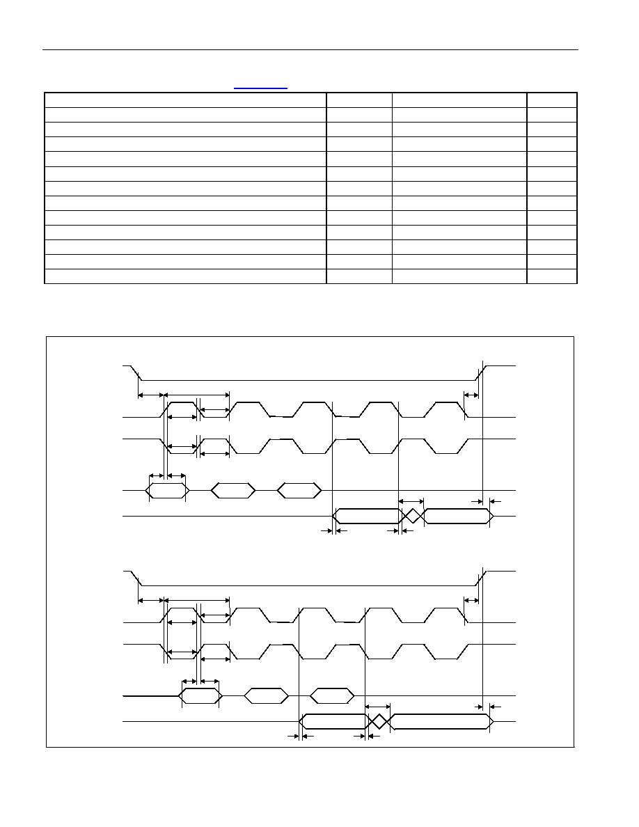
DS3251/DS3252/DS3253/DS3254
54 of 71
Table 17-I. SPI Interface Timing
(V
DD
= 3.3V
±5%, T
A
= -40∞C to +85∞C.) (
Figure 17-5
)
PARAMETER (Note 1)
SYMBOL
MIN
TYP
MAX
UNITS
SCLK Frequency
f
BUS
10
MHz
SCLK Cycle Time
t
CYC
100 ns
CS Setup to First SCLK Edge
t
SUC
15 ns
CS Hold time After Last SCLK Edge
t
HDC
15 ns
SCLK High Time
t
CLKH
50 ns
SCLK Low Time
t
CLKL
50 ns
SDI Data Setup Time
t
SUI
5 ns
SDI Data Hold Time
t
HDI
15 ns
SDO Enable Time (High-Impedance to Output Active)
t
EN
0 ns
SDO Disable Time (Output Active to High-Impedance)
t
DIS
25
ns
SDO Data Valid Time
t
DV
40
ns
SDO Data Hold Time After Update SCLK Edge
t
HDO
5 ns
Note 1:
All timing is specified with 100pF load on all SPI pins.
Figure 17-5. SPI Interface Timing Diagram
CS
SCLK,
CPOL=0
SCLK,
CPOL=1
t
SUI
t
HDI
SDI
t
CYC
t
SUC
t
CLKH
t
CLKL
t
CLKL
t
CLKH
t
HDC
SDO
t
EN
t
DV
t
HDO
t
DIS
CPHA = 0
CPHA = 1
CS
SCLK,
CPOL=0
SCLK,
CPOL=1
t
CYC
t
SUC
t
CLKH
t
CLKL
t
CLKL
t
HDC
t
SUI
t
HDI
SDI
SDO
t
EN
t
DV
t
HDO
t
DIS
t
CLKH
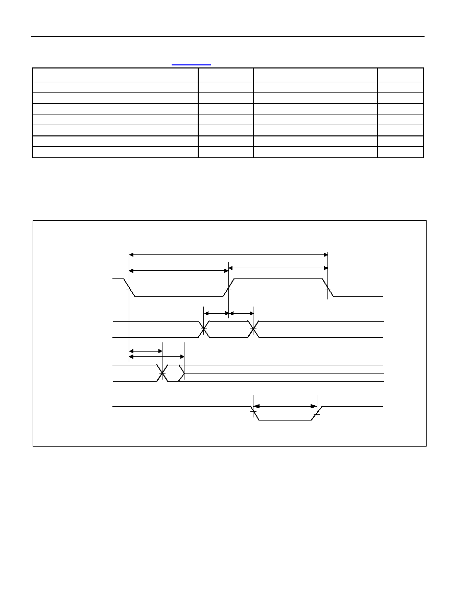
DS3251/DS3252/DS3253/DS3254
55 of 71
Table 17-J. JTAG Interface Timing
(V
DD
= 3.3V
±5%, T
A
= -40∞C to +85∞C.) (
Figure 17-6
)
PARAMETER SYMBOL
MIN
TYP
MAX
UNITS
JTCLK Clock Period
t1
1000
ns
JTCLK Clock High/Low Time (Note 1)
t2/t3
50
500
ns
JTCLK to JTDI, JTMS Setup Time
t4
50
ns
JTCLK to JTDI, JTMS Hold Time
t5
50
ns
JTCLK to JTDO Delay
t6
2
50
ns
JTCLK to JTDO High-Z Delay (Note 2)
t7
2
50
ns
JTRST Width Low Time
t8 100 ns
Note 1:
Clock can be stopped high or low.
Note 2:
Not tested during production test.
Figure 17-6. JTAG Timing Diagram
t1
JTDO
t4
t5
t2
t3
t7
JTDI, JTMS,
JTRST
t6
JTRST
t8
JTCLK

DS3251/DS3252/DS3253/DS3254
56 of 71
18. PIN
ASSIGNMENTS
Table 18-A
lists pin assignments sorted by signal name. DS3254 has all four LIUs. DS3253 has only LIUs 1, 2, and
3. DS3252 has only LIUs 1 and 2. DS3251 has only LIU 1.
Figure 18-1
through
Figure 18-11
show pinouts for the
four devices in both hardware and CPU bus modes.
Table 18-A. Pin Assignments Sorted by Signal Name
PIN
NAME
HARDWARE
MODE
PARALLEL
BUS MODE
SPI BUS
MODE
LIU 1
LIU 2
LIU 3
LIU 4
A0 N
Y
N
K6
A1 N
Y
N
L6
A2 N
Y
N
K7
A3 N
Y
N
L7
A4 N
Y
N
K8
A5 N
Y
N
L8
ALE N Y N
C7
CPHA N N Y
H3
CPOL N N Y
J3
CS
N Y Y
B7
D0 N
Y
N
E3
D1 N
Y
N
F2
D2 N
Y
N
F3
D3 N
Y
N
G2
D4 N
Y
N
G3
D5 N
Y
N
H2
D6 N
Y
N
H3
D7 N
Y
N
J3
E3MCLK Y Y Y
E12
E3Mn Y N N
F3
G10
C7
K6
HIZ
Y Y Y
J8
HW Y Y Y
E9
INT
N Y Y
C5
JTCLK Y Y Y
E4
JTDI Y Y Y
H4
JTDO Y Y Y
J4
JTMS Y Y Y
D5
JTRST
Y Y Y
D4
LLBn Y N N
B5
L8
E11
H2
MOT N Y Y
C6
PRBSn Y Y Y B1
L12
A11
M2
RBIN Y N N
D9
RCINV Y N N
J9
RCLKn Y Y Y C1
K12
A10
M3
RD / DS
N Y Y
B6
RJAn Y N N
B4
L9
D11
J2
RLBn Y N N
C5
K8
E10
H3
RLOSn
Y
Y
Y A1 M12 A12 M1

DS3251/DS3252/DS3253/DS3254
57 of 71
PIN
NAME
HARDWARE
MODE
PARALLEL
BUS MODE
SPI BUS
MODE
LIU 1
LIU 2
LIU 3
LIU 4
RNEGn / RLCVn
Y
Y
Y
C3
K10
C10
K3
RPOSn / RDATn
Y
Y
Y
C2
K11
B10
L3
RST
Y Y Y
H1
RTSn
Y
Y
Y B2 L11 B11 L2
RXNn Y Y Y A2
M11
B12
L1
RXPn Y Y Y
A3
M10
C12
K1
SCLK N N Y
F3
SDI N N Y
F2
SDO N N Y
E3
STMCLK Y Y Y
M8
STSn Y N N
F2
G11
B7
L6
T3MCLK Y Y Y
A5
TBIN Y N N
D8
TCINV Y N N
H9
TCLKn Y Y Y E1
H12
A8
M5
TDMn
Y Y Y
D3
J10
C9
K4
TDSAn Y N N G2
F11
B6
L7
TDSBn Y N N G3
F10
C6
K7
TEST
Y Y Y
J5
TJAn Y N N
C4
K9
D10
J3
TLBOn Y N N E3
H10
C8
K5
TNEGn Y Y Y D2
J11
B9
L4
TPOSn / TDATn
Y
Y
Y
D1
J12
A9
M4
TTSn
Y Y Y
E2
H11
B8
L5
TXNn Y Y Y
G1
F12
A6
M7
TXPn Y Y Y
F1
G12
A7
M6
V
DD
Y
Y
Y
D6, E5, E6, F4, F5, F6, G7, G8, G9, H7, H8, J7
V
SS
Y
Y
Y
D7, E7, E8, F7, F8, F9, G4, G5, G6, H5, H6, J6
WR / R/W
N Y Y
B5
DS3251/DS3252/DS3253/DS3254
58 of 71
Figure 18-1. DS3251 Hardware Mode Pin Assignment
A1
RLOS1
A2
RXN1
A3
RXP1
A4
RMON1
A5
T3MCLK
A6
N.C.
A7
N.C.
A8
N.C.
A9
N.C.
A10
N.C.
A11
N.C.
A12
N.C.
B1
PRBS1
B2
RTS1
B3
N.C.
B4
RJA1
B5
LLB1
B6
N.C.
B7
N.C.
B8
N.C.
B9
N.C.
B10
N.C.
B11
N.C.
B12
N.C.
C1
RCLK1
C2
RPOS1
C3
RNEG1
C4
TJA1
C5
RLB1
C6
N.C.
C7
N.C.
C8
N.C.
C9
N.C.
C10
N.C.
C11
N.C.
C12
N.C.
D1
TPOS1
D2
TNEG1
D3
TDM1
D4
JTRST
D5
JTMS
D6
V
DD
D7
V
SS
D8
TBIN
D9
RBIN
D10
N.C.
D11
N.C.
D12
N.C.
E1
TCLK1
E2
TTS1
E3
TLBO1
E4
JTCLK
E5
V
DD
E6
V
DD
E7
V
SS
E8
V
SS
E9
HW
E10
N.C.
E11
N.C.
E12
E3MCLK
F1
TXP1
F2
STS1
F3
E3M1
F4
V
DD
F5
V
DD
F6
V
DD
F7
V
SS
F8
V
SS
F9
V
SS
F10
N.C.
F11
N.C.
F12
N.C.
G1
TXN1
G2
TDSA1
G3
TDSB1
G4
V
SS
G5
V
SS
G6
V
SS
G7
V
DD
G8
V
DD
G9
V
DD
G10
N.C.
G11
N.C.
G12
N.C.
H1
RST
H2
N.C.
H3
N.C.
H4
JTDI
H5
V
SS
H6
V
SS
H7
V
DD
H8
V
DD
H9
TCINV
H10
N.C.
H11
N.C.
H12
N.C.
J1
N.C.
J2
N.C.
J3
N.C.
J4
JTDO
J5
TEST
J6
V
SS
J7
V
DD
J8
HIZ
J9
RCINV
J10
N.C.
J11
N.C.
J12
N.C.
K1
N.C.
K2
N.C.
K3
N.C.
K4
N.C.
K5
N.C.
K6
N.C.
K7
N.C.
K8
N.C.
K9
N.C.
K10
N.C.
K11
N.C.
K12
N.C.
L1
N.C.
L2
N.C.
L3
N.C.
L4
N.C.
L5
N.C.
L6
N.C.
L7
N.C.
L8
N.C.
L9
N.C.
L10
N.C.
L11
N.C.
L12
N.C.
M1
N.C.
M2
N.C.
M3
N.C.
M4
N.C.
M5
N.C.
M6
N.C.
M7
N.C.
M8
STMCLK
M9
N.C.
M10
N.C.
M11
N.C.
M12
N.C.
High-Speed Analog
High-Speed Digital
Low-Speed Digital
V
DD
V
SS
DS3251/DS3252/DS3253/DS3254
59 of 71
Figure 18-2. DS3251 Parallel Bus Mode Pin Assignment
A1
RLOS1
A2
RXN1
A3
RXP1
A4
N.C.
A5
T3MCLK
A6
N.C.
A7
N.C.
A8
N.C.
A9
N.C.
A10
N.C.
A11
N.C.
A12
N.C.
B1
PRBS1
B2
RTS1
B3
N.C.
B4
N.C.
B5
WR
B6
RD
B7
CS
B8
N.C.
B9
N.C.
B10
N.C.
B11
N.C.
B12
N.C.
C1
RCLK1
C2
RPOS1
C3
RNEG1
C4
N.C.
C5
INT
C6
MOT
C7
ALE
C8
N.C.
C9
N.C.
C10
N.C.
C11
N.C.
C12
N.C.
D1
TPOS1
D2
TNEG1
D3
TDM1
D4
JTRST
D5
JTMS
D6
V
DD
D7
V
SS
D8
N.C.
D9
N.C.
D10
N.C.
D11
N.C.
D12
N.C.
E1
TCLK1
E2
TTS1
E3
D0
E4
JTCLK
E5
V
DD
E6
V
DD
E7
V
SS
E8
V
SS
E9
HW
E10
N.C.
E11
N.C.
E12
E3MCLK
F1
TXP1
F2
D1
F3
D2
F4
V
DD
F5
V
DD
F6
V
DD
F7
V
SS
F8
V
SS
F9
V
SS
F10
N.C.
F11
N.C.
F12
N.C.
G1
TXN1
G2
D3
G3
D4
G4
V
SS
G5
V
SS
G6
V
SS
G7
V
DD
G8
V
DD
G9
V
DD
G10
N.C.
G11
N.C.
G12
N.C.
H1
RST
H2
D5
H3
D6
H4
JTDI
H5
V
SS
H6
V
SS
H7
V
DD
H8
V
DD
H9
N.C.
H10
N.C.
H11
N.C.
H12
N.C.
J1
N.C.
J2
N.C.
J3
D7
J4
JTDO
J5
TEST
J6
V
SS
J7
V
DD
J8
HIZ
J9
N.C.
J10
N.C.
J11
N.C.
J12
N.C.
K1
N.C.
K2
N.C.
K3
N.C.
K4
N.C.
K5
N.C.
K6
A0
K7
A2
K8
N.C.
K9
N.C.
K10
N.C.
K11
N.C.
K12
N.C.
L1
N.C.
L2
N.C.
L3
N.C.
L4
N.C.
L5
N.C.
L6
A1
L7
A3
L8
N.C.
L9
N.C.
L10
N.C.
L11
N.C.
L12
N.C.
M1
N.C.
M2
N.C.
M3
N.C.
M4
N.C.
M5
N.C.
M6
N.C.
M7
N.C.
M8
STMCLK
M9
N.C.
M10
N.C.
M11
N.C.
M12
N.C.
High-Speed Analog
High-Speed Digital
Low-Speed Digital
V
DD
V
SS

DS3251/DS3252/DS3253/DS3254
60 of 71
Figure 18-3. DS3251 SPI Bus Mode Pin Assignment
A1
RLOS1
A2
RXN1
A3
RXP1
A4
N.C.
A5
T3MCLK
A6
N.C.
A7
N.C.
A8
N.C.
A9
N.C.
A10
N.C.
A11
N.C.
A12
N.C.
B1
PRBS1
B2
RTS1
B3
N.C.
B4
N.C.
B5
WR
B6
RD
B7
CS
B8
N.C.
B9
N.C.
B10
N.C.
B11
N.C.
B12
N.C.
C1
RCLK1
C2
RPOS1
C3
RNEG1
C4
N.C.
C5
INT
C6
MOT
C7
N.C.
C8
N.C.
C9
N.C.
C10
N.C.
C11
N.C.
C12
N.C.
D1
TPOS1
D2
TNEG1
D3
TDM1
D4
JTRST
D5
JTMS
D6
V
DD
D7
V
SS
D8
N.C.
D9
N.C.
D10
N.C.
D11
N.C.
D12
N.C.
E1
TCLK1
E2
TTS1
E3
SDO
E4
JTCLK
E5
V
DD
E6
V
DD
E7
V
SS
E8
V
SS
E9
HW
E10
N.C.
E11
N.C.
E12
E3MCLK
F1
TXP1
F2
SDI
F3
SCLK
F4
V
DD
F5
V
DD
F6
V
DD
F7
V
SS
F8
V
SS
F9
V
SS
F10
N.C.
F11
N.C.
F12
N.C.
G1
TXN1
G2
N.C.
G3
N.C.
G4
V
SS
G5
V
SS
G6
V
SS
G7
V
DD
G8
V
DD
G9
V
DD
G10
N.C.
G11
N.C.
G12
N.C.
H1
RST
H2
N.C.
H3
CPHA
H4
JTDI
H5
V
SS
H6
V
SS
H7
V
DD
H8
V
DD
H9
N.C.
H10
N.C.
H11
N.C.
H12
N.C.
J1
N.C.
J2
N.C.
J3
CPOL
J4
JTDO
J5
TEST
J6
V
SS
J7
V
DD
J8
HIZ
J9
N.C.
J10
N.C.
J11
N.C.
J12
N.C.
K1
N.C.
K2
N.C.
K3
N.C.
K4
N.C.
K5
N.C.
K6
N.C.
K7
N.C.
K8
N.C.
K9
N.C.
K10
N.C.
K11
N.C.
K12
N.C.
L1
N.C.
L2
N.C.
L3
N.C.
L4
N.C.
L5
N.C.
L6
N.C.
L7
N.C.
L8
N.C.
L9
N.C.
L10
N.C.
L11
N.C.
L12
N.C.
M1
N.C.
M2
N.C.
M3
N.C.
M4
N.C.
M5
N.C.
M6
N.C.
M7
N.C.
M8
STMCLK
M9
N.C.
M10
N.C.
M11
N.C.
M12
N.C.
High-Speed Analog
High-Speed Digital
Low-Speed Digital
V
DD
V
SS
DS3251/DS3252/DS3253/DS3254
61 of 71
Figure 18-4. DS3252 Hardware Mode Pin Assignment
A1
RLOS1
A2
RXN1
A3
RXP1
A4
RMON1
A5
T3MCLK
A6
N.C.
A7
N.C.
A8
N.C.
A9
N.C.
A10
N.C.
A11
N.C.
A12
N.C.
B1
PRBS1
B2
RTS1
B3
N.C.
B4
RJA1
B5
LLB1
B6
N.C.
B7
N.C.
B8
N.C.
B9
N.C.
B10
N.C.
B11
N.C.
B12
N.C.
C1
RCLK1
C2
RPOS1
C3
RNEG1
C4
TJA1
C5
RLB1
C6
N.C.
C7
N.C.
C8
N.C.
C9
N.C.
C10
N.C.
C11
N.C.
C12
N.C.
D1
TPOS1
D2
TNEG1
D3
TDM1
D4
JTRST
D5
JTMS
D6
V
DD
D7
V
SS
D8
TBIN
D9
RBIN
D10
N.C.
D11
N.C.
D12
N.C.
E1
TCLK1
E2
TTS1
E3
TLBO1
E4
JTCLK
E5
V
DD
E6
V
DD
E7
V
SS
E8
V
SS
E9
HW
E10
N.C.
E11
N.C.
E12
E3MCLK
F1
TXP1
F2
STS1
F3
E3M1
F4
V
DD
F5
V
DD
F6
V
DD
F7
V
SS
F8
V
SS
F9
V
SS
F10
TDSB2
F11
TDSA2
F12
TXN2
G1
TXN1
G2
TDSA1
G3
TDSB1
G4
V
SS
G5
V
SS
G6
V
SS
G7
V
DD
G8
V
DD
G9
V
DD
G10
E3M2
G11
STS2
G12
TXP2
H1
RST
H2
N.C.
H3
N.C.
H4
JTDI
H5
V
SS
H6
V
SS
H7
V
DD
H8
V
DD
H9
TCINV
H10
TLBO2
H11
TTS2
H12
TCLK2
J1
N.C.
J2
N.C.
J3
N.C.
J4
JTDO
J5
TEST
J6
V
SS
J7
V
DD
J8
HIZ
J9
RCINV
J10
TDM2
J11
TNEG2
J12
TPOS2
K1
N.C.
K2
N.C.
K3
N.C.
K4
N.C.
K5
N.C.
K6
N.C.
K7
N.C.
K8
RLB2
K9
TJA2
K10
RNEG2
K11
RPOS2
K12
RCLK2
L1
N.C.
L2
N.C.
L3
N.C.
L4
N.C.
L5
N.C.
L6
N.C.
L7
N.C.
L8
LLB2
L9
RJA2
L10
N.C.
L11
RTS2
L12
PRBS2
M1
N.C.
M2
N.C.
M3
N.C.
M4
N.C.
M5
N.C.
M6
N.C.
M7
N.C.
M8
STMCLK
M9
RMON2
M10
RXP2
M11
RXN2
M12
RLOS2
High-Speed Analog
High-Speed Digital
Low-Speed Digital
V
DD
V
SS

DS3251/DS3252/DS3253/DS3254
62 of 71
Figure 18-5. DS3252 Parallel Bus Mode Pin Assignment
A1
RLOS1
A2
RXN1
A3
RXP1
A4
N.C.
A5
T3MCLK
A6
N.C.
A7
N.C.
A8
N.C.
A9
N.C.
A10
N.C.
A11
N.C.
A12
N.C.
B1
PRBS1
B2
RTS1
B3
N.C.
B4
N.C.
B5
WR
B6
RD
B7
CS
B8
N.C.
B9
N.C.
B10
N.C.
B11
N.C.
B12
N.C.
C1
RCLK1
C2
RPOS1
C3
RNEG1
C4
N.C.
C5
INT
C6
MOT
C7
ALE
C8
N.C.
C9
N.C.
C10
N.C.
C11
N.C.
C12
N.C.
D1
TPOS1
D2
TNEG1
D3
TDM1
D4
JTRST
D5
JTMS
D6
V
DD
D7
V
SS
D8
N.C.
D9
N.C.
D10
N.C.
D11
N.C.
D12
N.C.
E1
TCLK1
E2
TTS1
E3
D0
E4
JTCLK
E5
V
DD
E6
V
DD
E7
V
SS
E8
V
SS
E9
HW
E10
N.C.
E11
N.C.
E12
E3MCLK
F1
TXP1
F2
D1
F3
D2
F4
V
DD
F5
V
DD
F6
V
DD
F7
V
SS
F8
V
SS
F9
V
SS
F10
N.C.
F11
N.C.
F12
TXN2
G1
TXN1
G2
D3
G3
D4
G4
V
SS
G5
V
SS
G6
V
SS
G7
V
DD
G8
V
DD
G9
V
DD
G10
N.C.
G11
N.C.
G12
TXP2
H1
RST
H2
D5
H3
D6
H4
JTDI
H5
V
SS
H6
V
SS
H7
V
DD
H8
V
DD
H9
N.C.
H10
N.C.
H11
TTS2
H12
TCLK2
J1
N.C.
J2
N.C.
J3
D7
J4
JTDO
J5
TEST
J6
V
SS
J7
V
DD
J8
HIZ
J9
N.C.
J10
TDM2
J11
TNEG2
J12
TPOS2
K1
N.C.
K2
N.C.
K3
N.C.
K4
N.C.
K5
N.C.
K6
A0
K7
A2
K8
A4
K9
N.C.
K10
RNEG2
K11
RPOS2
K12
RCLK2
L1
N.C.
L2
N.C.
L3
N.C.
L4
N.C.
L5
N.C.
L6
A1
L7
A3
L8
N.C.
L9
N.C.
L10
N.C.
L11
RTS2
L12
PRBS2
M1
N.C.
M2
N.C.
M3
N.C.
M4
N.C.
M5
N.C.
M6
N.C.
M7
N.C.
M8
STMCLK
M9
N.C.
M10
RXP2
M11
RXN2
M12
RLOS2
High-Speed Analog
High-Speed Digital
Low-Speed Digital
V
DD
V
SS
DS3251/DS3252/DS3253/DS3254
63 of 71
Figure 18-6. DS3252 SPI Bus Mode Pin Assignment
A1
RLOS1
A2
RXN1
A3
RXP1
A4
N.C.
A5
T3MCLK
A6
N.C.
A7
N.C.
A8
N.C.
A9
N.C.
A10
N.C.
A11
N.C.
A12
N.C.
B1
PRBS1
B2
RTS1
B3
N.C.
B4
N.C.
B5
WR
B6
RD
B7
CS
B8
N.C.
B9
N.C.
B10
N.C.
B11
N.C.
B12
N.C.
C1
RCLK1
C2
RPOS1
C3
RNEG1
C4
N.C.
C5
INT
C6
MOT
C7
N.C.
C8
N.C.
C9
N.C.
C10
N.C.
C11
N.C.
C12
N.C.
D1
TPOS1
D2
TNEG1
D3
TDM1
D4
JTRST
D5
JTMS
D6
V
DD
D7
V
SS
D8
N.C.
D9
N.C.
D10
N.C.
D11
N.C.
D12
N.C.
E1
TCLK1
E2
TTS1
E3
SDO
E4
JTCLK
E5
V
DD
E6
V
DD
E7
V
SS
E8
V
SS
E9
HW
E10
N.C.
E11
N.C.
E12
E3MCLK
F1
TXP1
F2
SDI
F3
SCLK
F4
V
DD
F5
V
DD
F6
V
DD
F7
V
SS
F8
V
SS
F9
V
SS
F10
N.C.
F11
N.C.
F12
TXN2
G1
TXN1
G2
N.C.
G3
N.C.
G4
V
SS
G5
V
SS
G6
V
SS
G7
V
DD
G8
V
DD
G9
V
DD
G10
N.C.
G11
N.C.
G12
TXP2
H1
RST
H2
N.C.
H3
CPHA
H4
JTDI
H5
V
SS
H6
V
SS
H7
V
DD
H8
V
DD
H9
N.C.
H10
N.C.
H11
TTS2
H12
TCLK2
J1
N.C.
J2
N.C.
J3
CPOL
J4
JTDO
J5
TEST
J6
V
SS
J7
V
DD
J8
HIZ
J9
N.C.
J10
TDM2
J11
TNEG2
J12
TPOS2
K1
N.C.
K2
N.C.
K3
N.C.
K4
N.C.
K5
N.C.
K6
N.C.
K7
N.C.
K8
N.C.
K9
N.C.
K10
RNEG2
K11
RPOS2
K12
RCLK2
L1
N.C.
L2
N.C.
L3
N.C.
L4
N.C.
L5
N.C.
L6
N.C.
L7
N.C.
L8
N.C.
L9
N.C.
L10
N.C.
L11
RTS2
L12
PRBS2
M1
N.C.
M2
N.C.
M3
N.C.
M4
N.C.
M5
N.C.
M6
N.C.
M7
N.C.
M8
STMCLK
M9
N.C.
M10
RXP2
M11
RXN2
M12
RLOS2
High-Speed Analog
High-Speed Digital
Low-Speed Digital
V
DD
V
SS

DS3251/DS3252/DS3253/DS3254
64 of 71
Figure 18-7. DS3253 Hardware Mode Pin Assignment
A1
RLOS1
A2
RXN1
A3
RXP1
A4
RMON1
A5
T3MCLK
A6
TXN3
A7
TXP3
A8
TCLK3
A9
TPOS3
A10
RCLK3
A11
PRBS3
A12
RLOS3
B1
PRBS1
B2
RTS1
B3
N.C.
B4
RJA1
B5
LLB1
B6
TDSA3
B7
STS3
B8
TTS3
B9
TNEG3
B10
RPOS3
B11
RTS3
B12
RXN3
C1
RCLK1
C2
RPOS1
C3
RNEG1
C4
TJA1
C5
RLB1
C6
TDSB3
C7
E3M3
C8
TLBO3
C9
TDM3
C10
RNEG3
C11
N.C.
C12
RXP3
D1
TPOS1
D2
TNEG1
D3
TDM1
D4
JTRST
D5
JTMS
D6
V
DD
D7
V
SS
D8
TBIN
D9
RBIN
D10
TJA3
D11
RJA3
D12
RMON3
E1
TCLK1
E2
TTS1
E3
TLBO1
E4
JTCLK
E5
V
DD
E6
V
DD
E7
V
SS
E8
V
SS
E9
HW
E10
RLB3
E11
LLB3
E12
E3MCLK
F1
TXP1
F2
STS1
F3
E3M1
F4
V
DD
F5
V
DD
F6
V
DD
F7
V
SS
F8
V
SS
F9
V
SS
F10
TDSB2
F11
TDSA2
F12
TXN2
G1
TXN1
G2
TDSA1
G3
TDSB1
G4
V
SS
G5
V
SS
G6
V
SS
G7
V
DD
G8
V
DD
G9
V
DD
G10
E3M2
G11
STS2
G12
TXP2
H1
RST
H2
N.C.
H3
N.C.
H4
JTDI
H5
V
SS
H6
V
SS
H7
V
DD
H8
V
DD
H9
TCINV
H10
TLBO2
H11
TTS2
H12
TCLK2
J1
N.C.
J2
N.C.
J3
N.C.
J4
JTDO
J5
TEST
J6
V
SS
J7
V
DD
J8
HIZ
J9
RCINV
J10
TDM2
J11
TNEG2
J12
TPOS2
K1
N.C.
K2
N.C.
K3
N.C.
K4
N.C.
K5
N.C.
K6
N.C.
K7
N.C.
K8
RLB2
K9
TJA2
K10
RNEG2
K11
RPOS2
K12
RCLK2
L1
N.C.
L2
N.C.
L3
N.C.
L4
N.C.
L5
N.C.
L6
N.C.
L7
N.C.
L8
LLB2
L9
RJA2
L10
N.C.
L11
RTS2
L12
PRBS2
M1
N.C.
M2
N.C.
M3
N.C.
M4
N.C.
M5
N.C.
M6
N.C.
M7
N.C.
M8
STMCLK
M9
RMON2
M10
RXP2
M11
RXN2
M12
RLOS2
High-Speed Analog
High-Speed Digital
Low-Speed Digital
V
DD
V
SS

DS3251/DS3252/DS3253/DS3254
65 of 71
Figure 18-8. DS3253 Parallel Bus Mode Pin Assignment
A1
RLOS1
A2
RXN1
A3
RXP1
A4
N.C.
A5
T3MCLK
A6
TXN3
A7
TXP3
A8
TCLK3
A9
TPOS3
A10
RCLK3
A11
PRBS3
A12
RLOS3
B1
PRBS1
B2
RTS1
B3
N.C.
B4
N.C.
B5
WR
B6
RD
B7
CS
B8
TTS3
B9
TNEG3
B10
RPOS3
B11
RTS3
B12
RXN3
C1
RCLK1
C2
RPOS1
C3
RNEG1
C4
N.C.
C5
INT
C6
MOT
C7
ALE
C8
N.C.
C9
TDM3
C10
RNEG3
C11
N.C.
C12
RXP3
D1
TPOS1
D2
TNEG1
D3
TDM1
D4
JTRST
D5
JTMS
D6
V
DD
D7
V
SS
D8
N.C.
D9
N.C.
D10
N.C.
D11
N.C.
D12
N.C.
E1
TCLK1
E2
TTS1
E3
D0
E4
JTCLK
E5
V
DD
E6
V
DD
E7
V
SS
E8
V
SS
E9
HW
E10
N.C.
E11
N.C.
E12
E3MCLK
F1
TXP1
F2
D1
F3
D2
F4
V
DD
F5
V
DD
F6
V
DD
F7
V
SS
F8
V
SS
F9
V
SS
F10
N.C.
F11
N.C.
F12
TXN2
G1
TXN1
G2
D3
G3
D4
G4
V
SS
G5
V
SS
G6
V
SS
G7
V
DD
G8
V
DD
G9
V
DD
G10
N.C.
G11
N.C.
G12
TXP2
H1
RST
H2
D5
H3
D6
H4
JTDI
H5
V
SS
H6
V
SS
H7
V
DD
H8
V
DD
H9
N.C.
H10
N.C.
H11
TTS2
H12
TCLK2
J1
N.C.
J2
N.C.
J3
D7
J4
JTDO
J5
TEST
J6
V
SS
J7
V
DD
J8
HIZ
J9
N.C.
J10
TDM2
J11
TNEG2
J12
TPOS2
K1
N.C.
K2
N.C.
K3
N.C.
K4
N.C.
K5
N.C.
K6
A0
K7
A2
K8
A4
K9
N.C.
K10
RNEG2
K11
RPOS2
K12
RCLK2
L1
N.C.
L2
N.C.
L3
N.C.
L4
N.C.
L5
N.C.
L6
A1
L7
A3
L8
A5
L9
N.C.
L10
N.C.
L11
RTS2
L12
PRBS2
M1
N.C.
M2
N.C.
M3
N.C.
M4
N.C.
M5
N.C.
M6
N.C.
M7
N.C.
M8
STMCLK
M9
N.C.
M10
RXP2
M11
RXN2
M12
RLOS2
High-Speed Analog
High-Speed Digital
Low-Speed Digital
V
DD
V
SS
DS3251/DS3252/DS3253/DS3254
66 of 71
Figure 18-9. DS3253 SPI Bus Mode Pin Assignment
A1
RLOS1
A2
RXN1
A3
RXP1
A4
N.C.
A5
T3MCLK
A6
TXN3
A7
TXP3
A8
TCLK3
A9
TPOS3
A10
RCLK3
A11
PRBS3
A12
RLOS3
B1
PRBS1
B2
RTS1
B3
N.C.
B4
N.C.
B5
WR
B6
RD
B7
CS
B8
TTS3
B9
TNEG3
B10
RPOS3
B11
RTS3
B12
RXN3
C1
RCLK1
C2
RPOS1
C3
RNEG1
C4
N.C.
C5
INT
C6
MOT
C7
N.C.
C8
N.C.
C9
TDM3
C10
RNEG3
C11
N.C.
C12
RXP3
D1
TPOS1
D2
TNEG1
D3
TDM1
D4
JTRST
D5
JTMS
D6
V
DD
D7
V
SS
D8
N.C.
D9
N.C.
D10
N.C.
D11
N.C.
D12
N.C.
E1
TCLK1
E2
TTS1
E3
SDO
E4
JTCLK
E5
V
DD
E6
V
DD
E7
V
SS
E8
V
SS
E9
HW
E10
N.C.
E11
N.C.
E12
E3MCLK
F1
TXP1
F2
SDI
F3
SCLK
F4
V
DD
F5
V
DD
F6
V
DD
F7
V
SS
F8
V
SS
F9
V
SS
F10
N.C.
F11
N.C.
F12
TXN2
G1
TXN1
G2
N.C.
G3
N.C.
G4
V
SS
G5
V
SS
G6
V
SS
G7
V
DD
G8
V
DD
G9
V
DD
G10
N.C.
G11
N.C.
G12
TXP2
H1
RST
H2
N.C.
H3
CPHA
H4
JTDI
H5
V
SS
H6
V
SS
H7
V
DD
H8
V
DD
H9
N.C.
H10
N.C.
H11
TTS2
H12
TCLK2
J1
N.C.
J2
N.C.
J3
CPOL
J4
JTDO
J5
TEST
J6
V
SS
J7
V
DD
J8
HIZ
J9
N.C.
J10
TDM2
J11
TNEG2
J12
TPOS2
K1
N.C.
K2
N.C.
K3
N.C.
K4
N.C.
K5
N.C.
K6
N.C.
K7
N.C.
K8
N.C.
K9
N.C.
K10
RNEG2
K11
RPOS2
K12
RCLK2
L1
N.C.
L2
N.C.
L3
N.C.
L4
N.C.
L5
N.C.
L6
N.C.
L7
N.C.
L8
N.C.
L9
N.C.
L10
N.C.
L11
RTS2
L12
PRBS2
M1
N.C.
M2
N.C.
M3
N.C.
M4
N.C.
M5
N.C.
M6
N.C.
M7
N.C.
M8
STMCLK
M9
N.C.
M10
RXP2
M11
RXN2
M12
RLOS2
High-Speed Analog
High-Speed Digital
Low-Speed Digital
V
DD
V
SS
DS3251/DS3252/DS3253/DS3254
67 of 71
Figure 18-10. DS3254 Hardware Mode Pin Assignment
A1
RLOS1
A2
RXN1
A3
RXP1
A4
RMON1
A5
T3MCLK
A6
TXN3
A7
TXP3
A8
TCLK3
A9
TPOS3
A10
RCLK3
A11
PRBS3
A12
RLOS3
B1
PRBS1
B2
RTS1
B3
N.C.
B4
RJA1
B5
LLB1
B6
TDSA3
B7
STS3
B8
TTS3
B9
TNEG3
B10
RPOS3
B11
RTS3
B12
RXN3
C1
RCLK1
C2
RPOS1
C3
RNEG1
C4
TJA1
C5
RLB1
C6
TDSB3
C7
E3M3
C8
TLBO3
C9
TDM3
C10
RNEG3
C11
N.C.
C12
RXP3
D1
TPOS1
D2
TNEG1
D3
TDM1
D4
JTRST
D5
JTMS
D6
V
DD
D7
V
SS
D8
TBIN
D9
RBIN
D10
TJA3
D11
RJA3
D12
RMON3
E1
TCLK1
E2
TTS1
E3
TLBO1
E4
JTCLK
E5
V
DD
E6
V
DD
E7
V
SS
E8
V
SS
E9
HW
E10
RLB3
E11
LLB3
E12
E3MCLK
F1
TXP1
F2
STS1
F3
E3M1
F4
V
DD
F5
V
DD
F6
V
DD
F7
V
SS
F8
V
SS
F9
V
SS
F10
TDSB2
F11
TDSA2
F12
TXN2
G1
TXN1
G2
TDSA1
G3
TDSB1
G4
V
SS
G5
V
SS
G6
V
SS
G7
V
DD
G8
V
DD
G9
V
DD
G10
E3M2
G11
STS2
G12
TXP2
H1
RST
H2
LLB4
H3
RLB4
H4
JTDI
H5
V
SS
H6
V
SS
H7
V
DD
H8
V
DD
H9
TCINV
H10
TLBO2
H11
TTS2
H12
TCLK2
J1
RMON4
J2
RJA4
J3
TJA4
J4
JTDO
J5
TEST
J6
V
SS
J7
V
DD
J8
HIZ
J9
RCINV
J10
TDM2
J11
TNEG2
J12
TPOS2
K1
RXP4
K2
N.C.
K3
RNEG4
K4
TDM4
K5
TLBO4
K6
E3M4
K7
TDSB4
K8
RLB2
K9
TJA2
K10
RNEG2
K11
RPOS2
K12
RCLK2
L1
RXN4
L2
RTS4
L3
RPOS4
L4
TNEG4
L5
TTS4
L6
STS4
L7
TDSA4
L8
LLB2
L9
RJA2
L10
N.C.
L11
RTS2
L12
PRBS2
M1
RLOS4
M2
PRBS4
M3
RCLK4
M4
TPOS4
M5
TCLK4
M6
TXP4
M7
TXN4
M8
STMCLK
M9
RMON2
M10
RXP2
M11
RXN2
M12
RLOS2
High-Speed Analog
High-Speed Digital
Low-Speed Digital
V
DD
V
SS

DS3251/DS3252/DS3253/DS3254
68 of 71
Figure 18-11. DS3254 Parallel Bus Mode Pin Assignment
A1
RLOS1
A2
RXN1
A3
RXP1
A4
N.C.
A5
T3MCLK
A6
TXN3
A7
TXP3
A8
TCLK3
A9
TPOS3
A10
RCLK3
A11
PRBS3
A12
RLOS3
B1
PRBS1
B2
RTS1
B3
N.C.
B4
N.C.
B5
WR
B6
RD
B7
CS
B8
TTS3
B9
TNEG3
B10
RPOS3
B11
RTS3
B12
RXN3
C1
RCLK1
C2
RPOS1
C3
RNEG1
C4
N.C.
C5
INT
C6
MOT
C7
ALE
C8
N.C.
C9
TDM3
C10
RNEG3
C11
N.C.
C12
RXP3
D1
TPOS1
D2
TNEG1
D3
TDM1
D4
JTRST
D5
JTMS
D6
V
DD
D7
V
SS
D8
N.C.
D9
N.C.
D10
N.C.
D11
N.C.
D12
N.C.
E1
TCLK1
E2
TTS1
E3
D0
E4
JTCLK
E5
V
DD
E6
V
DD
E7
V
SS
E8
V
SS
E9
HW
E10
N.C.
E11
N.C.
E12
E3MCLK
F1
TXP1
F2
D1
F3
D2
F4
V
DD
F5
V
DD
F6
V
DD
F7
V
SS
F8
V
SS
F9
V
SS
F10
N.C.
F11
N.C.
F12
TXN2
G1
TXN1
G2
D3
G3
D4
G4
V
SS
G5
V
SS
G6
V
SS
G7
V
DD
G8
V
DD
G9
V
DD
G10
N.C.
G11
N.C.
G12
TXP2
H1
RST
H2
D5
H3
D6
H4
JTDI
H5
V
SS
H6
V
SS
H7
V
DD
H8
V
DD
H9
N.C.
H10
N.C.
H11
TTS2
H12
TCLK2
J1
N.C.
J2
N.C.
J3
D7
J4
JTDO
J5
TEST
J6
V
SS
J7
V
DD
J8
HIZ
J9
N.C.
J10
TDM2
J11
TNEG2
J12
TPOS2
K1
RXP4
K2
N.C.
K3
RNEG4
K4
TDM4
K5
N.C.
K6
A0
K7
A2
K8
A4
K9
N.C.
K10
RNEG2
K11
RPOS2
K12
RCLK2
L1
RXN4
L2
RTS4
L3
RPOS4
L4
TNEG4
L5
TTS4
L6
A1
L7
A3
L8
A5
L9
N.C.
L10
N.C.
L11
RTS2
L12
PRBS2
M1
RLOS4
M2
PRBS4
M3
RCLK4
M4
TPOS4
M5
TCLK4
M6
TXP4
M7
TXN4
M8
STMCLK
M9
N.C.
M10
RXP2
M11
RXN2
M12
RLOS2
High-Speed Analog
High-Speed Digital
Low-Speed Digital
V
DD
V
SS
DS3251/DS3252/DS3253/DS3254
69 of 71
Figure 18-12. DS3254 SPI Bus Mode Pin Assignment
A1
RLOS1
A2
RXN1
A3
RXP1
A4
N.C.
A5
T3MCLK
A6
TXN3
A7
TXP3
A8
TCLK3
A9
TPOS3
A10
RCLK3
A11
PRBS3
A12
RLOS3
B1
PRBS1
B2
RTS1
B3
N.C.
B4
N.C.
B5
WR
B6
RD
B7
CS
B8
TTS3
B9
TNEG3
B10
RPOS3
B11
RTS3
B12
RXN3
C1
RCLK1
C2
RPOS1
C3
RNEG1
C4
N.C.
C5
INT
C6
MOT
C7
N.C.
C8
N.C.
C9
TDM3
C10
RNEG3
C11
N.C.
C12
RXP3
D1
TPOS1
D2
TNEG1
D3
TDM1
D4
JTRST
D5
JTMS
D6
V
DD
D7
V
SS
D8
N.C.
D9
N.C.
D10
N.C.
D11
N.C.
D12
N.C.
E1
TCLK1
E2
TTS1
E3
SDO
E4
JTCLK
E5
V
DD
E6
V
DD
E7
V
SS
E8
V
SS
E9
HW
E10
N.C.
E11
N.C.
E12
E3MCLK
F1
TXP1
F2
SDI
F3
SCLK
F4
V
DD
F5
V
DD
F6
V
DD
F7
V
SS
F8
V
SS
F9
V
SS
F10
N.C.
F11
N.C.
F12
TXN2
G1
TXN1
G2
N.C.
G3
N.C.
G4
V
SS
G5
V
SS
G6
V
SS
G7
V
DD
G8
V
DD
G9
V
DD
G10
N.C.
G11
N.C.
G12
TXP2
H1
RST
H2
N.C.
H3
CPHA
H4
JTDI
H5
V
SS
H6
V
SS
H7
V
DD
H8
V
DD
H9
N.C.
H10
N.C.
H11
TTS2
H12
TCLK2
J1
N.C.
J2
N.C.
J3
CPOL
J4
JTDO
J5
TEST
J6
V
SS
J7
V
DD
J8
HIZ
J9
N.C.
J10
TDM2
J11
TNEG2
J12
TPOS2
K1
RXP4
K2
N.C.
K3
RNEG4
K4
TDM4
K5
N.C.
K6
N.C.
K7
N.C.
K8
N.C.
K9
N.C.
K10
RNEG2
K11
RPOS2
K12
RCLK2
L1
RXN4
L2
RTS4
L3
RPOS4
L4
TNEG4
L5
TTS4
L6
N.C.
L7
N.C.
L8
N.C.
L9
N.C.
L10
N.C.
L11
RTS2
L12
PRBS2
M1
RLOS4
M2
PRBS4
M3
RCLK4
M4
TPOS4
M5
TCLK4
M6
TXP4
M7
TXN4
M8
STMCLK
M9
N.C.
M10
RXP2
M11
RXN2
M12
RLOS2
High-Speed Analog
High-Speed Digital
Low-Speed Digital
V
DD
V
SS
DS3251/DS3252/DS3253/DS3254
70 of 71
19. PACKAGE
INFORMATION
(The package drawing(s) in this data sheet may not reflect the most current specifications. For the latest package outline
information, go to
www.maxim-ic.com/DallasPackInfo
.)
BOTTOM VIEW
12 11 10 9 8 7 6 5
4
3
2
1
1.00
A1 BALL PAD CORNER
A
B
C
D
E
F
G
H
J
K
L
M
(1.00)
(1.00)
1.00
13.00
13.00
Note: All dimensions in millimeters.
DS3251/DS3252/DS3253/DS3254
71 of 71
Maxim/Dallas Semiconductor cannot assume responsibility for use of any circuitry other than circuitry entirely embodied in a Maxim/Dallas Semiconductor product.
No circuit patent licenses are implied. Maxim/Dallas Semiconductor reserves the right to change the circuitry and specifications without notice at any time.
Ma xi m I nt e gr at e d Pr o du ct s, 1 2 0 S a n G abr i el Dr i ve, S un n yv al e, C A 94 0 8 6 40 8- 7 37- 7 60 0
© 2005 Maxim Integrated Products
∑ Printed USA
The Maxim logo is a registered trademark of Maxim Integrated Products, Inc. The Dallas logo is a registered trademark of Dallas Semiconductor Corporation.
20. THERMAL
INFORMATION
Table 20-A. Thermal Properties, Natural Convection
PARAMETER MIN
TYP
MAX
Ambient Temperature (Note 1)
-40
∞C
--
+85
∞C
Junction Temperature
-40
∞C
--
+125
∞C
Theta-JA (
q
JA
), Still Air (Note 2)
22.4
∞C/W
Psi-JB
9.2
∞C/W
Psi-JT
1.6
∞C/W
Note 1: The package is mounted on a four-layer JEDEC standard test board with no airflow and dissipating maximum power.
Note 2: Theta-JA (
q
JA
) is the junction to ambient thermal resistance, when the package is mounted on a four-layer JEDEC standard test board
with no airflow and dissipating maximum power.
Table 20-B. Theta-JA (
q
JA
) vs. Airflow
FORCED AIR (METERS PER
SECOND)
THETA-JA (
q
JA
)
0
22.4
∞C/W
1
19.0
∞C/W
2.5
17.2
∞C/W
21. REVISION
HISTORY
REVISION DESCRIPTION
031805
New Product Release (DS3254)
061705
New Product Release (DS3251/DS3252/DS3253)