1 of 10
REV: 041603
Note: Some revisions of this device may incorporate deviations from published specifications known as errata. Multiple revisions of any device
may be simultaneously available through various sales channels. For information about device errata, click here:
www.maxim-ic.com/errata
.
GENERAL DESCRIPTION
The DS32kHz is a temperature-compensated crystal
oscillator (TCXO) with an output frequency of
32.768kHz. This device addresses applications
requiring better timekeeping accuracy and can be
used to drive the X1 input of most Dallas
Semiconductor real-time clocks (RTCs), chipsets, and
other ICs containing RTCs. This device is available in
commercial (DS32kHz) and industrial (DS32kHz-N)
temperature versions.
APPLICATIONS
GPS Receivers
Telematics
Network Timing and Synchronization in Servers,
Routers, Hubs, and Switches
Automatic Power Meters
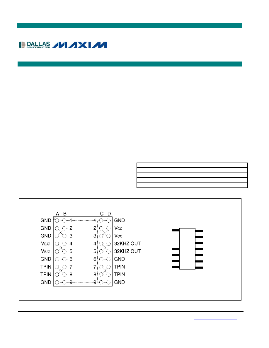
PIN CONFIGURATIONS
FEATURES
�
Accurate to �4 Min/Yr (-40�C to +85�C)
�
Accurate to �1 Min/Yr (0�C to +40�C)
�
Battery Backup for Continuous Timekeeping
�
V
BAT
Operating Voltage: 2.7V to 5.5V with V
CC
Grounded
�
V
CC
Operating Voltage: 4.5V to 5.5V
�
Operating Temperature Range:
0�C to +70�C (Commercial)
-40�C to +85�C (Industrial)
�
No Calibration Required
�
Low-Power Consumption
�
Surface Mountable Using BGA Package
�
UL Recognized
ORDERING INFORMATION
PART TEMP
RANGE
PIN-PACKAGE
DS32kHz/DIP
0�C to +70�C
14 DIP
DS32kHz-N/DIP
-40�C to +85�C
14 DIP
DS32kHz/WBGA
0�C to +70�C
36 BGA
DS32kHz-N/WBGA
-40�C to +85�C
36 BGA
DS32kHz
32.768kHz Temperature-Compensated
Crystal Oscillator
www.maxim-ic.com
BGA
TOP VIEW
N.C.
V
CC
32KHZ OUT
TPIN
TPIN
N.C.
N.C.
1
2
3
4
5
6
7
14
13
12
11
10
9
8
DIP
N.C.
GND
V
BAT
N.C.
N.C.
DS3
2
k
Hz

DS32kHz
2 of 10
ABSOLUTE MAXIMUM RATINGS
Voltage Range on Any Pin Relative to Ground
-3.0V to +7.0V
Operating Temperature Range
Commercial
0�C to +70�C
Industrial
-40�C to +85�C
Storage Temperature Range
-40�C to +85�C
Soldering Temperature (BGA)
See IPC/JEDEC J-STD-020A (2x max) (Note 1)
Soldering Temperature, Leads (DIP)
260�C for 10 seconds (Notes 1, 2)
Stresses beyond those listed under "Absolute Maximum Ratings" may cause permanent damage to the device. These are stress ratings only,
and functional operation of the device at these or any other conditions beyond those indicated in the operational sections of the specifications is
not implied. Exposure to the absolute maximum rating conditions for extended periods may affect device.
RECOMMENDED DC OPERATING CONDITIONS
(T
A
= -40�C to +85�C)
PARAMETER SYMBOL
CONDITIONS
MIN
TYP
MAX
UNITS
Power-Supply Voltage
V
CC
4.5 5.0 5.5 V
Battery Voltage (Note 3)
V
BAT
2.7 3.0
3.3,
5.5 V
DC ELECTRICAL CHARACTERISTICS
(Over the operating range, unless otherwise specified.)
PARAMETER SYMBOL
CONDITIONS
MIN
TYP
MAX
UNITS
Active Supply Current
I
CC
(Notes
4,
5)
150 180 �A
Active Battery Current
I
BAT
V
CC
= 0V, V
BAT
= 3.3V
(Notes 4, 5, 6, 7)
1 4 �A
High Output Voltage (V
CC
) V
OH
I
OH
= -1.0mA
2.4
V
Low Output Voltage
V
OL
I
OL
= 2.1mA
0.4
V
Battery Switch Voltage
V
SW
V
BAT
V
High Output Voltage (V
BAT
) V
OH
I
OH
= -0.1mA
2.4
V
Note 1: Post-solder cleaning with water-washing techniques is acceptable, provided that ultrasonic vibration is not used. Such cleaning can
damage the crystal.
Note 2: Encapsulated DIP modules can be successfully processed through conventional wave-soldering techniques, as long as the temperature
of the crystal contained inside does not exceed +150�C.
Note 3: V
BAT
must be no greater than 3.3V when the device is used in the dual-supply operating modes.
Note 4: Typical values are at +25�C and 5.0V V
CC
, 3.0 V
BAT
, unless otherwise indicated.
Note 5: These parameters are measured under no load conditions.
Note 6: This current is the active mode current sourced from the backup supply/battery.
Note 7:
Battery current increases to 450�A (typ) for 122ms (typ) for every 64 seconds.

DS32kHz
3 of 10
AC TIMING CHARACTERISTICS
(Over the operating range, unless otherwise specified.)
PARAMETER SYMBOL
CONDITIONS
MIN
TYP
MAX
UNITS
Output Frequency
f
OUT
32.768 kHz
0�C to +40�C
-2.0
+2.0
Frequency Stability vs.
Temperature
f/f
O
-40�C to +85�C or
0�C to +70�C
-7.5 +7.5
ppm
Duty Cycle
t
W
/t
45 50 55 %
Cycle Time
t
CYC
(Note
8)
30.518
�s
High/Low Time
t
H
/t
L
(Note
8)
15.06 �s
Rise Time
t
R
(Note
8)
200 ns
Fall Time
t
F
(Note
8)
60 ns
Oscillator Startup Time
t
OSC
(Note
8)
1 s
Frequency Stability vs.
Operating Voltage
f/
V
V
CC
= 5.0V or
V
BAT
= 3.0V, V
CC
= 0V
(Notes 4, 9)
�2.5 ppm/
V
Crystal Aging
f/f
O
(Notes
4,
10)
�1.0 ppm/yr
Note 8: These parameters are measured using a 15pF load.
Note 9: Error is measured from the nominal supply voltage of whichever supply is powering the device.
Note 10: After reflow.

DS32kHz
4 of 11
TYPICAL OPERATING CHARACTERISTICS
(V
CC
= 3.3V, T
A
= +25�C, unless otherwise noted.)
FREQUENCY ERROR vs. V
CC
DS32kHZ toc05
V
CC
(V)
ERROR (ppm)
5.0
-0.5
0
0.5
1.0
1.5
2.0
-1.0
4.5
5.5
FREQUENCY ERROR vs. V
BAT
DS32kHZ toc04
VBAT (V)
ERROR (ppm)
5.0
4.5
4.0
3.5
3.0
0
1
2
3
4
5
6
7
8
-1
2.5
5.5
I
BAT
vs. OUTPUT LOAD vs. V
CC
DS32kHZ toc03
V
BAT
SUPPLY CURRENT (
m
A)
5.0
4.5
4.0
3.5
3.0
2.50
6.00
7.50
10.0
12.5
15.0
0
2.5
5.5
47pF
22pF
10pF
0pF
I
CC
vs. V
CC
DS32kHZ toc02
V
CC
(V)
SUPPLY CURRENT (
m
A)
5.0
4.5
4.0
3.5
3.0
50
75
100
125
150
25
2.5
5.5
I
BAT
vs. V
BAT
DS32kHZ toc01
V
BAT
(V)
SUPPLY CURRENT (
m
A)
5.0
4.5
4.0
3.5
3.0
2.0
2.5
3.0
3.5
4.0
4.5
1.5
2.5
5.5
DS32kHz
5 of 10
PIN DESCRIPTIONS
PIN
BGA DIP
NAME FUNCTION
A4, A5, B4, B5
5
V
BAT
+3V Batttery Supply
A7, A8, B7, B8,
C7, C8, D7, D8
10, 11
TPIN
Test Pin (must be grounded)
C2, C3, D2, D3
13
V
CC
Primary Power Supply
C4, C5, D4, D5
12
32KHZ OUT
32.768kHz Output
--
1, 6�9, 14
N.C.
No Connection
All remaining balls
4
GND
Ground
Figure 1. Delta Time and Frequency vs. Temperature
FUNCTIONAL DESCRIPTION
The DS32kHz requires four pins for operation: V
CC
, GND, V
BAT
, and 32KHZ OUT. (See Figure 3 for connection
schemes.) Power is applied through V
CC
and GND, while V
BAT
is used to maintain the 32kHz output in the absence
of power. The output is accurate to �7.5ppm (�4 min/yr) from �40�C to +85�C and �2ppm (�1 min/yr) from 0�C to
+40�C.
The DS32kHz is packaged in a small 36-pin SMD using ball grid array (BGA) technology
with dimensions 0.400" wide, 0.450" long, and 0.124" high. It also is available in a 14-pin DIP module.
The additional board space required is negligible in most applications and, therefore, the recommended land
pattern layout should be implemented on all new designs and future board revisions to satisfy applications requiring
better timekeeping accuracy.
D
E
LTA
TIME
(MIN
/
Y
R
)
0.00
-10.00
-20.00
-30.00
-40.00
-50.00
-60.00
-70.00
-80.00
-90.00
-100.00
TYPICAL CRYSTAL
UNCOMPENSATED
DS32kHz
OUTPUT

DS32kHz
6 of 10
Figure 2. Block Diagram
OPERATION
The DS32kHz module contains a crystal and an IC. While powered, the DS32kHz peridocially measures the
temperature and adjusts the crystal load to compensate.
The DS32kHz is designed to operate in two modes. In the dual-supply mode, a comparator circuit, powered by V
CC
,
monitors the relationship between the V
CC
and V
BAT
input levels. When V
CC
drops below a certain level compared to
V
BAT
, the device switches over to V
BAT
(Figure 3A). This mode uses V
CC
to conserve the battery connected to V
BAT
while V
CC
is applied.
In the single-supply mode, V
CC
is grounded and the unit is powered by V
BAT
. Current consumption is less than that
of V
CC
, because the comparator circuit is unpowered (Figure 3B).
Figure 3A shows how the DS32kHz should be connected when using two power supplies. V
CC
should be between
4.5V and 5.5V and V
BAT
should be between 2.7V and 3.3V. Figure 3B shows how the DS32kHz can be used when
only a single-supply system is available. V
CC
should be grounded and V
BAT
should then be held between 2.7V and
5.5V. The V
BAT
pin should be connected directly to a battery. Figure 3C shows a single supply mode where V
CC
is
held at +5V. See the frequency stability versus operating voltage for information about frequency error versus
supply voltage.
Figure 3. Power-Supply Connections

DS32kHz
7 of 10
Figure 4 illustrates how a standard 32.768kHz crystal and the DS32kHz should be connected to address the
interchangeable option. Using this connection scheme and the recommended layout provides a solution, which
requires no hardware modifications. Only one device should be used at a time, and both layouts should be located
very close together if the recommended layout is not used.
The DS32kHz I
CC
and I
BAT
currents are specified with no output loads. Many RTC oscillator circuits use a quartz
crystal or resonator. Driving the oscillator circuit with the rail-to-rail output of the DS32kHz can increase the I
CC
and
I
BAT
currents significantly and increase the current consumption of the RTC as well. Figure 5 shows one circuit that
can be used to reduce the current consumption of a DS32kHz and an RTC. The values of R1 and C1 may vary
depending on the RTC used. However, values of 1.0M
W and 100pF are recommended as a starting point. R2 is
used to shift the input waveform to the proper level. The recommended value for R2 is 33k
W.
Figure 4. DS32kHz Connections
Figure 5. DS32kHz and RTC Connections
THIS SHOWS A CIRCUIT THAT CAN BE USED TO REDUCE
THE CURRENT CONSUMPTION OF A DS32kHz AND AN RTC.
THE STANDARD 32.768kHz CRYSTAL AND THE DS32kHz SHOULD BE CONNECTED TO ADDRESS THE
INTERCHANGEABLE OPTION.

DS32kHz
8 of 10
Figure 6. DS32kHz Output Waveform
RELATED APPLICATION NOTES
Application Note 58: Crystal Considerations with Dallas Real-Time Clocks
Application Note 701: Using the DS32kHz with Dallas RTCs
PACKAGE INFORMATION
(The package drawing(s) in this data sheet may not reflect the most current specifications. For the latest package information, go to
www.maxim-ic.com/DallasPackInfo
.)
D
A
F
E
B
C
H
G
D
A
F
E
B
C
H
G
A
F
E
B
C
H
G
PKG 36-PIN
BGA
DIM MIN MAX
A IN
0.395
0.405
B IN
0.445
0.455
C IN
0.022
0.028
D IN
0.047
0.053
E IN
0.047
0.053
F IN
0.347
0.353
G IN
0.118
0.130
H IN
0.020
0.030
DS32kHz
9 of 10
PACKAGE INFORMATION (continued)
(The package drawing(s) in this data sheet may not reflect the most current specifications. For the latest package information, go to
www.maxim-ic.com/DallasPackInfo
.)
DS32kHz
10 of 10
PACKAGE INFORMATION (continued)
(The package drawing(s) in this data sheet may not reflect the most current specifications. For the latest package information, go to
www.maxim-ic.com/DallasPackInfo
.)
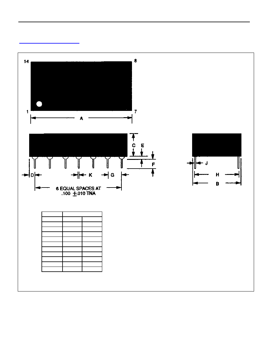
PKG 14-PIN
DIP
DIM MIN MAX
A IN
0.825
0.840
B IN
0.420
0.440
C IN
0.235
0.260
D IN
0.100
0.130
E IN
0.015
0.030
F IN
0.110
0.140
G IN
0.090
0.110
H IN
0.290
0.330
J IN
0.008
0.012
K IN
0.015
0.021
Note: Pins 2, 3 are missing by design.