 | –≠–ª–µ–∫—Ç—Ä–æ–Ω–Ω—ã–π –∫–æ–º–ø–æ–Ω–µ–Ω—Ç: DS4550 | –°–∫–∞—á–∞—Ç—å:  PDF PDF  ZIP ZIP |
General Description
The DS4550 is a 9-bit, nonvolatile (NV) I/O expander
with 64 bytes of NV user memory controlled by either
an I
2
C
TM
-compatible serial interface or an IEEE 1149.1
JTAG port. The DS4550 offers a digitally programmable
alternative to hardware jumpers and mechanical
switches that are being used to control digital logic
nodes. Each I/O pin is independently configurable. The
outputs are open drain with selectable pullups. Each
output has the ability to sink up to 16mA, and since the
device is NV, it powers up in the desired state allowing
it to control digital logic inputs immediately on power-
up without having to wait for the host CPU to initiate
control.
Applications
RAM-Based FPGA Bank Switching for Multiple
Profiles
Selecting Between Boot Flash
Setting ASIC Configurations/Profiles
Servers
Network Storage
Routers
Telecom Equipment
PC Peripherals
Features
Programmable Replacement for Mechanical
Jumpers and Switches
Nine NV Inputs/Outputs
64-Byte NV User Memory (EEPROM)
I
2
C-Compatible Serial Interface and JTAG
Up to 8 Devices can be Multidropped on the Same
I
2
C Bus
IEEE 1149.1 Boundary Scan Compliant
Open-Drain Outputs with Configurable Pullups
Outputs Capable of Sinking 16mA
Low Power Consumption
Wide Operating Voltage Range: 2.7V to 5.5V
Operating Temperature Range: -40∞C to +85∞C
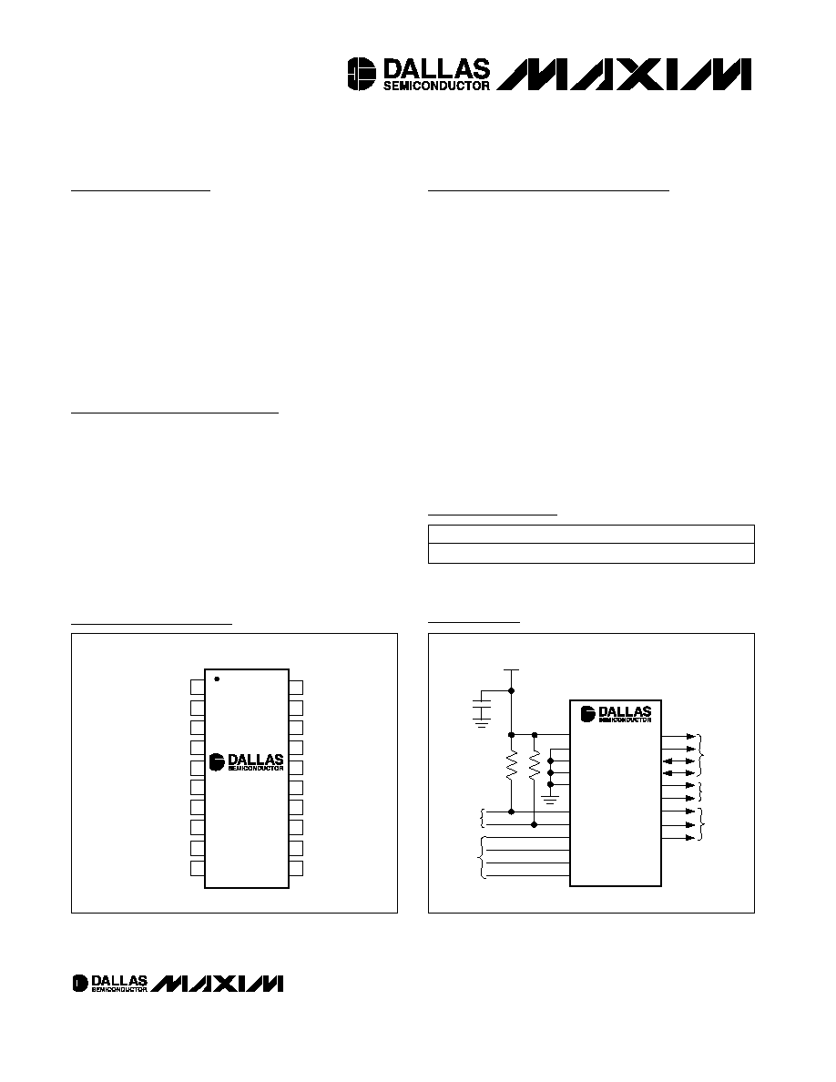
DS4550
I
2
C and JTAG Nonvolatile 9-Bit I/O
Expander Plus Memory
______________________________________________ Maxim Integrated Products
1
20
19
18
17
16
15
14
13
1
2
3
4
5
6
7
8
GND
I/O_8
I/O_7
I/O_6
I/O_3
I/O_2
I/O_1
I/O_0
TOP VIEW
I/O_5
A2
TDO
TDI
TCK
A1
A0
I/O_4
12
11
9
10
SCL
SDA
V
CC
TMS
TSSOP
DS4550
V
CC
FPGA
CLOCK
GENERATOR
CPU SPEED
SELECT
A0
A1
A2
GND
0.1µF
V
CC
4.7k
I
2
C
INTERFACE
JTAG
INTERFACE
DS4550
SCL
SDA
TCK
TMS
TDI
TDO
I/O_0
I/O_1
I/O_2
I/O_3
I/O_4
I/O_5
I/O_6
I/O_7
I/O_8
Pin Configuration
Typical Operating Circuit
Rev 0; 9/04
For pricing, delivery, and ordering information, please contact Maxim/Dallas Direct! at
1-888-629-4642, or visit Maxim's website at www.maxim-ic.com.
Ordering Information
PART
TEMP RANGE
PIN-PACKAGE
DS4550E
-40∞C to +85∞C
20 TSSOP
Add "/T&R" for tape and reel orders.
I
2
C is a trademark of Philips Corp. Purchase of I
2
C components from Maxim Integrated Products, Inc., or one of its sublicensed
Associated Companies, conveys a license under the Philips I
2
C Patent Rights to use these components in an I
2
C system, provided
that the system conforms to the I
2
C Standard Specification as defined by Philips.
DS4550
I
2
C and JTAG Nonvolatile 9-Bit I/O
Expander Plus Memory
2
_____________________________________________________________________
ABSOLUTE MAXIMUM RATINGS
RECOMMENDED OPERATING CONDITIONS
(T
A
= -40∞C to +85∞C)
Stresses beyond those listed under "Absolute Maximum Ratings" may cause permanent damage to the device. These are stress ratings only, and functional
operation of the device at these or any other conditions beyond those indicated in the operational sections of the specifications is not implied. Exposure to
absolute maximum rating conditions for extended periods may affect device reliability.
Voltage on V
CC
, SDA, and SCL Pins
Relative to Ground.............................................-0.5V to +6.0V
Voltage on A0, A1, A2, TCK, TMS, TDI, and I/O_n [n = 0 to 8]
Relative to Ground ...................................-0.5V to V
CC
+ 0.5V,
not to exceed +6.0V.
Operating Temperature Range ...........................-40∞C to +85∞C
EEPROM Programming Temperature Range .........0∞C to +70∞C
Storage Temperature Range .............................-55∞C to +125∞C
Soldering Temperature .....................See IPC/JEDEC J-STD-020
Specification
PARAMETER
SYMBOL
CONDITIONS
MIN
TYP
MAX
UNITS
Supply Voltage
V
CC
(Note 1)
+2.7
+5.5
V
Input Logic 1
V
IH
0.7 x
V
CC
V
CC
+
0.3
V
Input Logic 0
V
IL
-0.3
0.3 x
V
CC
V
DC ELECTRICAL CHARACTERISTICS
(V
CC
= +2.7V to +5.5V, T
A
= -40∞C to +85∞C, unless otherwise noted.)
PARAMETER
SYMBOL
CONDITIONS
MIN
TYP
MAX
UNITS
Standby Current
I
STBY
(Note 2)
2
10
µA
Input Leakage
I
L
-1.0
+1.0
µA
Input Current each I/O pin
I
I/O
0.4 < V
I/O
< 0.9 x V
CC
-1.0
+1.0
µA
3mA sink current
0.4
Low-Level Output Voltage (SDA)
V
OL SDA
6mA sink current
0.6
V
I/O Pins Low-Level Output
Voltage
V
OL I/O
16mA sink current
0.4
V
Low-Level Output Voltage (TDO)
V
OL TDO
4mA sink current
0.4
V
High-Level Output Voltage (TDO)
V
OH TDO
1mA source current
2.4
V
I/O Pin Pullup Resistors
R
PU
4.0
5.5
7.5
k
TMS, TDI Pullup Resistors
R
JPU
7.5
10
12.5
k
I/O Capacitance
C
I/O
(Note 3)
10
pF
Power-On Reset Voltage
V
POR
1.6
V
DS4550
I
2
C and JTAG Nonvolatile 9-Bit I/O
Expander Plus Memory
_____________________________________________________________________
3
AC ELECTRICAL CHARACTERISTICS-≠I
2
C Interface (See
Figure
5)
(V
CC
= +2.7V to +5.5V, T
A
= -40∞C to +85∞C, unless otherwise noted. Timing referenced to V
IL(MAX)
and V
IH(MIN)
.)
PARAMETER
SYMBOL
CONDITIONS
MIN
TYP
MAX
UNITS
SCL Clock Frequency
f
SCL
(Note 4)
0
400
kHz
Bus Free Time Between Stop and
Start Conditions
t
BUF
1.3
µs
Hold Time (Repeated) Start
Condition
t
HD:STA
(Note 5)
0.6
µs
Low Period of SCL
t
LOW
1.3
µs
High Period of SCL
t
HIGH
0.6
µs
Data Hold Time
t
HD:DAT
0
0.9
µs
Data Setup Time
t
SU:DAT
100
ns
Start Setup Time
t
SU:STA
0.6
µs
SDA and SCL Rise Time
t
R
(Note 6)
20 +
0.1C
B
300
ns
SDA and SCL Fall Time
t
F
(Note 6)
20 +
0.1C
B
300
ns
Stop Setup Time
t
SU:STO
0.6
µs
SDA and SCL Capacitive
Loading
C
B
(Note 6)
400
pF
EEPROM Write Time
t
WR
I
2
C EEPROM write (Note 7)
10
20
ms
AC ELECTRICAL CHARACTERISTICSJTAG Interface (See
Figure
1)
(V
CC
= +2.7V to +5.5V, T
A
= -40∞C to +85∞C, unless otherwise noted.)
PARAMETER
SYMBOL
CONDITIONS
MIN
TYP
MAX
UNITS
TCK Clock Period
t
1
1000
ns
TCK Clock High/Low Time
t
2
, t
3
(Note 8)
50
500
ns
TCK to TDI, TMS Setup Time
t
4
15
ns
TCK to TDI, TMS Hold Time
t
5
10
ns
TCK to TDO Delay
t
6
50
ns
TCK to TDO High-Z Delay
t
7
50
ns
EEPROM Write Time
t
WR
JTAG EEPROM write (Note 9)
10
20
ms
DS4550
I
2
C and JTAG Nonvolatile 9-Bit I/O
Expander Plus Memory
4
_____________________________________________________________________
NONVOLATILE MEMORY CHARACTERISTICS
(V
CC
= +2.7V to +5.5V, unless otherwise noted.)
PARAMETER
SYMBOL
CONDITIONS
MIN
TYP
MAX
UNITS
EEPROM Writes
+70∞C (Note 3)
50,000
Note 1: All voltages referenced to ground.
Note 2: I
STBY
is specified with SDA = SCL = TMS = TDI = V
CC
, outputs floating, and inputs connected to V
CC
or GND.
Note 3: Guaranteed by design.
Note 4: Timing shown is for fast-mode (400kHz) operation. This device is also backward-compatible with I
2
C standard mode timing.
Note 5: After this period, the first clock pulse is generated.
Note 6: C
B
total capacitance of one bus line in picofarads.
Note 7: EEPROM write time applies to all the EEPROM memory and SRAM-shadowed EEPROM memory when SEE = 0. The
EEPROM write time begins after a stop condition occurs.
Note 8: TCK can be stopped either high or low.
Note 9: EEPROM write begins immediately after the UPDATE-DR state that latches the data to be written. The EEPROM cannot be
accessed until the EEPROM write has completed. However, the remainder of the JTAG functionality is active and accessi-
ble during the EEPROM write.
TCK
t
1
t
2
t
3
t
4
t
5
t
6
t
7
TDI, TMS
TDO
Figure
1. JTAG Timing Diagram
DS4550
I
2
C and JTAG Nonvolatile 9-Bit I/O
Expander Plus Memory
_____________________________________________________________________
5
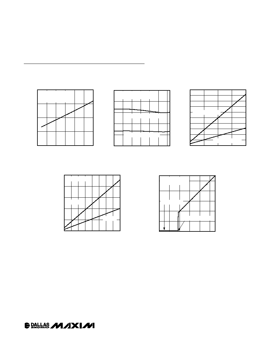
SUPPLY CURRENT
vs. SUPPLY VOLTAGE
DS4550 toc01
SUPPLY VOLTAGE (V)
SUPPLY CURRENT (
µ
A)
5
4.5
4
3.5
3
0.5
1
1.5
2
0
2.5
5.5
I/O0-I/O7 CONTROL BITS = 0
I/O0-I/O7 PULLUPS DISABLED
V
CC
= SDA = SCL = TCK
SUPPLY CURRENT
vs. TEMPERATURE
DS4550 toc02
TEMPERATURE (∞C)
SUPPLY CURRENT (
µ
A)
80
60
40
20
0
-20
0.5
1
1.5
2
2.5
0
-40
V
CC
= SDA = SCL = 5.5V = TCK
V
CC
= SDA = SCL = 2.7V = TCK
I/O0-I/O7 CONTROL BITS = 0
I/O0-I/O7 PULLUPS DISABLED
SUPPLY CURRENT
vs. SCL FREQUENCY
DS4550 toc03
SCL FREQUENCY (kHz)
SUPPLY CURRENT (
µ
A)
300
200
100
2
4
6
8
10
12
14
16
18
20
0
0
400
V
CC
= SDA = TCK = 5.0V
V
CC
= SDA = TCK = 2.7V
SUPPLY CURRENT
vs. TCK FREQUENCY
DS4550 toc04
TCK FREQUENCY (kHz)
SUPPLY CURRENT (
µ
A)
1750
1500
1250
1000
750
500
250
5
10
15
20
25
0
0
2000
V
CC
= 5.0V
V
CC
= 2.7V
SDA = SCL = V
CC
I/O OUTPUT VOLTAGE
vs. SUPPLY VOLTAGE
DS4550 toc05
SUPPLY VOLTAGE (V)
I/O OUTPUT VOLTAGE (V)
5
4
3
2
1
1
2
3
4
5
0
0
PULL-UPS ENABLED
PULL-DOWNS DISABLED
HIGH IMPEDANCE
EEPROM RECALL AT V
POR
Typical Operating Characteristics
(V
CC
= +5.0V, T
A
= +25∞C; TDI, TDO, TMS pins are no connects, unless otherwise noted.)

DS4550
I
2
C and JTAG Nonvolatile 9-Bit I/O
Expander Plus Memory
6
_____________________________________________________________________
Pin Description
PIN
NAME
FUNCTION
1
I/O_0
Input/Output 0. Bidirectional I/O pin.
2
I/O_1
Input/Output 1. Bidirectional I/O pin.
3
I/O_2
Input/Output 2. Bidirectional I/O pin.
4
I/O_3
Input/Output 3. Bidirectional I/O pin.
5
I/O_4
Input/Output 4. Bidirectional I/O pin.
6
A0
I
2
C Address Input. Inputs A0, A1, and A2 determine the I
2
C slave address of the device.
7
A1
I
2
C Address Input. Inputs A0, A1, and A2 determine the I
2
C slave address of the device.
8
TCK
JTAG Test Clock. This signal is used to shift data into TDI on the rising edge and out of TDO on the
falling edge.
9
TMS
JTAG Test Mode Select. This pin is sampled on the rising edge of TCK and used to place the TAP
into the various defined JTAG states. This pin has an internal pullup resistor.
10
V
CC
Power Supply Voltage
11
SDA
I
2
C Serial Data Open-Drain Input/Output
12
SCL
I
2
C Serial Clock Input
13
TDI
JTAG Test Data Input. Test instructions and data are clocked into this pin on the rising edge of TCK.
This pin has an internal pullup resistor.
14
TDO
JTAG Test Data Output. Test instructions and data are clocked out of this pin on the falling edge of
TCK. If not used, this pin should be left open circuit.
15
A2
I
2
C Address Input. Inputs A0, A1, and A2 determine the I
2
C slave address of the device.
16
I/O_5
Input/Output 5. Bidirectional I/O pin.
17
I/O_6
Input/Output 6. Bidirectional I/O pin.
18
I/O_7
Input/Output 7. Bidirectional I/O pin.
19
I/O_8
Input/Output 8. Bidirectional I/O pin.
20
GND
Ground
DS4550
I
2
C and JTAG Nonvolatile 9-Bit I/O
Expander Plus Memory
_____________________________________________________________________
7
I
2
C
INTERFACE
V
CC
SDA
SCL
A0
A1
A2
TMS
TDI
TDO
TCK
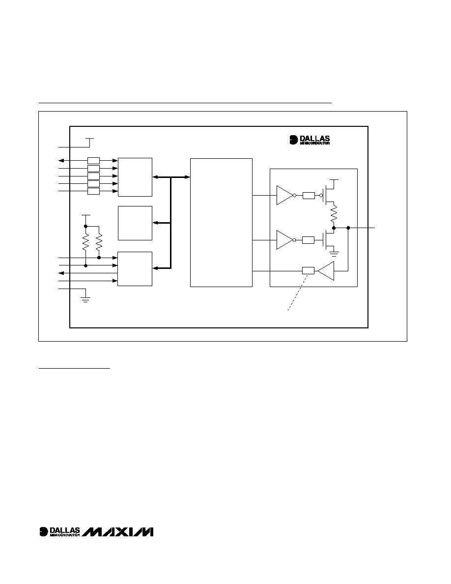
GND
DS4550
BSC
BSC
BSC
BSC
BSC
EEPROM
64 BYTES
USER
MEMORY
I/O CONTROL
REGISTERS
PULLUP ENABLE (F0h-F1h)
I/O CONTROL (F2h-F3h)
I/O STATUS (F8h-F9h)
BOUNDARY SCAN CELL (BSC)
JTAG
CONTROL
PORT
V
CC
V
CC
I/O CELL
(x9)
R
PU
I/O_n
[n = 0 TO 8]
V
CC
R
JPU
R
JPU
BSC
BSC
BSC
Block Diagram
Detailed Description
The DS4550 contains nine bidirectional, NV, input/out-
put (I/O) pins, and a 64-byte EEPROM user memory.
The I/O pins and user memory are accessible through
either the I
2
C compatible serial bus or the IEEE 1149.1
JTAG interface.
Programmable NV I/O Pins
Each programmable I/O pin consists of an input and an
open-collector output with a selectable internal pullup
resistor. To enable the pullups for each I/O pin, write to
the Pullup Enable Registers (F0h and F1h). To pull the
output low or place the pulldown transistor into a high-
impedance state, write to the I/O Control Registers (F2h
and F3h). To read the voltage levels present on the I/O
pins, read the I/O Status Registers (F8h and F9h). To
determine the status of the output register, read the I/O
Control Registers and the Pullup Resistor Registers.
The I/O Control Registers and the Pullup Enable
Registers are all SRAM-shadowed EEPROM registers.
It is possible to disable the EEPROM writes of the regis-
ters using the SEE bit in the Configuration Register.
This reduces the time required to write to the register
and increases the amount of times the I/O pins can be
adjusted before the EEPROM is worn out.
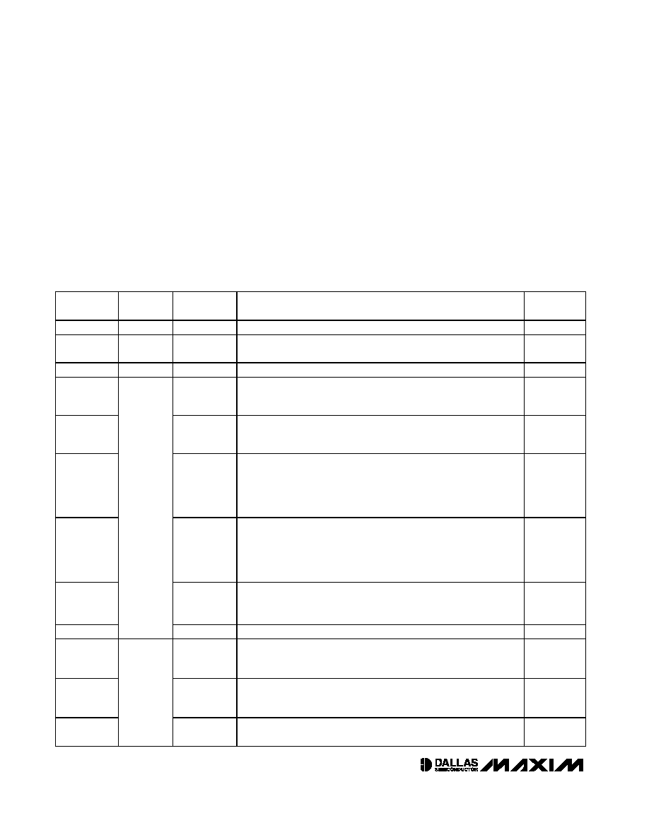
Memory Map and Memory Types
The DS4550 memory map is shown in
Table
1. Three
different types of memory are present in the DS4550:
EEPROM, SRAM-shadowed EEPROM, and SRAM.
Memory locations specified as EEPROM are NV.
Writing to these locations results in an EEPROM write
cycle for a time specified by t
WR
in the AC Electrical
Characteristics
table
. Locations specified as SRAM-
shadowed EEPROM can be configured to operate in
one of two modes specified by the SEE bit (the LSB of
the Configuration Register, F4h). When the SEE bit = 0
(default), the memory location acts like EEPROM.
However, when SEE = 1, shadow SRAM is written to
instead of the EEPROM. This eliminates both the EEP-
ROM write time, t
WR
, as well as the concern of wearing
out the EEPROM. This is ideal for applications that wish
to constantly write to the I/Os. Power-up default states
can be programmed for the I/Os in EEPROM (with SEE
= 0) and then once powered up, SEE can be written to
a 1 so that the I/Os can be updated periodically in
SRAM. The final type of memory present in the DS4550
is standard SRAM.
DS4550
I
2
C and JTAG Nonvolatile 9-Bit I/O
Expander Plus Memory
8
_____________________________________________________________________
ADDRESS
TYPE
NAME
FUNCTION
FACTORY
DEFAULT
00h to 3Fh
EEPROM
User Memory
64 Bytes of General-Purpose User EEPROM.
00h
40 to E7h
Reserved
Undefined Address Space for Future Expansion. Reads and writes to
this space will have no affect on the device.
E8 to EFh
EEPROM
Reserved
F0h
Pullup Enable
0
Pullup Enable for I/O_0 to I/O_7. I/O_0 is the LSB and I/O_7 is the
MSB. Set the corresponding bit to enable the pullup; clear the bit to
disable the pullup.
00h
F1h
Pullup Enable
1
Pullup Enable for I/O_8. I/O_8 is the LSB. Only the LSB is used. Set
the LSB bit to enable the pullup on I/O_8; clear the LSB to disable the
pullup.
00h
F2h
I/O Control 0
I/O Control for I/O_0 to I/O_7. I/O_0 is the LSB and I/O_7 is the MSB.
Clearing the corresponding bit of the register pulls the selected I/O
pin low; setting the bit places the pulldown transistor into a high-
impedance state. When the pulldown is high impedance, the output
will float if no pullup/down is connected to the pin.
FFh
F3h
I/O Control 1
I/O Control for I/O_8. I/O_8 is the LSB. Only the LSB is used. Clearing
the LSB of the register pulls the I/O_8 pin low; setting the LSB will
place the pulldown transistor into a high-impedance state. When the
pulldown is high impedance, the output will float if no pullup/down is
connected to the pin.
01h
F4h
Configuration
Configuration Register. The LSB is the SEE bit. When set, this bit
disables writes to the EEPROM; writing only effects the shadow
SRAM. When set to 0, both the EEPROM and the shadow SRAM is
written
00h
F5h to F7h
SRAM
Shadowed
EEPROM
[EEPROM
writes are
disabled if
the SEE bit
= 1]
User Memory
3 bytes of General-Purpose User EEPROM
00h
F8h
I/O Status 0
I/O Status for I/O_0 to I/O_7. I/O_0 is the LSB and I/O_7 is the MSB.
Writing to this register has no effect. Read this register to determine
the state of the I/O_0 to I/O_7 pins.
F9h
I/O Status 1
I/O Status for I/O_8. I/O_8 is the LSB. Only the LSB is used; the other
bits could be any value when read. Writing to this register has no
effect. Read this register to determine the state of the I/O_8 pin.
FAh to FFh
SRAM
SRAM User
Memory
6 Bytes of General-Purpose SRAM
Table
1. DS4550 Memory Map
Slave Address and Address Pins
The DS4550's I
2
C slave address is determined by the
state of the A0, A1, and A2 address pins as shown in
Figure
2. Address pins connected to GND result in a `0'
in the corresponding bit position in the slave address.
Conversely, address pins connected to V
CC
result in a
`1' in the corresponding bit positions. I
2
C communica-
tion is described in detail in a later section.
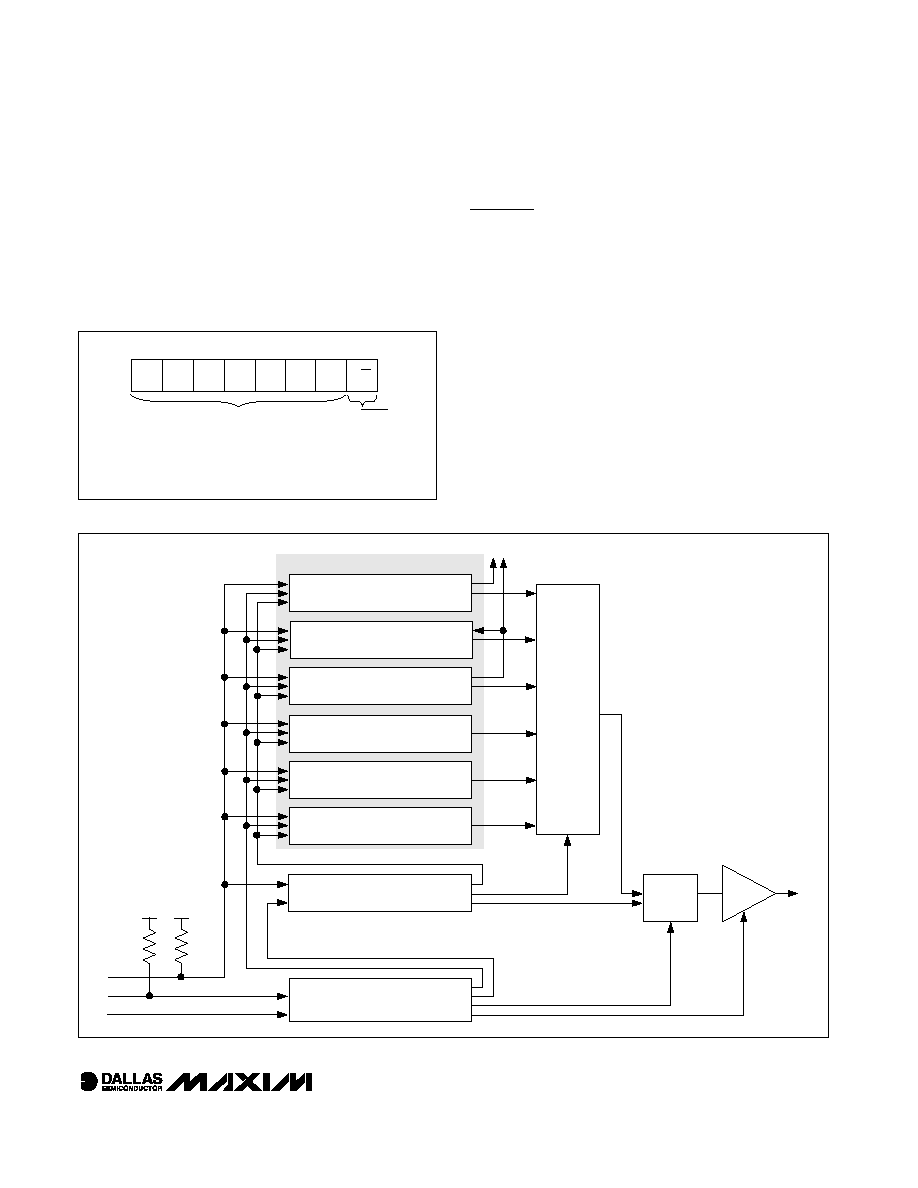
IEEE 1149.1 JTAG Operation
The DS4550 contains an IEEE 1149.1 compliant JTAG
port in addition to the I
2
C serial bus. Either can be used
to access the internal memory. However, the device
contains no bus arbitration and hence both busses
cannot be used at the same time. All of the I/O pins on
the DS4550 are IEEE 1149.1 boundary-scan compliant.
I/O_0 to I/O_8 as well as the I
2
C port pins, contain the
typical JTAG boundary scan cells, which allow the pins
to be polled or forced high/low using standard JTAG
instructions. The DS4550 also contains some exten-
sions to normal JTAG functionality, which allows access
to the internal memory. In particular, the DS4550 has
three device-specific test data registers (Memory
Address, Memory Read, and Memory Write) and three
device-specific instructions (ADDRESS, READ, and
WRITE), which provide memory access.
DS4550
I
2
C and JTAG Nonvolatile 9-Bit I/O
Expander Plus Memory
_____________________________________________________________________
9
MEMORY ADDRESS REGISTER
[LENGTH = 8 BITS]
MEMORY READ REGISTER
[LENGTH = 8 BITS]
MEMORY WRITE REGISTER
[LENGTH = 8 BITS]
MUX 1
LSB
MSB
TEST REGISTERS
EEPROM
TDO
MUX 2
BOUNDARY SCAN REGISTER
[LENGTH = 33 BITS]
IDENTIFICATION REGISTER
[LENGTH = 32 BITS]
V
CC
V
CC
MSB
R
JPU
R
JPU
TDI
TMS
TCK
LSB
BYPASS REGISTER
[LENGTH = 1 BIT]
INSTRUCTION REGISTER
[LENGTH = 4 BITS]
TEST ACCESS PORT
(TAP) CONTROLLER
Figure
3. DS4550 JTAG Block Diagram
*THE SLAVE ADDRESS IS DETERMINED BY
ADDRESS PINS A0, A1, AND A2.
1
MSB
SLAVE
ADDRESS*
READ/WRITE
BIT
LSB
0
1
0
A2
A1
A0
R/W
Figure
2. DS4550 I
2
C Slave Address Byte
DS4550
Test Access Port (TAP)
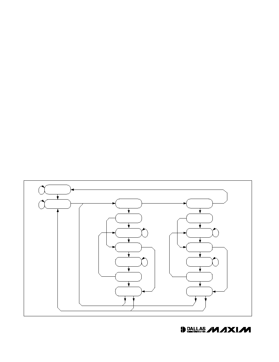
Controller State Machine
The TAP controller is a finite state machine that
responds to the logic level at TMS on the rising edge of
TCK (see
Figure
4).
Test-Logic-Reset. Upon power-up, the TAP controller
is in the Test-Logic-Reset state. The Instruction
Register contains the IDCODE instruction. All system
logic of the device operates normally.
Run-Test/Idle. The Run-Test/Idle state is used between
scan operations or during specific tests. The Instruction
Register and test data registers remain idle.
Select-DR-Scan. All test data registers retain their previ-
ous state. With TMS LOW, a rising edge of TCK moves
the controller into the Capture-DR state and initiates a
scan sequence. TMS HIGH during a rising edge on TCK
moves the controller to the Select-IR-Scan state.
Capture-DR. Data can be parallel-loaded into the test
data registers selected by the current instruction. If the
instruction does not call for a parallel load or the select-
ed test data register does not allow parallel loads, the
test data register remains at its current value. On the
rising edge of TCK, the controller goes to the Shift-DR
state if TMS is LOW or it goes to the Exit1-DR state if
TMS is HIGH.
Shift-DR. The test data register selected by the current
instruction is connected between TDI and TDO and
shifts data one stage toward its serial output on each
rising edge of TCK while TMS is LOW. On the rising
edge of TCK, the controller goes to the Exit1-DR state if
TMS is HIGH.
Exit1-DR. While in this state, a rising edge on TCK
puts the controller in the Update-DR state. A rising
edge on TCK with TMS LOW puts the controller in the
Pause-DR state.
Pause-DR. Shifting of the test data registers is halted
while in this state. All test data registers retain their pre-
vious state. The controller remains in this state while
TMS is LOW. A rising edge on TCK with TMS HIGH
puts the controller in the Exit2-DR state.
Exit2-DR. A rising edge on TCK with TMS HIGH while in
this state puts the controller in the Update-DR state. A ris-
ing edge on TCK with TMS LOW enters the Shift-DR state.
I
2
C and JTAG Nonvolatile 9-Bit I/O
Expander Plus Memory
10
____________________________________________________________________
Figure
4. TAP Controller State Diagram
TEST-LOGIC-RESET
1
1
1
1
0
0
RUN-TEST/IDLE
0
0
0
0
1
1
1
0
0
1
0
1
1
0
1
0
1
SELECT-DR-SCAN
SELECT-IR-SCAN
CAPTURE-DR
CAPTURE-IR
SHIFT-DR
SHIFT-IR
EXIT1-DR
EXIT1-IR
PAUSE-DR
PAUSE-IR
EXIT2-DR
EXIT2-IR
UPDATE-DR
UPDATE-IR
0
0
0
0
1
1
0
1
1
Update-DR. A falling edge on TCK while in the
Update-DR state latches the data from the shift regis-
ter path of the test data registers into a set of output
latches. This prevents changes at the parallel output
because of changes in the shift register. On the rising
edge of TCK, the controller goes to the Run-Test/Idle
state if TMS is LOW or it goes to the Select-DR-Scan
state if TMS is HIGH.
Select-IR-Scan. All test data registers retain their previ-
ous state. The Instruction Register remains unchanged
during this state. With TMS LOW, a rising edge on TCK
moves the controller into the Capture-IR state. TMS
HIGH during a rising edge on TCK puts the controller
back into the Test-Logic-Reset state.
Capture-IR. The Capture-IR state is used to load the
shift register in the Instruction Register with a fixed
value. This value is loaded on the rising edge of TCK. If
TMS is HIGH on the rising edge of TCK, the controller
enters the Exit1-IR state. If TMS is LOW on the rising
edge of TCK, the controller enters the Shift-IR state.
Shift-IR. In this state, the shift register in the Instruction
register is connected between TDI and TDO and shifts
data one stage for every rising edge of TCK toward the
TDO serial output while TMS is LOW. The parallel out-
puts of the Instruction Register as well as all test data
registers remain at their previous states. A rising edge
on TCK with TMS HIGH moves the controller to the
Exit1-IR state. A rising edge on TCK with TMS LOW
keeps the controller in the Shift-IR state while moving
data one stage through the Instruction Shift Register.
Exit1-IR. A rising edge on TCK with TMS LOW puts
the controller in the Pause-IR state. If TMS is HIGH on
the rising edge of TCK, the controller enters the
Update-IR state.
Pause-IR. Shifting of the Instruction shift register is halt-
ed temporarily. With TMS HIGH, a rising edge on TCK
puts the controller in the Exit2-IR state. The controller
remains in the Pause-IR state if TMS is LOW during a
rising edge on TCK.
Exit2-IR. A rising edge on TCK with TMS HIGH puts the
controller in the Update-IR state. The controller loops
back to Shift-IR if TMS is LOW during a rising edge of
TCK in this state.
Update-IR. The instruction code that has been shifted
into the Instruction shift register is latched to the paral-
lel outputs of the Instruction Register on the falling
edge of TCK as the controller enters this state. Once
latched, this instruction becomes the current instruc-
tion. A rising edge on TCK with TMS LOW puts the con-
troller in the Run-Test/Idle state. With TMS HIGH, the
controller enters the Select-DR-Scan state.
Instruction Register
The Instruction Register contains a shift register as well
as a latched parallel output and is 4 bits in length. When
the TAP controller enters the Shift-IR state, the Instruction
shift register is connected between TDI and TDO. While
in the Shift-IR state, a rising edge on TCK with TMS LOW
shifts the data one stage toward the serial output at TDO.
A rising edge on TCK in the Exit1-IR state or the Exit2-IR
state with TMS HIGH moves the controller to the Update-
IR state. The falling edge of that same TCK latches the
data in the Instruction shift register to the Instruction
Register parallel output. Instructions supported by the
DS4550 and its respective operational binary codes are
shown in
Table
2 below.
SAMPLE/PRELOAD. This is a mandatory instruction
for the IEEE 1149.1 specification that supports two
functions. The digital I/Os of the device can be sam-
pled at the Boundary Scan test data register without
interfering with the normal operation of the device by
using the Capture-DR state. SAMPLE/PRELOAD also
allows the device to shift data into the Boundary Scan
test data register through TDI using the Shift-DR state.
BYPASS. When the BYPASS instruction is latched into
the Instruction register, TDI connects to TDO through
the 1-bit Bypass test data register. This allows data to
pass from TDI to TDO without affecting the device's
normal operation.
EXTEST. This instruction allows testing of all intercon-
nections to the device. When the EXTEST instruction is
latched in the Instruction register, the following actions
occur. Once enabled through the Update-IR state, the
parallel outputs of all digital output pins are driven. The
Boundary Scan test data register is connected between
TDI and TDO. The Capture-DR samples all digital
inputs into the Boundary Scan test data register.
DS4550
I
2
C and JTAG Nonvolatile 9-Bit I/O
Expander Plus Memory
____________________________________________________________________
11
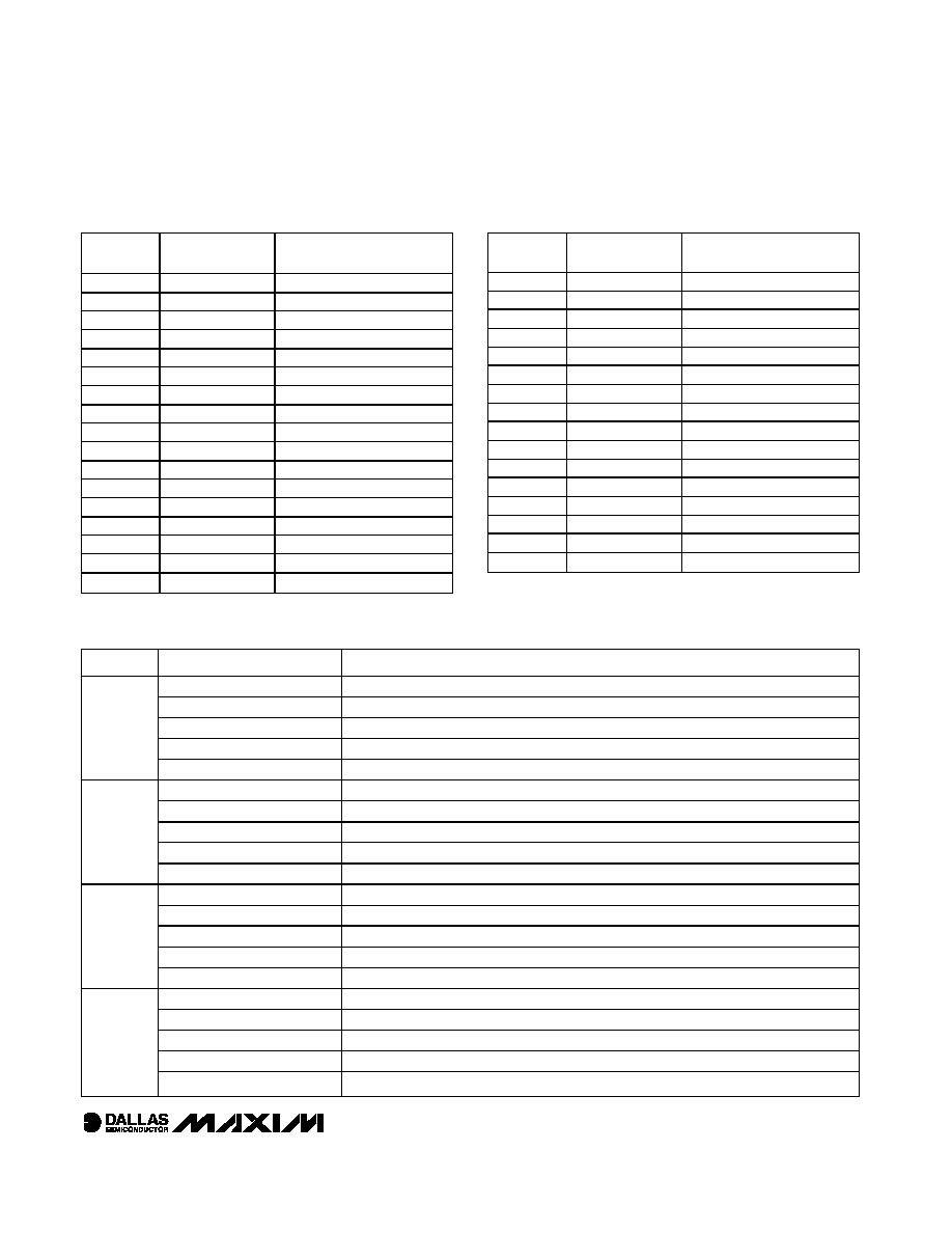
INSTRUCTION
SELECTED
REGISTER
INSTRUCTION
CODE
SAMPLE/PRELOAD
Boundary Scan
0010
BYPASS
Bypass
1111
EXTEST
Boundary Scan
0000
CLAMP
Bypass
0011
HIGHZ
Bypass
0100
IDCODE
Identification
0001
ADDRESS
Memory Address
1001
READ
Memory Read
1010
WRITE
Memory Write
1011
Table
2. Instruction Codes

DS4550
CLAMP. All digital outputs of the device output data
from the Boundary Scan parallel output while connect-
ing the Bypass test data register between TDI and
TDO. The outputs do not change during the CLAMP
instruction.
HIGHZ. All digital outputs of the device are placed in a
high-impedance state. The Bypass test data register is
connected between TDI and TDO.
IDCODE. When the IDCODE instruction is latched into
the parallel Instruction register, the Identification test
data register is selected. The device identification code
is loaded into the Identification test data register on the
rising edge of TCK following entry into the Capture-DR
state. Shift-DR can be used to shift the identification
code out serially through TDO. During Test-Logic-
Reset, the identification code is forced into the
Instruction register. The ID code always has a 1 in the
LSB position. The next 11 bits identify the manufactur-
er's JEDEC number and number of continuation bytes
followed by 16 bits for the device and 4 bits for the ver-
sion. See the diagram below.
ADDRESS. This is an extension to the standard IEEE
1149.1 instruction set to support access to the memory
in the DS4550. When the ADDRESS instruction is
latched into the Instruction register, TDI connects to
TDO through the 8-bit Memory Address test data regis-
ter during the Shift-DR state.
READ. This is an extension to the standard IEEE
1149.1 instruction set to support access to the memory
in the DS4550. When the READ instruction is latched
into the Instruction register, TDI connects to TDO
through the 8-bit Memory Read test data register dur-
ing the Shift-DR state.
WRITE. This is an extension to the standard IEEE
1149.1 instruction set to support access to the memory
in the DS4550. When the WRITE instruction is latched
into the Instruction register, TDI connects to TDO
through the 8-bit Memory Write test data register during
the Shift-DR state. When EEPROM writes occur using
the JTAG interface, the DS4550 will write the whole EEP-
ROM memory page (8 bytes) even though only a single
byte is modified. The unmodified bytes of the page are
transparently rewritten to their current values. The
DS4550's EEPROM write cycles are specified in the
Nonvolatile Memory Characteristics
table
. The specifica-
tion shown is at the worst-case temperature. It is capa-
ble of handling many more writes at room temperature.
Test Data Registers
IEEE 1149.1 requires a minimum of two test data regis-
ters; the Bypass Register and the Boundary Scan
Register. The optional Identification test data register
has been included in the DS4550 design along with
three DS4550 specific registers (Address, Read, Write)
to support access to the EEPROM.
Bypass Register. This is a one-bit shift register used in
conjunction with the BYPASS, CLAMP, and HIGHZ instruc-
tions. It provides a short path between TDI and TDO.
Boundary Scan Register. This register contains both a
shift register path and a latched parallel output for all
control cells and digital I/O cells. It is 33 bits in length.
See
Table
3 for the cell bit locations and definitions.
Identification Register. The Identification test data
register contains a 32-bit shift register and a 32-bit
latched parallel output. This register is selected during
the IDCODE instruction and when the TAP controller is
in the Test-Logic-Reset state.
Memory Address Register. This 8-bit register has a
latched parallel output that holds the memory address
location that is to be read from or written to. This regis-
ter is selected during the ADDRESS instruction.
Memory Read Register. This 8-bit load-only register
will latch the 8-bit value from the memory location indi-
cated by the address contained in the Address test
data register during the Capture-DR state. The data
can then be shifted out the TDO serial output by 8 ris-
ing edges of TCK during the Shift-DR state. See
Table
4 for a detailed example.
Memory Write Register. This 8-bit output-only register
will write its 8-bit value to the memory location indicated
by the address contained in the Address test data reg-
ister during the Update-DR state. The data is shifted
into the Write test data register through the TDI input
with 8 rising edges of TCK during the Shift-DR state
immediately prior to the Update-DR state. See
Table
5
for a detailed example.
I
2
C and JTAG Nonvolatile 9-Bit I/O
Expander Plus Memory
12
____________________________________________________________________
MSB LSB
Version (4 Bits)
Device ID (16 Bits)
Manufacturer ID (11 Bits)
Fixed Value (1 Bit)
0000
0001000000000000
00010100001
1
32-Bit ID Code
DS4550
I
2
C and JTAG Nonvolatile 9-Bit I/O
Expander Plus Memory
____________________________________________________________________
13
Table
3. Boundary Scan Control Bits [33 Bits]
CELL
NUMBER
NAME
TYPE
32
A2 input
Input Observe Only
31
A1 input
Input Observe Only
30
A0 input
Input Observe Only
29
SCL input
Input Observe Only
28
SDA input
Input Observe Only
27
SDA output
Output
26
IO8 pubout
Output
25
IO8 pdbout
Output
24
IO8 input
Input Observe Only
23
IO7 pubout
Output
22
IO7 pdbout
Output
21
IO7 input
Input Observe Only
20
IO6 pubout
Output
19
IO6 pdbout
Output
18
IO6 input
Input Observe Only
17
IO5 pubout
Output
16
IO5 pdbout
Output
Table
4. EEPROM Read Cycle
STEP
TAP STATE
COMMENTS
Select-IR-Scan
Capture-IR
Shift-IR (4 x TCK)
The 4-bit instruction is shifted in through TDI.
Exit1-IR
Select
Address
Register
Update-IR
Select-DR-Scan
Capture-DR
No-op.
Shift-DR (8 x TCK)
The 8-bit address is shifted in through TDI.
Exit1-DR
Load
EEPROM
Address
Update-DR
The shifted 8-bit Address Register data is output latched.
Select-IR-Scan
Capture-IR
Shift-IR (4 x TCK)
The 4-bit instruction is shifted in through TDI.
Exit1-IR
Select
Read
Register
Update-IR
Select-DR-Scan
Capture-DR
The 8-bit EEPROM data is loaded into the EEPROM Read Register.
Shift-DR (8 x TCK)
The 8-bit data is shifted out through TDO.
Exit1-DR
Read
EEPROM
Data
Update-DR
No-op.
CELL
NUMBER
NAME
TYPE
15
IO5 input
Input Observe Only
14
IO4 pubout
Output
13
IO4 pdbout
Output
12
IO4 input
Input Observe Only
11
IO3 pubout
Output
10
IO3 pdbout
Output
9
IO3 input
Input Observe Only
8
IO2 pubout
Output
7
IO2 pdbout
Output
6
IO2 input
Input Observe Only
5
IO1 pubout
Output
4
IO1 pdbout
Output
3
IO1 input
Input Observe Only
2
IO0 pubout
Output
1
IO0 pdbout
Output
0
IO0 input
Input Observe Only
DS4550
I
2
C and JTAG Nonvolatile 9-Bit I/O
Expander Plus Memory
14
____________________________________________________________________
Table
5. EEPROM Write Cycle
STEP
TAP STATE
COMMENTS
Select-IR-Scan
Capture-IR
Shift-IR (4 x TCK)
The 4-bit instruction is shifted in through TDI.
Exit1-IR
Select
Address
Register
Update-IR
Select-DR-Scan
Capture-DR
No-op.
Shift-DR (8 x TCK)
The 8-bit address is shifted in through TDI.
Exit1-DR
Load
EEPROM
Address
Update-DR
The shifted 8-bit Address Register data is output latched.
Select-IR-Scan
Capture-IR
Shift-IR (4 x TCK)
The 4-bit instruction is shifted in through TDI.
Exit1-IR
Select
Write
Register
Update-IR
Select-DR-Scan
Capture-DR
No-op.
Shift-DR (8 x TCK)
The 8-bit data is shifted in through TDI.
Exit1-DR
Write
EEPROM
Data
Update-DR
The shifted 8-bit EEPROM Write Register data is output latched and written to the
EEPROM.
I
2
C Serial Interface Description
I
2
C Definitions
The following terminology is commonly used to
describe I
2
C data transfers.
Master Device: The master device controls the slave
devices on the bus. The master device generates SCL
clock pulses, start and stop conditions.
Slave Devices: Slave devices send and receive data
at the master's request.
Bus Idle or Not Busy: Time between stop and start
conditions when both SDA and SCL are inactive and in
their logic high states. When the bus is idle it often initi-
ates a low-power mode for slave devices.
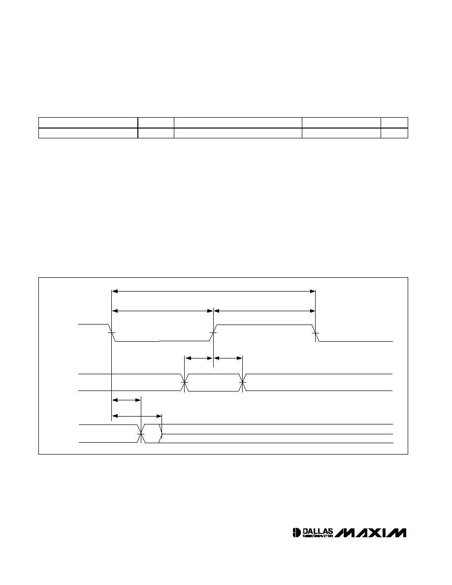
Start Condition: A start condition is generated by the
master to initiate a new data transfer with a slave.
Transitioning SDA from high to low while SCL remains
high generates a start condition. See the timing dia-
gram for applicable timing.
Stop Condition: A stop condition is generated by the
master to end a data transfer with a slave. Transitioning
SDA from low to high while SCL remains high gener-
ates a stop condition. See the timing diagram for
applicable timing.
Repeated Start Condition: The master can use a
repeated start condition at the end of one data transfer to
indicate that it will immediately initiate a new data trans-
fer following the current one. Repeated starts are com-
monly used during read operations to identify a specific
memory address to begin a data transfer. A repeated
start condition is issued identically to a normal start con-
dition. See the timing diagram for applicable timing.
Bit Write: Transitions of SDA must occur during the low
state of SCL. The data on SDA must remain valid and
unchanged during the entire high pulse of SCL plus the
setup and hold-time requirements (see
Figure
5). Data is
shifted into the device during the rising edge of the SCL.
Bit Read: At the end a write operation, the master must
release the SDA bus line for the proper amount of setup
time (see
Figure
5) before the next rising edge of SCL
during a bit read. The device shifts out each bit of data
on SDA at the falling edge of the previous SCL pulse
and the data bit is valid at the rising edge of the current
SCL pulse. Remember that the master generates all
SCL clock pulses including when it is reading bits from
the slave.
Acknowledgement (ACK and NACK):
An
Acknowledgement (ACK) or Not Acknowledge (NACK)
is always the 9th bit transmitted during a byte transfer.
The device receiving data (the master during a read or
the slave during a write operation) performs an ACK by
transmitting a zero during the 9th bit. A device per-
forms a NACK by transmitting a one during the 9th bit.
Timing (
Figure
5) for the ACK and NACK is identical to
all other bit writes. An ACK is the acknowledgment that
the device is properly receiving data. A NACK is used
to terminate a read sequence or as an indication that
the device is not receiving data.
Byte Write: A byte write consists of 8 bits of informa-
tion transferred from the master to the slave (most sig-
nificant bit first) plus a 1-bit acknowledgement from the
slave to the master. The 8-bits transmitted by the mas-
ter are done according to the bit write definition and the
acknowledgement is read using the bit read definition.
Byte Read: A byte read is an 8-bit information transfer
from the slave to the master plus a 1-bit ACK or NACK
from the master to the slave. The 8 bits of information
that are transferred (most significant bit first) from the
slave to the master are read by the master using the bit
read definition above, and the master transmits an ACK
using the bit write definition to receive additional data
bytes. The master must NACK the last byte read to ter-
minated communication so the slave returns control of
the SDA to the master.
Slave Address Byte: Each slave on the I
2
C bus
responds to a slave address byte sent immediately fol-
lowing a start condition. The slave address byte con-
tains the slave address in the most significant 7 bits
and the R/W bit in the least significant bit.
DS4550
I
2
C and JTAG Nonvolatile 9-Bit I/O
Expander Plus Memory
____________________________________________________________________
15
Figure
5. I
2
C Timing Diagram
SDA
SCL
t
HD:STA
t
LOW
t
HIGH
t
R
t
F
t
BUF
t
HD:DAT
t
SU:DAT
REPEATED
START
t
SU:STA
t
HD:STA
t
SU:STO
t
SP
STOP
START
NOTE: TIMING IS REFERENCED TO V
IL(MAX)
AND V
IH(MIN)

DS4550
The DS4550's slave address of the DS4550 is deter-
mined by the state of the A0, A1, and A2 address pins
as shown in
Figure
2. Address pins connected to GND
result in a `0' in the corresponding bit position in the
slave address. Conversely, address pins connected to
V
CC
result in a `1' in the corresponding bit positions.
When the R/W bit is 0 (such as in A0h), the master is
indicating it will write data to the slave. If R/W = 1, (A1h
in this case), the master is indicating it wants to read
from the slave.
If an incorrect slave address is written, the DS4550
assumes the master is communicating with another I
2
C
device and ignores the communication until the next
start condition is sent.
Memory Address: During an I
2
C write operation, the
master must transmit a memory address to identify the
memory location where the slave is to store the data.
The memory address is always the second byte trans-
mitted during a write operation following the slave
address byte.
I
2
C Communication
Writing a Single Byte to a Slave: The master must
generate a start condition, write the slave address byte
(R/W = 0), write the memory address, write the byte of
data, and generate a stop condition. Remember the
master must read the slave's acknowledgement during
all byte write operations.
Writing Multiple Bytes to a Slave: To write multiple
bytes to a slave, the master generates a start condition,
writes the slave address byte (R/W = 0), writes the
memory address, writes up to 8 data bytes, and gener-
ates a stop condition.
The DS4550 is capable of writing up to 8 bytes (1 page
or row) with a single I
2
C write transaction. This is inter-
nally controlled by an address counter that allows data
to be written to consecutive addresses without transmit-
ting a memory address before each data byte is sent.
The address counter limits the write to one 8-byte
page. Attempts to write to additional pages of memory
without sending a stop condition between pages
results in the address counter wrapping around to the
beginning of the present row. The first row begins at
address 00h and subsequent rows begin at multiples of
8 there on (08h, 10h, 18h, 20h, etc).
To prevent address wrapping from occurring, the mas-
ter must send a stop condition at the end of the page,
and then wait for the bus free or EEPROM write time to
elapse. Then the master can generate a new start con-
dition, write the slave address byte (R/W = 0), and the
first memory address of the next memory row before
continuing to write data.
Acknowledge Polling: Any time an EEPROM page is
written, the DS4550 requires the EEPROM write time
(t
WR
) after the stop condition to write the contents of the
page to EEPROM. During the EEPROM write time, the
device does not acknowledge its slave address
because it is busy. It is possible to take advantage of
this phenomenon by repeatedly addressing the
DS4550, which allows communication to continue as
soon as the DS4550 is ready. The alternative to
acknowledge polling is to wait for a maximum period of
t
WR
to elapse before attempting to access the device.
EEPROM Write Cycles: When EEPROM writes occur
using the I
2
C interface, the DS4550 writes the whole
EEPROM memory page even if only a single byte on a
page was modified. Writes that do not modify all 8
bytes on the page are valid and do not corrupt any
other bytes on the same page. Because the whole
page is written, even bytes on the page that were not
modified during the transaction are still subject to a
write cycle. The DS4550's EEPROM write cycles are
specified in the Nonvolatile Memory Characteristics
table
. The specification shown is at the worst-case tem-
perature. It is capable of handling many more writes at
room temperature.
Reading a Single Byte from a Slave: Unlike the write
operation that uses the specified memory address byte
to define where the data is to be written, the read oper-
ation occurs at the present value of the memory
address counter. To read a single byte from the slave,
the master generates a start condition, writes the slave
address byte with R/W = 1, reads the data byte with a
NACK to indicate the end of the transfer, and generates
a stop condition. However, since requiring the master
to keep track of the memory address counter is imprac-
tical, the following method should be used to perform
reads from a specified memory location.
Manipulating the Address Counter for Reads: A
dummy write cycle can be used to force the address
counter to a particular value. To do this, the master gen-
erates a start condition, writes the slave address byte
(R/W = 0), writes the memory address where it desires
to read, generates a repeated start condition, writes the
slave address byte (R/W = 1), reads data with ACK or
NACK as applicable, and generates a stop condition.
I
2
C and JTAG Nonvolatile 9-Bit I/O
Expander Plus Memory
16
____________________________________________________________________
See
Figure
6 for a read example using the repeated
start condition to specify the starting memory location.
Reading Multiple Bytes from a Slave: The read oper-
ation can be used to read multiple bytes with a single
transfer. When reading bytes from the slave, the master
simply ACKs the data byte if it desires to read another
byte before terminating the transaction. After the mas-
ter reads the last byte, it must NACK to indicate the end
of the transfer and generate a stop condition.
Applications Information
Power Supply Decoupling
To achieve best results, it is highly recommended that a
decoupling capacitor is used on the IC power-supply
pins. Typical values of decoupling capacitors are 0.01µF
and 0.1µF. Use a high-quality, ceramic, surface-mount
capacitor, and mount it as close as possible to the V
CC
and GND pins of the IC to minimize lead inductance.
DS4550
I
2
C and JTAG Nonvolatile 9-Bit I/O
Expander Plus Memory
____________________________________________________________________
17
Figure
6. I
2
C Communication Examples
SLAVE
ADDRESS*
START
START
1
0
1
0
A2
A1
A0
R/W
SLAVE
ACK
SLAVE
ACK
SLAVE
ACK
MSB
LSB
MSB
LSB
MSB
LSB
b7
b6
b5
b4
b3
b2
b1
b0
READ/
WRITE
REGISTER ADDRESS
b7
b6
b5
b4
b3
b2
b1
b0
DATA
STOP
SINGLE BYTE WRITE
-WRITE I/O CONTROL 0
REGISTER TO 00h
SINGLE BYTE WRITE
-WRITE PULLUP ENABLE 0
REGISTER TO FFh
SINGLE BYTE READ
-READ I/O STATUS 0 RESISTER
TWO BYTE WRITE
-WRITE I/O CONTROL 0 AND
I/O CONTROL 1 REGISTERS TO 00h
START
STOP
1 0 1 0 0 0 0 0
1 1 1 1 0 0 1 0
A0h
F2h
START
REPEATED
START
A1h
MASTER
NACK
STOP
1 0 1 0 0 0 0 0
1 1 1 1 1 0 0 0
F8h
1 0 1 0 0 0 0 1
1 0 1 0 0 0 0 0
1 1 1 1 0 0 1 0
A0h
F2h
STOP
I/O STATUS
START 1 0 1 0 0 0 0 0
1 1 1 1 0 0 0 0
A0h
F0h
STOP
DATA
FFh
00h
00h
EXAMPLE I
2
C TRANSACTIONS (WHEN A0, A1, AND A2 ARE CONNECTED TO GND)
TYPICAL I
2
C WRITE TRANSACTION
*THE SLAVE ADDRESS IS DETERMINED BY ADDRESS PINS A0, A1, AND A2.
0 0 0 0 0 0 0 0
1 1 1 1 1 1 1 1
A0h
0 0 0 0 0 0 0 0
TWO BYTE READ
-READ I/O STATUS 0 AND I/O
STATUS 1 RGISTERS
A)
C)
B)
D)
D)
START
STOP
1 0 1 0 0 0 0 0
1 1 1 1 1 0 0 0
A0h
F8h
A1h
1 0 1 0 0 0 0 1
I/O STATUS 0
DATA
I/O STATUS 1
DATA
SLAVE
ACK
SLAVE
ACK
SLAVE
ACK
SLAVE
ACK
SLAVE
ACK
SLAVE
ACK
SLAVE
ACK
SLAVE
ACK
SLAVE
ACK
SLAVE
ACK
SLAVE
ACK
SLAVE
ACK
SLAVE
ACK
SLAVE
ACK
SLAVE
ACK
SLAVE
ACK
MASTER
ACK
MASTER
NACK
REPEATED
START
0 0 0 0 0 0 0 0

DS4550
I
2
C and JTAG Nonvolatile 9-Bit I/O
Expander Plus Memory
Maxim cannot assume responsibility for use of any circuitry other than circuitry entirely embodied in a Maxim product. No circuit patent licenses are
implied. Maxim reserves the right to change the circuitry and specifications without notice at any time.
18 ____________________Maxim Integrated Products, 120 San Gabriel Drive, Sunnyvale, CA 94086 408-737-7600
© 2004 Maxim Integrated Products
Printed USA
is a registered trademark of Maxim Integrated Products.
is a registered trademark of Dallas Semiconductor Corporation.
Package Information
For the latest package outline information, go to
www.maxim-ic.com/DallasPackInfo
.
Chip Topology
TRANSISTOR COUNT: 21,161
SUBSTRATE CONNECTED TO GROUND