 | –≠–ª–µ–∫—Ç—Ä–æ–Ω–Ω—ã–π –∫–æ–º–ø–æ–Ω–µ–Ω—Ç: DS5000T | –°–∫–∞—á–∞—Ç—å:  PDF PDF  ZIP ZIP |
DS5000(T)
Soft Microcontroller Module
DS5000(T)
021998 1/19
FEATURES
∑
8≠bit 8051 compatible Microcontroller adapts to task≠
at≠hand:
≠ 8 or 32K bytes of nonvolatile RAM for program
and/or data memory storage
≠ Initial downloading of software in end system
via on≠chip serial port
≠ Capable of modifying its own program and/or
data memory in end use
∑
Crashproof operation:
≠ Maintains all nonvolatile resources for 10 years
in the absence of V
CC
≠ Power≠fail reset
≠ Early warning power≠fail interrupt
≠ Watchdog timer
∑
Software Security Feature:
≠ Executes encrypted software to prevent unau-
thorized disclosure
∑
On≠chip, full≠duplex serial I/O ports
∑
Two on≠chip timer/event counters
∑
32 parallel I/O lines
∑
Compatible with industry standard 8051 instruction
set and pinout
∑
Optional Permanently Powered Real≠Time Clock
(DS5000T)
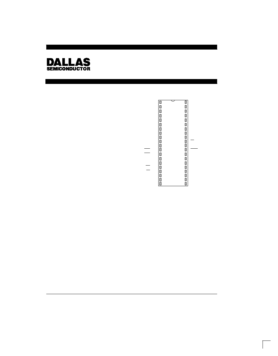
PIN ASSIGNMENT
1
2
3
4
5
6
7
8
9
10
11
12
13
14
15
16
17
18
19
20
21
22
23
24
40≠PIN ENCAPSULATED PACKAGE
25
26
27
28
29
30
31
32
33
34
35
36
37
38
39
40
P1.0
P1.1
P1.2
P1.3
P1.4
P1.5
P1.6
P1.7
RST
RXD P3.0
TXD P3.1
INT0 P3.2
INT1 P3.3
T0 P3.4
T1 P3.5
WR P3.6
RD P3.7
XTAL2
XTAL1
GND
V
CC
P0.0 AD0
P0.1 AD1
P0.2 AD2
P0.3 AD3
P0.4 AD4
P0.5 AD5
P0.6 AD6
P0.7 AD7
EA
ALE
PSEN
P2.7 A15
P2.6 A14
P2.5 A13
P2.4 A12
P2.3 A11
P2.2 A10
P2.1 A9
P2.0 A8
DESCRIPTION
The DS5000(T) Soft Microcontroller Module is a fully
8051 compatible 8≠bit CMOS microcontroller that offers
"softness" in all aspects of its application. This is ac-
complished through the comprehensive use of nonvola-
tile technology to preserve all information in the ab-
sence of system V
CC
. The internal program/data
memory space is implemented using either 8K or
32K bytes of nonvolatile CMOS SRAM. Furthermore,
internal data registers and key configuration registers
are also nonvolatile. An optional real time clock gives
permanently powered timekeeping. The clock keeps
time to a hundredth of a second using an on≠board
crystal.
DS5000(T)
021998 2/19
ORDERING INFORMATION
PART NUMBER
RAM SIZE
MAX CRYSTAL SPEED
TIMEKEEPING?
DS5000≠8≠16
8K bytes
16 MHz
No
DS5000≠32≠16
32K bytes
16 MHz
No
DS5000≠8≠16
8K bytes
16 MHz
Yes
DS5000T≠32≠16
32K bytes
16 MHz
Yes
Operating information is contained in the User's Guide section of the Secure Microcontroller Data Book. This data
sheet provides ordering information, pinout, and electrical specification.
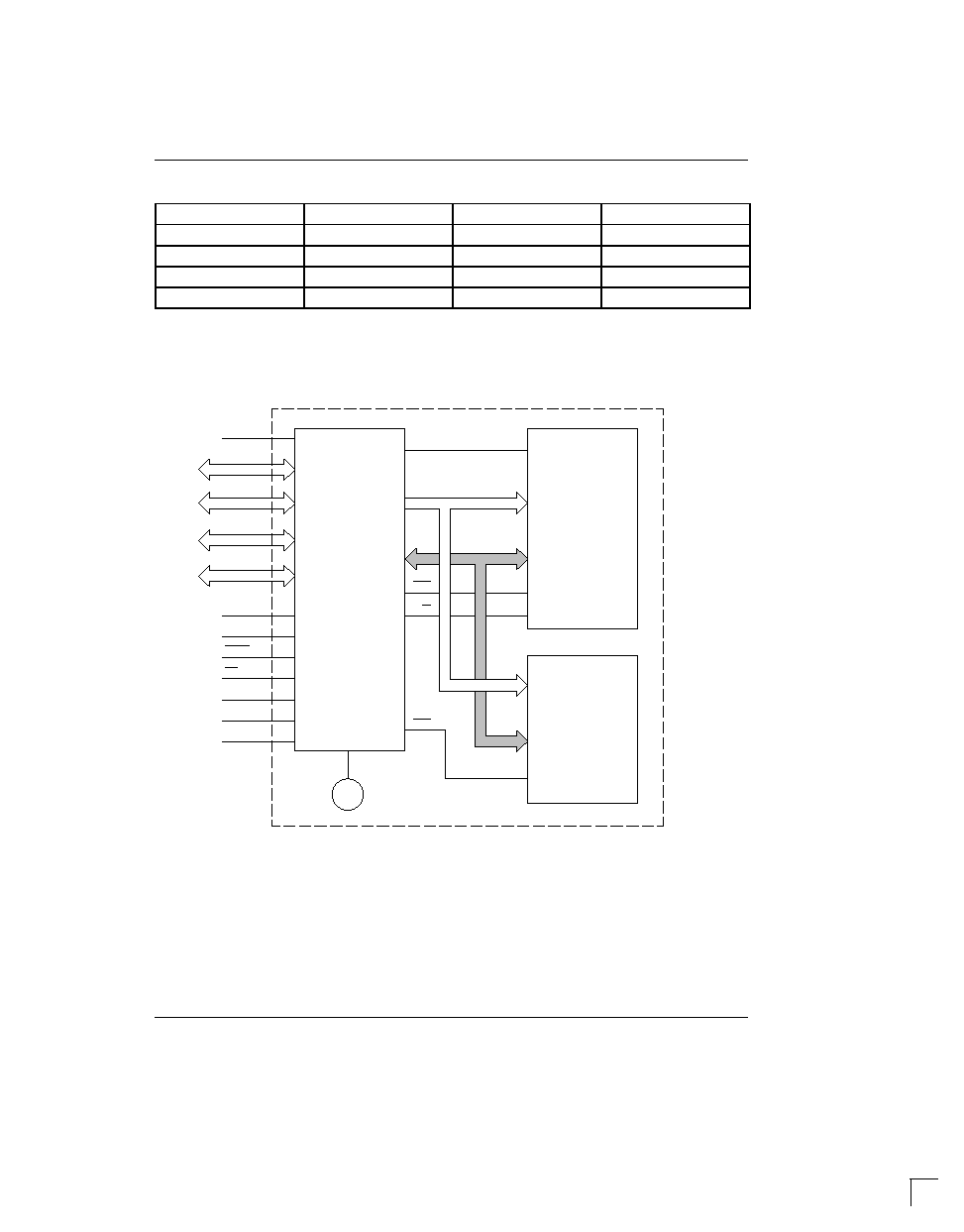
DS5000(T) BLOCK DIAGRAM Figure 1
ŒŒŒŒŒ
ŒŒŒŒŒ
ŒŒŒŒŒ
ŒŒŒŒŒ
ŒŒŒŒŒ
ŒŒŒŒŒ
ŒŒŒŒŒ
ŒŒŒŒŒ
P0.0≠0.7
P1.0≠1.7
P2.0≠2.7
P3.0≠3.7
RST
ALE
PSEN
EA
XTAL1
XTAL2
GND
V
CC
DS5000FP
ŒŒŒŒŒŒŒ
ŒŒŒŒŒŒŒ
ŒŒŒŒŒŒŒ
ŒŒŒŒŒŒŒ
ŒŒŒŒŒŒŒ
ŒŒŒŒŒŒŒ
ŒŒŒŒŒŒŒ
ŒŒŒŒŒŒŒ
ŒŒŒŒŒŒŒ
ŒŒŒŒŒŒŒ
V
CCO
CE1
R/W
CE2
BYTE≠WIDE
DATA BUS
BYTE≠WIDE
ADDRESS BUS
+3V
8K OR 32K
SRAM
(DS5000T)
REAL TIME
CLOCK
DS5000(T)
DS5000(T)
021998 3/19
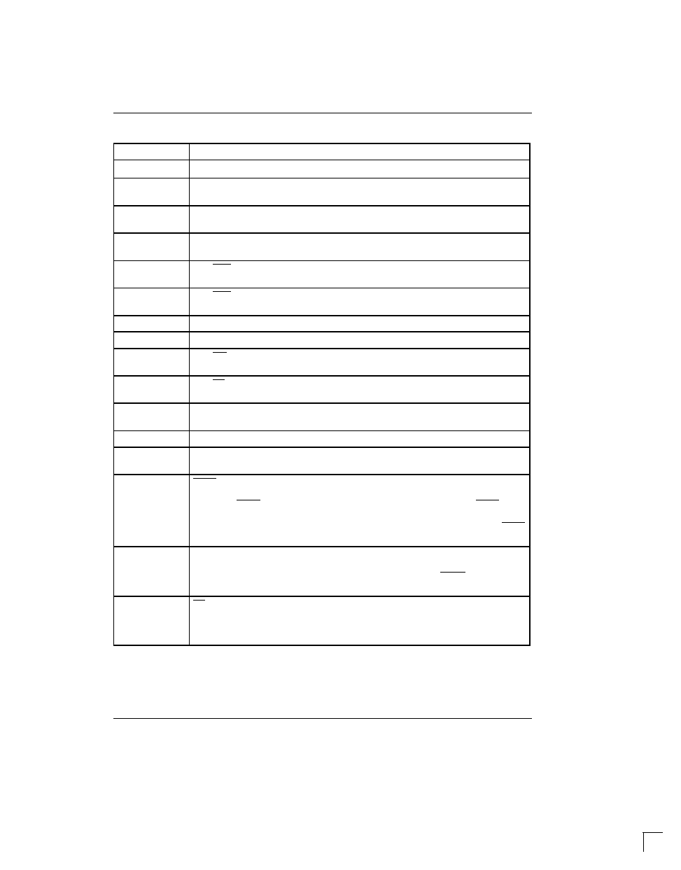
PIN DESCRIPTION
PIN NUMBER
DESCRIPTION
1≠8
P1.0 ≠ P1.7. General purpose I/O Port 1
1≠8
P1.0 ≠ P1.7. General purpose I/O Port 1.
9
RST ≠ Active high reset input. A logic 1 applied to this pin will activate a reset state. This pin
is pulled down internally so this pin can be left unconnected if not used.
10
P3.0 RXD. General purpose I/O port pin 3.0. Also serves as the receive signal for the on
board UART. This pin should not be connected directly to a PC COM port.
11
P3.1 TXD. General purpose I/O port pin 3.1. Also serves as the transmit signal for the on
board UART. This pin should not be connected directly to a PC COM port.
12
P3.2 INT0. General purpose I/O port pin 3.2. Also serves as the active low External
Interrupt 0.
13
P3.3 INT1. General purpose I/O port pin 3.3. Also serves as the active low External
Interrupt 1.
14
P3.4 T0. General purpose I/O port pin 3.4. Also serves as the Timer 0 input.
15
P3.5 T1. General purpose I/O port pin 3.5. Also serves as the Timer 1 input.
16
P3.6 WR. General purpose I/O port pin. Also serves as the write strobe for Expanded
bus operation.
17
P3.7 RD. General purpose I/O port pin. Also serves as the read strobe for Expanded bus
operation.
18, 19
XTAL2, XTAL1. Used to connect an external crystal to the internal oscillator. XTAL1 is the
input to an inverting amplifier and XTAL2 is the output.
20
GND. Logic ground.
21≠28
P2.0≠P2.7. General purpose I/O Port 2. Also serves as the MSB of the Expanded Address
bus.
29
PSEN ≠ Program Store Enable. This active low signal is used to enable an external program
memory when using the Expanded bus. It is normally an output and should be unconnected
if not used. PSEN also is used to invoke the Bootstrap Loader. At this time, PSEN will be
pulled down externally. This should only be done once the DS5000(T) is already in a reset
state. The device that pulls down should be open drain since it must not interfere with PSEN
under normal operation.
30
ALE ≠ Address Latch Enable. Used to de≠multiplex the multiplexed Expanded Address/Data
bus on Port 0. This pin is normally connected to the clock input on a '373 type transparent
latch. When using a parallel programmer, this pin also assumes the PROG function for pro-
gramming pulses.
31
EA ≠ External Access. This pin forces the DS5000(T) to behave like an 8031. No internal
memory (or clock) will be available when this pin is at a logic low. Since this pin is pulled down
internally, it should be connected to +5V to use NV RAM. In a parallel programmer, this pin
also serves as V
PP
for super voltage pulses.
DS5000(T)
021998 4/19
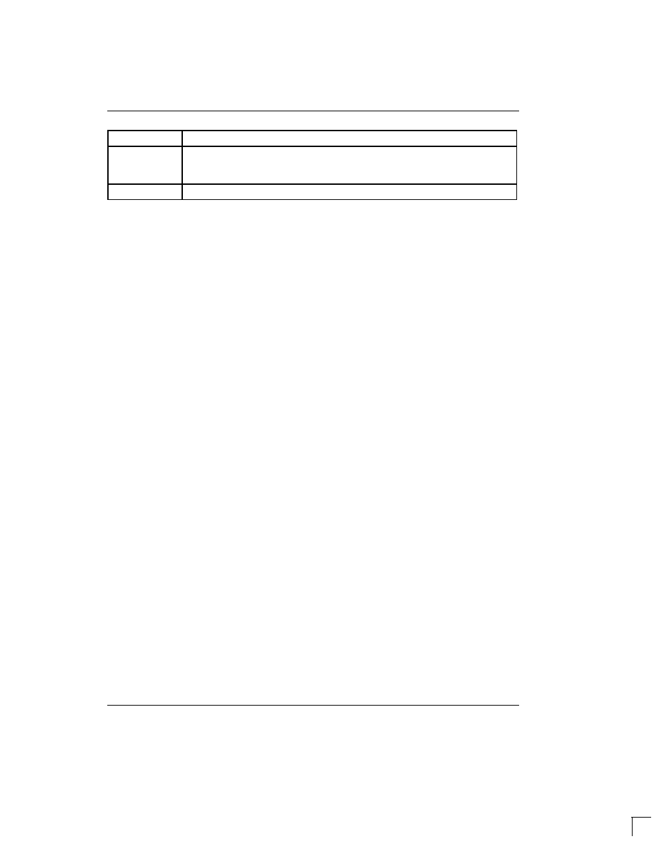
PIN NUMBER
DESCRIPTION
32≠39
P0.7≠P0.0. General purpose I/O Port 0. This port is open≠drain and can not drive a
logic 1. It requires external pull≠ups. Port 0 is also the multiplexed Expanded Address/Data
bus. When used in this mode, it does not require pull≠ups.
40
V
CC
≠ +5 volts.
INSTRUCTION SET
The DS5000(T) executes an instruction set which is ob-
ject code compatible with the industry standard 8051
microcontroller. As a result, software development
packages which have been written for the 8051 are
compatible with the DS5000(T), including cross≠as-
semblers, high≠level language compilers, and debug-
ging tools.
A complete description for the DS5000(T) instruction
set is available in the User's Guide section of the Secure
Microcontroller Data Book.
MEMORY ORGANIZATION
Figure 2 illustrates the address spaces which are ac-
cessed by the DS5000(T). As illustrated in the figure,
separate address spaces exist for program and data
memory. Since the basic addressing capability of the
machine is 16 bits, a maximum of 64K bytes of program
memory and 64K bytes of data memory can be ac-
cessed by the DS5000(T) CPU. The 8K or 32K byte
RAM area inside of the DS5000(T) can be used to con-
tain both program and data memory.
The Real time Clock (RTC) in the DS5000T is reached
in the memory map by setting a SFR bit. The MCON.2
bit (ECE2) is used to select an alternate data memory
map. While ECE2=1, all MOVXs will be routed to this
alternate memory map. The real time clock is a serial
device that resides in this area. A full description of the
RTC access and example software is given in the User's
Guide section of the Secure Microcontroller Data Book.
If the ECE2 bit is set on a DS5000 without a timekeeper,
the MOVXs will simply go to a nonexistent memory.
Software execution would not be affected otherwise.

DS5000(T)
021998 5/19
DS5000(T) LOGICAL ADDRESS SPACES Figure 2
ŒŒŒŒŒ
ŒŒŒŒŒ
ŒŒŒŒŒ
ŒŒŒŒŒ
ŒŒŒŒŒ
ŒŒŒŒŒ
ŒŒŒŒŒ
ŒŒŒŒŒ
ŒŒŒŒŒ
ŒŒŒŒŒ
ŒŒŒŒŒ
œœœœœ
œœœœœ
œœœœœ
œœœœœ
œœœœœ
œœœœœ
ŒŒŒŒŒ
ŒŒŒŒŒ
ŒŒŒŒŒ
ŒŒŒŒŒ
ŒŒŒŒŒ
ŒŒŒŒŒ
œœœœœ
œœœœœ
œœœœœ
œœœœœ
64K
32K
8K
œœ
œœ
ŒŒ
ŒŒ
NV RAM
PROGRAM
MEMORY
NV RAM
DATA
MEMORY
SPECIAL
FUNCTION
REGISTERS
DATA
REGISTERS
INTERNAL REGISTERS
LEGEND:
=
ON≠CHIP REGISTERS
=
ACCESSED VIA EXPANDED BUS
=
NV RAM MEMORY
PROGRAM
MEMORY
DATA
MEMORY
0
0
PARTITION
ADDR.
RANGE
ADDR.
127
0
255
128
≠
≠
≠
64K
32K
8K
≠
≠
≠
PROGRAM LOADING
The Program Load Modes allow initialization of the
NV RAM Program/Data Memory. This initialization may
be performed in one of two ways:
1. Serial Program Loading which is capable of per-
forming Bootstrap Loading of the DS5000(T). This
feature allows the loading of the application program
to be delayed until the DS5000(T) is installed in the
end system. Dallas Semiconductor strongly recom-
mends the use of serial program loading because of
its versatility and ease of use.
2. Parallel Program Load cycles which perform the ini-
tial loading from parallel address/data information
presented on the I/O port pins. This mode is timing≠
set compatible with the 8751H microcontroller pro-
gramming mode.
The DS5000(T) is placed in its Program Load configura-
tion by simultaneously applying a logic 1 to the RST pin
and forcing the PSEN line to a logic 0 level. Immediately
following this action, the DS5000(T) will look for a paral-
lel Program Load pulse, or a serial ASCII carriage return
(0DH) character received at 9600, 2400, 1200, or 300
bps over the serial port.
The hardware configurations used to select these
modes of operation are illustrated in Figure 3.