1 of 50
061499
FEATURES
ß
87C52-Compatible
-
8051 pin- and instruction set-compatible
-
Three 16-bit timer/counters
-
256 bytes scratchpad RAM
ß
On-chip Memory
-
8 kbytes EPROM (OTP & Windowed Packages)
-
1 kbyte extra on-chip SRAM for MOVX access
ß
On-
chip Analog to Digital Converter
-
Eight channels of analog input, 10-bit resolution
-
Fast conversion time
-
Selectable internal or external reference voltage
ß
Pulse Width Modulator Outputs
-
Four channels of 8-bit PWM
-
Channels cascadable to 16-bit PWM
ß
4 Capture + 3 Compare Registers
ß
55 I/O Port Pins
ß
New Dual Data Pointer Operation
-
Either data pointer can be incremented or
decremented
ß
ROMSIZE Feature
-
Selects effective on-chip ROM size from 0 to 8k
-
Allows access to entire external memory map
-
Dynamically adjustable by software
ß
High-Speed Architecture
-
4 clocks/machine cycle (8051 = 12)
-
Runs DC to 33 MHz clock rates
-
Single-cycle instruction in 121 ns
-
New Stretch Cycle feature allows access to
fast/slow memory or peripherals
ß
Unique Power Savings Modes
ß
EMI Reduction Mode disables ALE when not
needed
ß
High integration controller includes:
-
Power-fail reset
-
Early-warning power-fail interrupt
-
Two full-duplex hardware serial ports
-
Programmable watchdog timer
ß
16 total interrupt sources with 6 external
Available in 68-pin PLCC, 80-pin PQFP, and
68-pin windowed CLCC
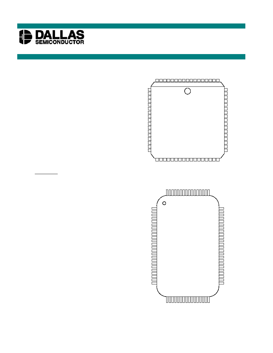
PIN ASSIGNMENT
DS87C550
EPROM High-Speed
Micro with A/D and PWM
PRODUCT PREVIEW
www.dalsemi.com
9
1
61
27
43
10
26
60
44
68-Pin PLCC
68-Pin WINDOWED CLCC
DALLAS
DS87C550
1
24
64
41
40
25
65
80
DALLAS
DS87C550
80-Pin PQFP

DS87C550
2 of 50
DESCRIPTION
The DS87C550 EPROM High-Speed Micro with A/D and PWM is a member of the fastest 100% 8051-
compatible microcontroller family available. It features a redesigned processor core that removes wasted
clock and memory cycles. As a result, it executes 8051 instructions up to three times faster than the
original architecture for the same crystal speed. The DS87C550 also offers a maximum crystal speed of
33 MHz, resulting in apparent execution speeds of up to 99 MHz.
The DS87C550 uses an industry standard 8051 pin-out and includes standard resources such as three
timer/counters, and 256 bytes of scratchpad RAM. This device also features 8 kbytes of EPROM with an
extra 1 kbyte of data RAM (in addition to the 256 bytes of scratchpad RAM), and 55 I/O ports pins. Both
One-Time-Programmable (OTP) and windowed packages are available.
Besides greater speed, the DS87C550 includes a second full hardware serial port, seven additional
interrupts, a programmable watchdog timer, brownout monitor, and power-fail reset.
The DS87C550 also provides dual data pointers (DPTRs) to speed block data memory moves. The user
can also dynamically adjust the speed of external accesses between two and 12 machine cycles for
flexibility in selecting memory and peripherals.
Power Management Mode (PMM) is useful for portable or battery-powered applications. This feature
allows software to select a lower speed clock as the main time base. While normal operation has a
machine cycle rate of 4 clocks per cycle, the PMM allows the processor to run at 1024 clocks per cycle.
For example, at 12 MHz, standard operation has a machine cycle rate of 3 MHz. In Power Management
Mode, software can select an 11.7 kHz (12 MHz/1024) machine cycle rate. There is a corresponding
reduction in power consumption due to the processor running slower.
The DS87C550 also offers two features that can significantly reduce electromagnetic interference (EMI).
One EMI reduction feature allows software to select a reduced emission mode that disables the ALE
signal when it is unneeded. The other EMI reduction feature controls the current to the address and data
pins interfacing to external devices producing a controlled transition of these signals.
ORDERING INFORMATION
PART NUMBER
PACKAGE
MAX. CLOCK SPEED
TEMPERATURE RANGE
DS87C550-QCL
68-pin PLCC
33 MHz
0∞C to +70∞C
DS87C550-FCL
80-pin PQFP
33 MHz
0∞C to +70∞C
DS87C550-QNL
68-pin PLCC
33 MHz
-40∞C to +85∞C
DS87C550-FNL
80-pin PQFP
33 MHz
-40∞C to +85∞C
DS87C550-KCL
68-pin windowed CLCC
33 MHz
0∞C to 70∞C
DS87C550
3 of 50
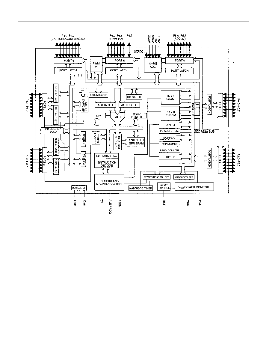
DS87C550 BLOCK DIAGRAM Figure 1

DS87C550
4 of 50
PIN DESCRIPTION Table 1
PLCC/
CLCC
QFP
SIGNAL NAME
DESCRIPTION
2
72
V
CC
V
CC
- Digital +5V power input.
36
37
34
35
GND
GND ≠ Digital ground.
15
9
RST
RST - I/O. The RST input pin contains a Schmitt voltage input to recognize
external active high Reset inputs. The pin also employs an internal pulldown
resistor to allow for a combination of wired OR external Reset sources. An RC is
not required for power-up, as the DS87C550 provides this function internally.
This pin also acts as an output when the source of the reset is internal to the device
(i.e., watchdog timer, power-fail, or crystal-fail detect). In this case, the RST pin
will be held high while the processor is in a Reset state, and will return to low as
the processor exits this state. When this output capability is used, the RST pin
should not be connected to an RC network or a logic output driver.
35
34
32
31
XTAL1
XTAL2
Input - The crystal oscillator pins XTAL1 and XTAL2 provide support for
fundamental mode, parallel resonant, AT cut crystals. XTAL1 acts also as an input
if there is an external clock source in place of a crystal. XTAL2 serves as the
output of the crystal amplifier. Note that this output cannot be used to drive any
additional load when a crystal is attached as this can disturb the oscillator circuit.
47
48
PSEN
PSEN
- Output. The Program Store Enable output. This signal is commonly
connected to optional external ROM memory as a chip enable.
PSEN
will provide
an active low pulse during a program byte access, and is driven high when not
accessing external program memory.
48
49
ALE
ALE - Output. The Address Latch Enable output functions as a clock to latch the
external address LSB from the multiplexed address/data bus on Port 0. This signal
is commonly connected to the latch enable of an external 373 family transparent
latch. ALE is driven high when the DS87C550 is in a Reset condition. ALE can
also be disabled and forced high using the EMI reduction mode ALEOFF.
49
50
EA
EA
- Input. An active low input pin that when connected to ground will force the
DS87C550 to use an external program memory. The internal RAM is still
accessible as determined by register settings.
EA
should be connected to V
CC
to
use internal program memory. The input level on this pin is latched at reset.
16-23
10-17
P1.0-P1.7
Port 1 - I/O. Port 1 functions as both an 8-bit, bi-directional I/O port and an
alternate functional interface for several internal resources. The reset condition of
Port 1 is all bits at logic 1. In this state, a weak pullup holds the port high. This
condition allows the pins to serve as both input and output. Input is possible since
any external circuit whose output drives the port will overcome the weak pullup.
When software writes a 0 to any Port 1 pin, the DS87C550 will activate a strong
pulldown that remains on until either a 1 is written or a reset occurs. Writing a 1
after the port has been at 0 will cause a strong transition driver to turn on, followed
by a weaker sustaining pullup. Once the momentary strong driver turns off, the
port again returns to a weakly held high output (and input) state. The alternate
functions of Port 1 pins are detailed below. Note that when the Capture/Compare
functions of timer 2 are used, the interrupt input pins become capture trigger
inputs.
Port
Alternate Function
16
10
P1.0
INT2/CT0 External Interrupt 2/Capture Trigger 0
17
11
P1.1
INT3/CT1 External Interrupt 3/Capture Trigger 1
18
12
P1.2
INT4/CT2 External Interrupt 4/Capture Trigger 2
19
13
P1.3
INT5/CT3 External Interrupt 5/Capture Trigger 3
20
14
P1.4
T2
External I/O for Timer/Counter 2
21
15
P1.5
T2EX
Timer/Counter 2 Capture/Reload Trigger
22
16
P1.6
RXD1
Serial Port 1 Input
23
17
P1.7
TXD1
Serial Port 1 Output
DS87C550
5 of 50
PLCC/
CLCC
QFP
SIGNAL NAME
DESCRIPTION
50-57
57
56
55
54
53
52
51
50
51-58
58
57
56
55
54
53
52
51
P0.0 (AD0)
P0.1 (AD1)
P0.2 (AD2)
P0.3 (AD3)
P0.4 (AD4)
P0.5 (AD5)
P0.6 (AD6)
P0.7 (AD7)
Port 0-I/O - AD0-7. Port 0 is an open-drain 8-bit, bi-directional general-purpose
I/O port. When used in this mode pullup resistors are required to provide a logic 1
output. As an alternate function, Port 0 operates as a multiplexed address/data bus
to access off-chip memory or peripherals. In this mode, the LSB of the memory
address is output on the bus during the time that ALE is high. When ALE falls to
a logic 0, the port transitions to a bi-directional data bus. In this mode, the port
provides active high drivers for logic 1 output. The reset condition of Port 0 is tri-
state (i.e., the open drain devices are off).
39-46
39
40
41
42
43
44
45
46
38-42
45-47
38
39
40
41
42
45
46
47
P2.0 (A8)
P2.1 (A9)
P2.2 (A10)
P2.3 (A11)
P2.4 (A12)
P2.5 (A13)
P2.6 (A14)
P2.7 (A15)
Port 2-I/O Address A15:A8. Port 2 functions as an 8-bit bi-directional I/O port
or alternately as an external address bus (A15-A8). The reset condition of Port 2 is
logic high I/O state. In this state, weak pullups hold the port high allowing the
pins to be used as an input or output as described above for Port 1. As an alternate
function Port 2 can function as MSB of the external address bus. This bus can be
used to read external memory or peripherals.
24-31
18-20
23-27
P3.0-P3.7
Port 3 - I/O. Port 3 functions as an 8-bit bi-directional I/O port or alternately as
an interface for External Interrupts, Serial Port 0, Timer 0 & 1 Inputs, and
RD
and
WR
strobes. When functioning as an I/O port, these pins operate as indicated
above for Port 1. The alternate modes of Port 3 are detailed below.
Port
Alternate Mode
24
18
P3.0
RXD0
Serial Port 0 Input
25
19
P3.1
TXD0
Serial Port 0 Output
26
20
P3.2
INT0
External Interrupt 0
27
23
P3.3
INT1
External Interrupt 1
28
24
P3.4
T0
Timer 0 External Input
29
25
P3.5
T1
Timer 1 External Input
30
26
P3.6
WR
External Data Memory Write Strobe
31
27
P3.7
RD
External Data Memory Read Strobe
7-14
80
1-2
4-8
P4.0-P4.7
Port 4 - I/O. Port 4 functions as an 8-bit bi-directional I/O port or alternately as
an interface to Timer 2's Capture Compare functions. When functioning as an I/O
port, these pins operate as indicated in the Port 1 description. The alternate modes
of Port 4 are detailed below.
Port 4 Alternate Mode
7
80
P4.0
CMSR0
Timer 2 compare match set/reset output 0
8
1
P4.1
CMSR1
Timer 2 compare match set/reset output 1
9
2
P4.2
CMSR2
Timer 2 compare match set/reset output 2
10
4
P4.3
CMSR3
Timer 2 compare match set/reset output 3
11
5
P4.4
CMSR4
Timer 2 compare match set/reset output 4
12
6
P4.5
CMSR5
Timer 2 compare match set/reset output 5
13
7
P4.6
CMT0
Timer 2 compare match toggle output 0
14
8
P4.7
CMT1
Timer 2 compare match toggle output 1