General Description
The MAX9812/MAX9813 are single/dual-input, 20dB
fixed-gain microphone amplifiers. They offer tiny pack-
aging and a low-noise, integrated microphone bias,
making them ideal for portable audio applications such
as notebook computers, cell phones, and PDAs. These
amplifiers feature a 500kHz bandwidth, Rail-to-RailÆ
outputs, an industry-leading 100dB power-supply rejec-
tion ratio, and a very low 0.015% THD+N. Power-saving
features include very low 230µA supply current and a
total shutdown mode that cuts the combined supply
and BIAS currents to only 100nA.
The MAX9812 is a single amplifier in a 6-pin SC70
package (2mm x 2.1mm) and the MAX9813 is a dual-
input amplifier available in an 8-pin SOT23 (3mm x
3mm) package. The MAX9813 has two inputs allowing
two microphones to be multiplexed to a single output.
The MAX9812/MAX9813 are offered in two grades. The
MAX9812L/MAX9813L are optimized for 3.3V supply
operation (2.7V to 3.6V). The MAX9812H/MAX9813H are
PC2001 compliant and are optimized for 5V operation
(4.5V to 5.5V). Both devices are specified over the -40∞C
to +85∞C extended operating temperature range.
Applications
Notebook Computers
PDAs
Smart Phones
Car Kit Adapters
Digital Cameras
Video Tape Recorders
Features
o PC2001 Compliant
o 100dB at 217Hz Power-Supply Rejection Ratio
o Very Low 230µA Quiescent Current
o Low 0.015% THD+N
o Available in Two Versions
MAX9812L/MAX9813L--2.7V to 3.6V
MAX9812H/MAX9813H--4.5V to 5.5V
o Internal Low-Noise Microphone Bias Supply
2.3V for MAX9812L/MAX9813L
4.0V for MAX9812H/MAX9813H
o 100nA Low-Power Shutdown Mode
o Rail-to-Rail Outputs
o 20dB Fixed Gain
o Available in Tiny 6-Pin SC70 (2mm x 2.1mm) and
8-Pin SOT23 (3mm x 3mm) Packages
o Extended Temperature Range -40∞C to +85∞C
MAX9812/MAX9813
Tiny, Low-Cost, Single/Dual-Input, Fixed-Gain
Microphone Amplifiers with Integrated Bias
________________________________________________________________ Maxim Integrated Products
1
Ordering Information
19-2840; Rev 0; 4/03
For pricing, delivery, and ordering information, please contact Maxim/Dallas Direct! at
1-888-629-4642, or visit Maxim's website at www.maxim-ic.com.
Pin Configurations, Selector Guide, and Typical Operating
Circuits appear at end of data sheet.
PART
TEMP RANGE
PIN-
PACKAGE
V
CC
(V)
MAX9812LEXT-T
-40
∞C to +85∞C 6 SC70-6
2.7 to 3.6
MAX9812HEXT-T
-40
∞C to +85∞C 6 SC70-6
4.5 to 5.5
MAX9813LEKA-T
-40
∞C to +85∞C 8 SOT23-8
2.7 to 3.6
MAX9813HEKA-T
-40
∞C to +85∞C 8 SOT23-8
4.5 to 5.5
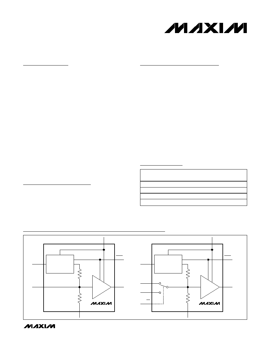
MAX9812
20dB
REFERENCE
2.3V (L VERSION)
4.0V (H VERSION)
IN
BIAS
OUT
SHDN
V
CC
GND
MAX9813
20dB
IN1/IN2
REFERENCE
2.3V (L VERSION)
4.0V (H VERSION)
IN2
IN1
BIAS
OUT
SHDN
V
CC
GND
Simplified Block Diagrams
Rail-to-Rail is a trademark of Nippon Motorola Ltd.
MAX9812/MAX9813
Tiny, Low-Cost, Single/Dual-Input, Fixed-Gain
Microphone Amplifiers with Integrated Bias
2
_______________________________________________________________________________________
ABSOLUTE MAXIMUM RATINGS
ELECTRICAL CHARACTERISTICS
(V
CC
= 3.3V, I
BIAS
= 500µA (MAX9812L/MAX9813L), V
CC
= 5V, I
BIAS
= 800µA (MAX9812H/MAX9813H), GND = 0V, R
L
= open,
SHDN = V
CC
, T
A
= T
MIN
to T
MAX
, unless otherwise noted. Typical values are at T
A
= +25
∞C.) (Note 1)
Stresses beyond those listed under "Absolute Maximum Ratings" may cause permanent damage to the device. These are stress ratings only, and functional
operation of the device at these or any other conditions beyond those indicated in the operational sections of the specifications is not implied. Exposure to
absolute maximum rating conditions for extended periods may affect device reliability.
(All voltages referenced to GND)
V
CC
........................................................................-0.3V to +6.0V
All Other Pins..............................................-0.3V to (V
CC
+ 0.3V)
Continuous Current (IN, SHDN, IN1, IN2, IN1/IN2)...........
±20mA
OUT, BIAS Short-Circuit Duration (to GND or V
CC
) ...Continuous
Continuous Power Dissipation (T
A
= +70
∞C)
6-Pin SC70 (derate 3.1mW/
∞C above +70∞C)..............245mW
8-Pin SOT23 (derate 8.9mw/
∞C above +70∞C) ............714mW
Operating Temperature Range ...........................-40
∞C to +85∞C
Storage Temperature Range .............................-65
∞C to +150∞C
Junction Temperature ......................................................+150
∞C
Lead Temperature (soldering, 10s) .................................+300
∞C
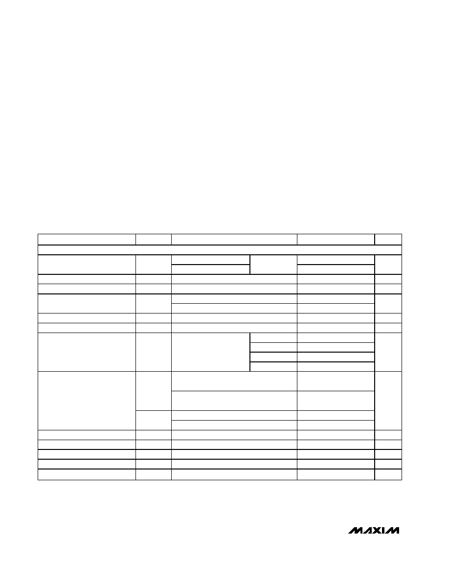
PARAMETER
SYMBOL
CONDITIONS
MIN
TYP
MAX
UNITS
GENERAL
MAX9812L/MAX9813L
2.7
3.6
Supply Voltage Range
V
CC
MAX9812H/MAX9813H
Inferred from
PSRR test
4.5
5.5
V
Supply Current
I
CC
I
BIAS
= 0
230
400
µA
Shutdown Supply Current
I
CC_SHDN
SHDN = GND
0.1
1
µA
MAX9812L/MAX9813L
1.35
1.5
1.65
Amplifier Output Bias Voltage
V
OUT_DC
MAX9812H/MAX9813H
2.25
2.5
2.75
V
Input Resistance
R
IN
85
k
Voltage Gain
A
V
19
20
21
dB
DC
90
100
f = 217Hz
100
f = 1kHz
100
Power-Supply Rejection Ratio
PSRR
OUT
Input referred, T
A
= +25∞C
f = 10kHz
90
dB
R
L
= 10k
to V
CC
/2
V
CC
-
0.1
V
OH
R
L
= 1k
to V
CC
/2
V
CC
-
0.25V
V
CC
-
0.1V
R
L
= 10k
to V
CC
/2
0.1
Output Voltage Swing
V
OL
R
L
= 1k
to V
CC
/2
0.1
0.25
V
Output Short-Circuit Current
I
OUT_SC
Sinking or sourcing
3
12
24
mA
Small-Signal -3dB Bandwidth
BW
V
OUT
= 10mV
P-P
400
kHz
Output Capacitive-Load Stability
C
L
No sustained oscillations
50
pF
Output Impedance
Z
OUT
f = 1kHz
0.5
Output Slew Rate
SR
V
OUT
= 1V step
1
V/µs
MAX9812/MAX9813
Tiny, Low-Cost, Single/Dual-Input, Fixed-Gain
Microphone Amplifiers with Integrated Bias
_______________________________________________________________________________________
3
ELECTRICAL CHARACTERISTICS (continued)
(V
CC
= 3.3V, I
BIAS
= 500µA (MAX9812L/MAX9813L), V
CC
= 5V, I
BIAS
= 800µA (MAX9812H/MAX9813H), GND = 0V, R
L
= open,
SHDN = V
CC
, T
A
= T
MIN
to T
MAX
, unless otherwise noted. Typical values are at T
A
= +25
∞C.) (Note 1)
Note 1: All specifications are 100% tested at T
A
= +25∞C. Temperature limits are guaranteed by design.
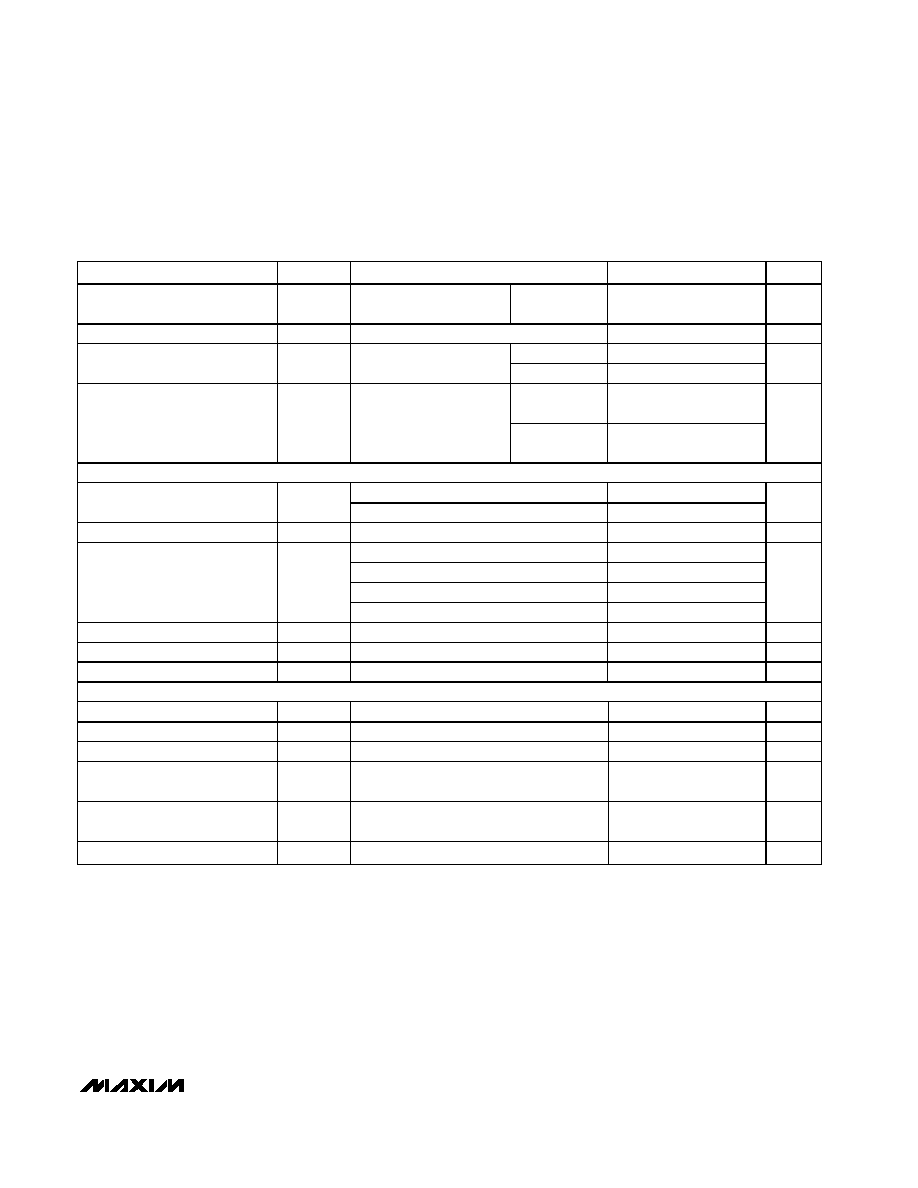
PARAMETER
SYMBOL
CONDITIONS
MIN
TYP
MAX
UNITS
Amplifier Input Voltage-Noise
Density
e
n
Inputs at AC GND
f = 1kHz
40
nV/
Hz
Total Integrated Input Noise
V
n
22Hz to 22kHz BW, inputs at AC GND
5
µV
RMS
1kHz
75
Off-Isolation
Input referred, MAX9813
only
10kHz
60
dB
VOUT = 1V
P-P
(L version)
0.04
Total Harmonic Distortion Plus
Noise
THD+N
f = 1kHz, R
L
= 10k
to
V
CC
/2, BW = 22Hz to
22kHz
VOUT = 4V
P-P
(H version)
0.015
%
BIAS
MAX9812L/MAX9813L
2.1
2.30
2.55
Bias Output Voltage Range
V
BIAS
MAX9812H/MAX9813H
3.6
4.0
4.4
V
Bias Output Resistance
R
BIAS
0.1
DC, T
A
= +25∞C
70
80
f = 217Hz
80
f = 1kHz
75
Power-Supply Rejection Ratio
(V
CC
to BIAS)
PSRR
BIAS
f = 10kHz
55
dB
BIAS Current Limit
I
BIAS_SC
BIAS short to GND
5
22
50
mA
BIAS Capacitive-Load Stability
C
BIAS
No sustained oscillations
50
pF
Total Integrated BIAS Noise
V
n
22Hz to 22kHz BW
29
µV
RMS
DIGITAL INPUTS (
SHDN, IN1/IN2)
Logic-Low Threshold
V
IL
0.8
V
Logic-High Threshold
V
IH
2.0
V
Logic Input Current
I
IN
SHDN = GND or V
CC
±1
µA
Shutdown Enable Time
t
SHDN_ON
95% of settled value
10
ms
Shutdown Disable Time
t
SHDN_OFF
50
µs
IN1/IN2 Select Time
t
SEL
10
µs
MAX9812/MAX9813
Tiny, Low-Cost, Single/Dual-Input, Fixed-Gain
Microphone Amplifiers with Integrated Bias
4
_______________________________________________________________________________________
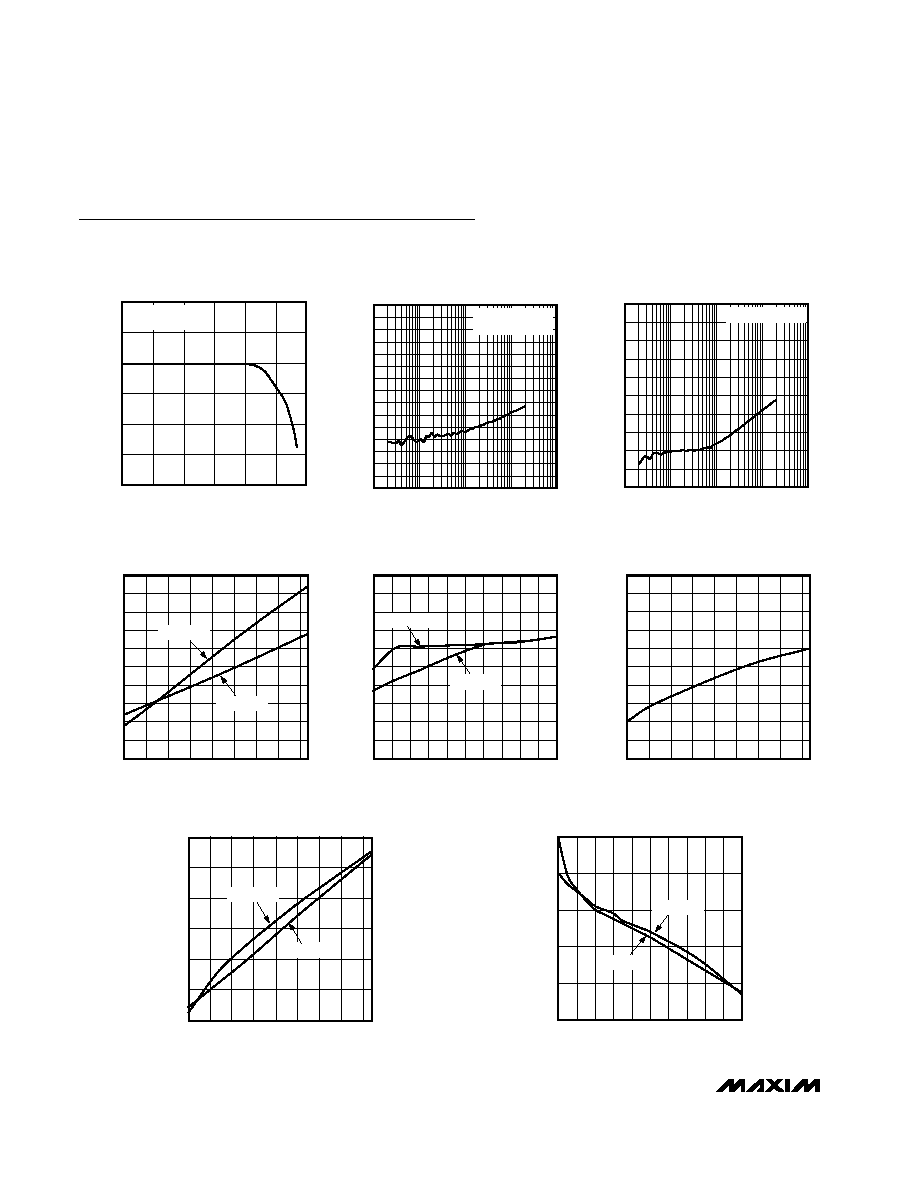
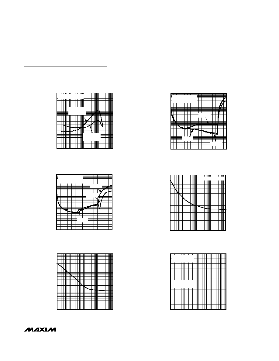
Typical Operating Characteristics
(V
CC
= 3.3V (MAX9812L/MAX9813L), V
CC
= 5V (MAX9812H/MAX9813H), GND = 0V, R
L
= 10k
to V
CC
/2, SHDN = V
CC
, T
A
= +25
∞C,
unless otherwise noted.)
-20
0
-10
20
10
30
40
10
1k
10k
100
100k
1M
10M
GAIN vs. FREQUENCY
MAX9812 toc01
FREQUENCY (Hz)
OUTPUT VOLTAGE GAIN (dB)
R
L
= OPEN
V
OUT
= 10mV
P-P
POWER-SUPPLY REJECTION RATIO
vs. FREQUENCY
MAX9812 toc02
FREQUENCY (Hz)
PSRR (dB)
10k
1k
100
10
100k
-150
-80
-90
-100
-110
-120
-130
-140
-60
-70
-40
-50
-30
-10
-20
0
V
RIPPLE
= 200mV
P-P
INPUT REFERRED
POWER-SUPPLY REJECTION RATIO
(V
CC
TO BIAS) vs. FREQUENCY
MAX9812 toc03
FREQUENCY (Hz)
PSRR (V
CC
TO BIAS) (dB)
10k
1k
100
-90
-80
-70
-60
-50
-40
-30
-20
-10
0
-100
10
100k
V
RIPPLE
= 200mV
P-P
200
210
205
220
215
230
225
235
245
240
250
-40
-10
5
20
-25
35
50
65
80
SUPPLY CURRENT
vs. TEMPERATURE
MAX9812 toc04
TEMPERATURE (
∞C)
SUPPLY CURRENT (
µ
A)
MAX9812H
MAX9812L
100
140
120
180
160
220
200
240
280
260
300
2.0
2.8 3.2 3.6
2.4
4.0 4.4 4.8
5.6
5.2
6.0
SUPPLY CURRENT
vs. SUPPLY VOLTAGE
MAX9812 toc05
SUPPLY VOLTAGE (V)
SUPPLY CURRENT (
µ
A)
MAX9812L
MAX9812H
0.05
0.07
0.06
0.09
0.08
0.11
0.10
0.12
0.14
0.13
0.15
-40
-10
5
20
-25
35
50
65
80
SHUTDOWN SUPPLY CURRENT
vs. TEMPERATURE
MAX9812 toc06
TEMPERATURE (
∞C)
SHUTDOWN SUPPLY CURRENT (
µ
A)
2.27
2.28
2.29
2.30
2.31
2.32
2.33
-40
-10
-25
5
20
35
50
65
80
V
BIAS
vs. TEMPERATURE
MAX9812 toc07
TEMPERATURE (
∞C)
V
BIAS
(L VERSION) (V)
3.97
3.98
3.99
4.00
4.01
4.02
4.03
3.96
V
BIAS
(H VERSION) (V)
MAX9812H
MAX9812L
2.2997
2.2998
2.2999
2.3000
2.3001
2.3002
0
0.8 1.0
0.4 0.6
0.2
1.2 1.4 1.6 1.8 2.0
V
BIAS
vs. I
BIAS
MAX9812 toc08
I
BIAS
(mA)
V
BIAS
(L VERSION) (V)
MAX9812H
MAX9812L
3.9998
3.9999
4.0000
4.0001
4.0002
V
BIAS
(H VERSION) (V)
MAX9812/MAX9813
Tiny, Low-Cost, Single/Dual-Input, Fixed-Gain
Microphone Amplifiers with Integrated Bias
_______________________________________________________________________________________
5
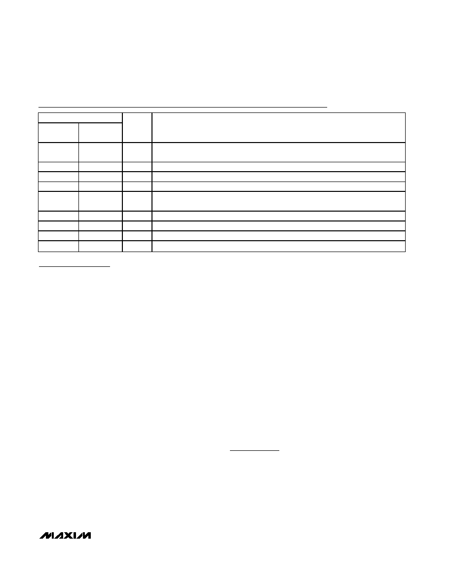
TOTAL HARMONIC DISTORTION PLUS NOISE
vs. OUTPUT AMPLITUDE
MAX9812 toc10
OUTPUT AMPLITUDE (V
RMS
)
THD+N (%)
1.8
1.6
1.4
1.2
1.0
0.8
0.6
0.4
0.2
0.01
0.1
1
10
0.001
0
2.0
H VERSION
BW = 22Hz TO 22kHz
f = 10kHz
f = 1kHz
f = 100Hz
TOTAL HARMONIC DISTORTION PLUS NOISE
vs. OUTPUT AMPLITUDE
MAX9812 toc11
OUTPUT AMPLITUDE (V
RMS
)
THD+N (%)
1.0
0.5
0.01
0.1
1
100
10
0.001
0
1.5
f = 10kHz
f = 100Hz
f = 1kHz
L VERSION
BW = 22Hz TO 22kHz
100
50
30
70
10
10
10k
100k
FREQUENCY (Hz)
INPUT-REFERRED NOISE (nV/
Hz
)
100
INPUT-REFERRED NOISE vs. FREQUENCY
INPUTS AT AC GND
1k
MAX9812 toc12
BIAS NOISE vs. FREQUENCY
MAX9812 toc13
FREQUENCY (Hz)
BIAS NOISE (nV/
Hz
)
10k
1k
100
100
1000
10,000
10
10
100k
OFF-ISOLATION vs. FREQUENCY
MAX9812 toc14
FREQUENCY (Hz)
CROSSTALK (dB)
10k
1k
100
-90
-80
-70
-60
-50
-40
-30
-20
-10
0
10
-100
10
100k
MAX9813
V
IN1
= 100mV
RMS
IN1 TO OUT WITH
IN2 SELECTED
Typical Operating Characteristics (continued)
(V
CC
= 3.3V (MAX9812L/MAX9813L), V
CC
= 5V (MAX9812H/MAX9813H), GND = 0V, R
L
= 10k
to V
CC
/2, SHDN = V
CC
, T
A
= +25
∞C,
unless otherwise noted.)
TOTAL HARMONIC DISTORTION PLUS NOISE
vs. FREQUENCY
MAX9812 toc09
FREQUENCY (Hz)
THD+N (%)
10k
1k
100
0.01
0.1
1
0.001
10
100k
V
OUT
= 1V
RMS
R
L
= 2k
BW = 22Hz TO 22kHz
V
OUT
= 1V
RMS
R
L
= 10k

MAX9812/MAX9813
Tiny, Low-Cost, Single/Dual-Input, Fixed-Gain
Microphone Amplifiers with Integrated Bias
6
_______________________________________________________________________________________
2
µs/div
OUTPUT OVERDRIVEN
OUT
1V/div
MAX9812 toc19
IN
500mV/div
Typical Operating Characteristics (continued)
(V
CC
= 3.3V (MAX9812L/MAX9813L), V
CC
= 5V (MAX9812H/MAX9813H), GND = 0V, R
L
= 10k
to V
CC
/2, SHDN = V
CC
, T
A
= +25
∞C,
unless otherwise noted.)
1ms/div
OUT-OF-SHUTDOWN WAVEFORM
INPUT FLOATING
MAX9812 toc17
OUT
2V/div
BIAS
2V/div
SHDN
2V/div
100
µs/div
MAX9813
SWITCHING BETWEEN TWO INPUTS
1V/div
MAX9812 toc18
2V/div
OUT
IN1/IN2
IN2 = 200mV
P-P
AT 20kHz
IN1 = 100mV
P-P
AT 10kHz
1
µs/div
SMALL-SIGNAL PULSE RESPONSE
(R
L
= OPEN, C
L
= 10pF)
IN
5mV/div
MAX9812 toc15
OUT
50mV/div
2
µs/div
LARGE-SIGNAL PULSE RESPONSE
(R
L
= OPEN, C
L
= 10pF)
IN
100mV/div
MAX9812 toc16
OUT
1V/div
0V
MAX9812/MAX9813
Tiny, Low-Cost, Single/Dual-Input, Fixed-Gain
Microphone Amplifiers with Integrated Bias
_______________________________________________________________________________________
7
Pin Description
Detailed Description
The MAX9812_/MAX9813_ are low-power fixed-gain
microphone amplifiers available in a single- or dual-
input configuration. The gain is set at 10V/V (20dB) with
a 400kHz, -3dB bandwidth. They also feature a low-
noise, integrated microphone input bias voltage.
Single/Dual Input
The MAX9812L/MAX9812H are single-input amplifiers
and the MAX9813L/MAX9813H are dual-input ampli-
fiers. All devices typically have an input impedance of
85k
. The inputs to the dual version are controlled
through a fast 2:1 mux, selectable through the IN1/IN2
pin. Driving IN1/IN2 high selects IN1 and driving the
IN1/IN2 low selects IN2. IN1/IN2 is designed to be dri-
ven by a logic high of
2V and a logic low
0.8V. The IN1/IN2 has a 10µs switching time from one
channel to the other.
PC2001 Low-Noise Microphone BIAS
The MAX9812_/MAX9813_ provide a low-noise voltage
BIAS designed for biasing electret condenser micro-
phone (ECM) cartridges. The BIAS output is regulated
to typically 2.3V for the MAX9812L/MAX9813L and 4V
for the MAX9812H/MAX9813H. In the single-input ver-
sion (MAX9812_), the BIAS output can source up to
1mA. In the dual-input version (MAX9813_), the BIAS
output can source up to 2mA. The MAX9812H/
MAX9813H provides a PC2001-compliant BIAS voltage.
Output Stage
The MAX9812_/MAX9813_ rail-to-rail output (OUT) typical-
ly swings to within 100mV of the rails when driving 10k
.
The output DC bias point is set to 1.5V for the MAX9812L/
MAX9813L and 2.5V for the MAX9812H/MAX9813H.
Shutdown Mode
SHDN controls whether the MAX9812_/MAX9813_ is
active or in shutdown mode. Driving SHDN low forces a
low-power (100nA) shutdown mode. In this mode, the
OUT pin is set to a high-impedance state and the BIAS
pin is pulled down (70k
). Driving SHDN high enables
the MAX9812_/MAX9813_. SHDN is a high-impedance
input and cannot be left floating.
Driving Capacitive Loads
The MAX9812_/MAX9813_ output can drive up to 50pF
of capacitance without sustained oscillations.
Thermal Shutdown
The thermal shutdown feature protects the
MAX9812_/MAX9813_ from destruction due to overheat-
ing caused by shorting the outputs. This protection fea-
ture causes OUT and BIAS to shut down and go high
impedance when the die temperature reaches +140
∞C.
The device restarts after the die temperature falls below
+120
∞C.
Applications Information
Power-Up
The MAX9812_/MAX9813_ output typically settles to
95% within 10ms after power-up.
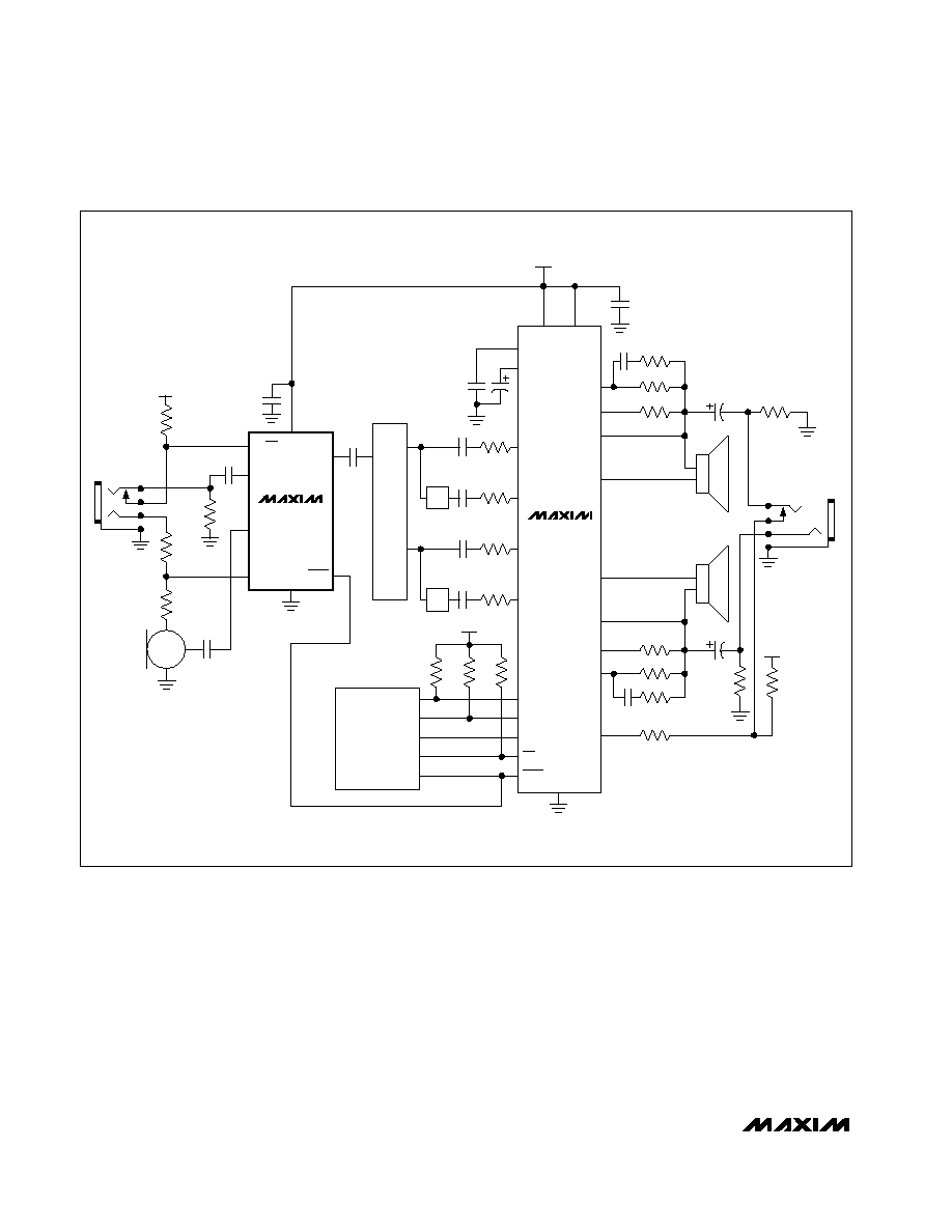
Typical Application Circuit
Figure 1 shows the MAX9813H used as a preamplifier
with the MAX9760 3W audio power amplifier.
PIN
MAX9812L/
MAX9812H
MAX9813L/
MAX9813H
NAME
FUNCTION
1
3
SHDN
Active-Low Shutdown Input. Connect SHDN to V
CC
for normal operation. Connect SHDN
to GND for shutdown. SHDN is a high-impedance input; do not leave floating.
2
2
GND
Ground
3
1
OUT
Amplifier Output
4
8
V
CC
Positive Supply. Bypass V
CC
to GND with a 0.1µF capacitor.
5
7
BIAS
Low-Noise Microphone Bias Output. 2.3V output for MAX9812L/MAX9813L. 4V output for
MAX9812H/MAX9813H.
6
--
IN
Amplifier Input (MAX9812)
--
6
IN1
Amplifer Input 1 (MAX9813)
--
5
IN2
Amplifier Input 2 (MAX9813)
--
4
IN1/IN2
Input Selector. When IN1/IN2 is high, IN1 is selected. When IN1/IN2 low, IN2 is selected.
MAX9812/MAX9813
Tiny, Low-Cost, Single/Dual-Input, Fixed-Gain
Microphone Amplifiers with Integrated Bias
8
_______________________________________________________________________________________
Figure 1. Typical Application Circuit
HPF
HPF
MICROCONTROLLER
CODEC
MAX9813
IN1
IN2
BIAS
OUT
MAX9760
INR2
INR1
INL2
INL1
SV
DD
BIAS
1
µF
0.1
µF
0.68
µF
0.68
µF
0.68
µF
0.68
µF
0.047
µF
0.047
µF
220
µF
220
µF
27.4k
27.4k
47k
10k
10k
680k
33.2k
33.2k
15k
15k
15k
15k
15k
10k
1k
1k
15k
SCL
SDA
ADD
INT
SHDN
GAINLB
GAINLA
OUTL+
OUTL-
OUTR+
GAINRA
GAINRB
OUTR-
HPS
V
DD
V
DD
V
DD
PV
DD
V
DD
V
CC
V
DD
GND
IN1/IN2
2.2k
0.1
µF
0.1
µF
SHDN
0.1
µF
0.1
µF
22k
2.2k
220k
MAX9812/MAX9813
Tiny, Low-Cost, Single/Dual-Input, Fixed-Gain
Microphone Amplifiers with Integrated Bias
_______________________________________________________________________________________
9
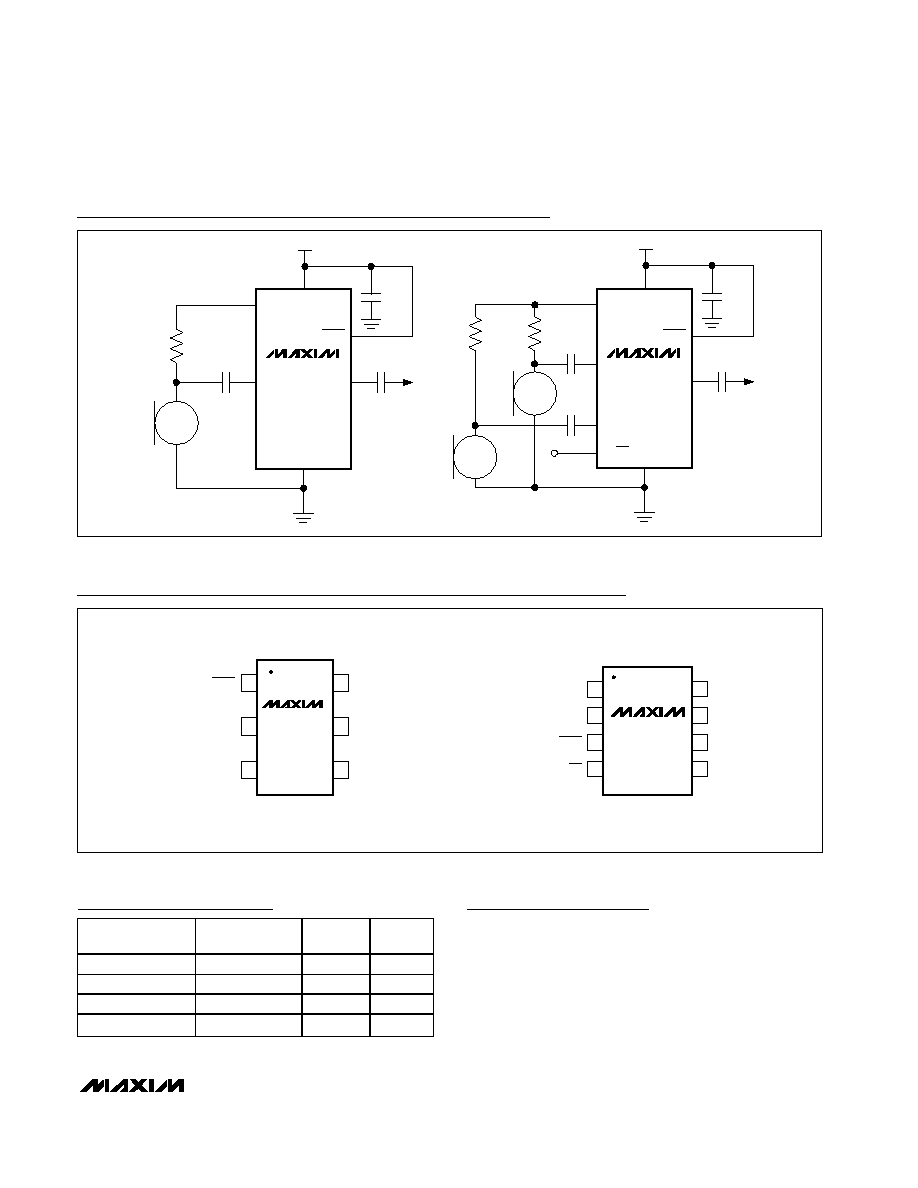
MAX9812
BIAS
IN
SHDN
V
CC
GND
2.2k
0.1
µF
MIC
OUT
V
CC
0.1
µF
0.1
µF
5
6
2
4
3
1
V
BIAS
MAX9813
BIAS
IN1/IN2
IN1
IN2
SHDN
V
CC
GND
2.2k
2.2k
0.1
µF
0.1
µF
MIC1
MIC2
OUT
V
CC
0.1
µF
0.1
µF
7
6
5
4
2
8
1
3
V
BIAS
Chip Information
MAX9812 TRANSISTOR COUNT: 264
MAX9813 TRANSISTOR COUNT: 269
PROCESS: BiCMOS
Typical Operating Circuits
Selector Guide
PART
PIN-PACKAGE
V
CC
(V)
TOP
MARK
MAX9812LEXT-T
6 SC70-6
2.7 to 3.6
ABJ
MAX9812HEXT-T
6 SC70-6
4.5 to 5.5
ABK
MAX9813LEKA-T
8 SOT23-8
2.7 to 3.6
AEEU
MAX9813HEKA-T
8 SOT23-8
4.5 to 5.5
AEEV
SC70
TOP VIEW
GND
V
CC
OUT
1
6
IN
5
BIAS
SHDN
MAX9812
2
3
4
SOT23
IN1
IN2
IN1/IN2
1
2
8
7
V
CC
BIAS
GND
SHDN
OUT
3
4
6
5
MAX9813
Pin Configurations

MAX9812/MAX9813
Tiny, Low-Cost, Single/Dual-Input, Fixed-Gain
Microphone Amplifiers with Integrated Bias
10
______________________________________________________________________________________
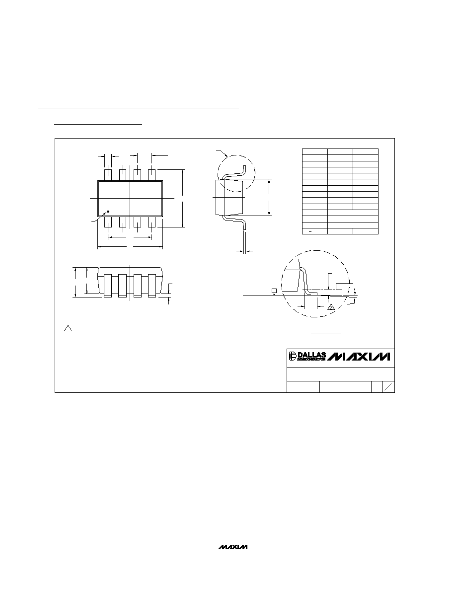
Package Information
(The package drawing(s) in this data sheet may not reflect the most current specifications. For the latest package outline information
go to
www.maxim-ic.com/packages
.)
SC70, 6L.EPS
MAX9812/MAX9813
Tiny, Low-Cost, Single/Dual-Input, Fixed-Gain
Microphone Amplifiers with Integrated Bias
Maxim cannot assume responsibility for use of any circuitry other than circuitry entirely embodied in a Maxim product. No circuit patent licenses are
implied. Maxim reserves the right to change the circuitry and specifications without notice at any time.
Maxim Integrated Products, 120 San Gabriel Drive, Sunnyvale, CA 94086 408-737-7600 ____________________ 11
© 2003 Maxim Integrated Products
Printed USA
is a registered trademark of Maxim Integrated Products.
Package Information (continued)
(The package drawing(s) in this data sheet may not reflect the most current specifications. For the latest package outline information
go to
www.maxim-ic.com/packages
.)
SOT23, 8L .EPS
REV.
DOCUMENT CONTROL NO.
APPROVAL
PROPRIETARY INFORMATION
TITLE:
3.00
2.60
E
C
E1
E
BETWEEN 0.08mm AND 0.15mm FROM LEAD TIP.
8. MEETS JEDEC MO178.
8
0.60
1.75
0.30
L2
0
e1
e
L
1.50
E1
0.65 BSC.
1.95 REF.
0.25 BSC.
GAUGE PLANE
SEATING PLANE C
C
L
PIN 1
I.D. DOT
(SEE NOTE 6)
L
C
L
C
A2
e1
D
DETAIL "A"
5. COPLANARITY 4 MILS. MAX.
NOTE:
7. SOLDER THICKNESS MEASURED AT FLAT SECTION OF LEAD
6. PIN 1 I.D. DOT IS 0.3 MM MIN. LOCATED ABOVE PIN 1.
4. PACKAGE OUTLINE INCLUSIVE OF SOLDER PLATING.
3. PACKAGE OUTLINE EXCLUSIVE OF MOLD FLASH & METAL BURR.
HEEL OF THE LEAD PARALLEL TO SEATING PLANE C.
2. FOOT LENGTH MEASURED FROM LEAD TIP TO UPPER RADIUS OF
1. ALL DIMENSIONS ARE IN MILLIMETERS.
L2
L
A1
A
0.45
1.30
0.15
1.45
MAX
0.28
b
0.90
A2
0.00
A1
0.90
A
MIN
SYMBOL
3.00
0.20
2.80
D
0.09
C
SEE DETAIL "A"
L
C
b
e
D
1
21-0078
1
PACKAGE OUTLINE, SOT-23, 8L BODY
0
0