
1517
Doc #01007
DATA DELAY DEVICES, INC.
1
10/30/01
3 Mt. Prospect Ave. Clifton, NJ 07013
5-TAP DIP DELAY LINE
T
D
/T
R
= 3
(SERIES 1517)
FEATURES
PACKAGES
∑
5 taps of equal delay increment
∑
Delays as large as 300ns available
∑
Low DC resistance
∑
Standard 14-pin DIP package
∑
Epoxy encapsulated
∑
Meets or exceeds MIL-D-23859C
FUNCTIONAL DESCRIPTION
The 1517-series device is a fixed, single-input, five-output, passive delay
line. The signal input (IN) is reproduced at the outputs (T1-T5) in equal
increments. The delay from IN to T5 (T
D
) is given by the device dash
number. The characteristic impedance of the line is given by the letter
code that follows the dash number (See Table). The rise time (T
R
) of the
line is 33% of T
D
, and the 3dB bandwidth is given by 1.05 / T
D
.
SERIES SPECIFICATIONS
FUNCTIONAL DIAGRAM
∑
Dielectric breakdown:
50 Vdc
∑
Distortion @ output:
10% max.
∑
Operating temperature:
-55
∞
C to +125
∞
C
∑
Storage temperature:
-55
∞
C to +125
∞
C
∑
Temperature coefficient: 100 PPM/
∞
C
DASH NUMBER SPECIFICATIONS
Part
Number
Delay
(ns)
Imped
(
)
RDC
(
)
Part
Number
Delay
(ns)
Imped
(
)
RDC
(
)
Part
Number
Delay
(ns)
Imped
(
)
RDC
(
)
1517-10A
10.0
±
1.0
50
0.6
1517-80C
80.0
±
4.0
200
3.5
1517-20F
20.0
±
1.0
400
4.5
1517-15A
15.0
±
1.0
50
0.6
1517-90C
90.0
±
4.5
200
5.0
1517-40F
40.0
±
2.0
400
5.0
1517-20A
20.0
±
1.0
50
0.7
1517-120C
120.0
±
6.0
200
5.0
1517-60F
60.0
±
3.0
400
5.0
1517-30A
30.0
±
1.5
50
0.7
1517-150C
150.0
±
7.5
200
8.0
1517-80F
80.0
±
4.0
400
8.0
1517-40A
40.0
±
2.0
50
0.9
1517-25D
25.0
±
1.3
250
2.5
1517-100F
100.0
±
5.0
400
9.0
1517-5B
5.0
±
1.0
100
0.5
1517-37D
37.0
±
1.9
250
3.0
1517-120F
120.0
±
6.0
400
10.0
1517-10B
10.0
±
1.0
100
0.7
1517-50D
50.0
±
2.5
250
3.5
1517-160F
160.0
±
8.0
400
13.0
1517-15B
15.0
±
1.0
100
0.7
1517-60D
60.0
±
3.0
250
4.0
1517-180F
180.0
±
9.0
400
14.0
1517-20B
20.0
±
1.0
100
0.9
1517-75D
75.0
±
3.8
250
4.0
1517-240F
240.0
±
12.0
400
19.0
1517-25B
25.0
±
1.3
100
1.0
1517-100D
100.0
±
5.0
250
5.0
1517-300F
300.0
±
15.0
400
23.0
1517-30B
30.0
±
1.5
100
1.5
1517-150D
150.0
±
7.5
250
8.5
1517-25G
25.0
±
1.3
500
3.0
1517-40B
40.0
±
2.0
100
1.8
1517-15E
15.0
±
1.0
300
2.5
1517-50G
50.0
±
2.5
500
5.0
1517-50B
50.0
±
2.5
100
2.0
1517-30E
30.0
±
1.5
300
3.0
1517-75G
75.0
±
3.8
500
8.0
1517-60B
60.0
±
3.0
100
2.0
1517-50E
50.0
±
2.5
300
4.0
1517-100G
100.0
±
5.0
500
15.0
1517-75B
75.0
±
3.8
100
2.5
1517-60E
60.0
±
3.0
300
4.0
1517-125G
125.0
±
6.3
500
9.0
1517-10C
10.0
±
1.0
200
1.5
1517-75E
75.0
±
3.8
300
4.5
1517-150G
150.0
±
7.5
500
13.0
1517-20C
20.0
±
1.0
200
2.0
1517-90E
90.0
±
4.5
300
5.5
1517-200G
200.0
±
10.0
500
21.0
1517-30C
30.0
±
1.5
200
2.5
1517-120E
120.0
±
6.0
300
8.0
1517-225G
225.0
±
11.3
500
23.0
1517-40C
40.0
±
2.0
200
3.0
1517-130E
130.0
±
6.5
300
9.0
1517-300G
300.0
±
15.0
500
29.0
1517-50C
50.0
±
2.5
200
3.0
1517-180E
180.0
±
9.0
300
11.0
1517-60C
60.0
±
3.0
200
3.5
1517-220E
220.0
±
11.0
300
13.0
©
©
2001 Data Delay Devices
data
delay
devices,
inc.
Æ
Æ
3
14
13
12
11
10
9
8
1
2
3
4
5
6
7
IN
N/C
T2
N/C
T4
T5
GND
N/C
T1
N/C
T3
N/C
N/C
N/C
1517-xxz
xx = Delay (T
D
)
z = Impedance Code
PIN DESCRIPTIONS
IN
Signal Input
T1-T5 Tap Outputs
GND
Ground
GND
IN
T5
T1
T2
T3
T4
1517
Doc #01007
DATA DELAY DEVICES, INC.
2
10/30/01
Tel: 973-773-2299 Fax: 973-773-9672 http://www.datadelay.com
.780 MAX.
1
2
3
4
5
6
7
8
14
13
12
11
10
9
See
Table
.015 TYP.
.070 MAX.
.018
TYP.
.600
±
.010
6 Equal spaces
each .100
±
.010
Non-Accumulative
.280
MAX.
.350
MAX.
.010
±
.002
Lead Material:
Nickel-Iron alloy 42
TIN PLATE
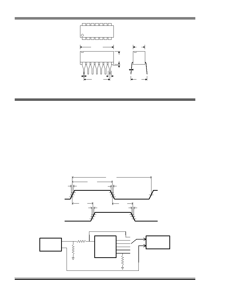
Package Dimensions
PASSIVE DELAY LINE TEST SPECIFICATIONS
TEST CONDITIONS
INPUT:
OUTPUT:
Ambient Temperature:
25
o
C
±
3
o
C
R
load
:
10M
Input Pulse:
High = 3.0V typical
C
load
:
10pf
Low = 0.0V typical
Threshold:
50% (Rising & Falling)
Source Impedance:
50
Max.
Rise/Fall Time:
3.0 ns Max. (measured
at 10% and 90% levels)
Pulse Width
(T
D
<= 75ns):
PW
IN
= 100ns
Period
(T
D
<= 75ns):
PER
IN
= 1000ns
Pulse Width
(T
D
> 75ns):
PW
IN
= 2 x T
D
Period
(T
D
> 75ns):
PER
IN
= 10 x T
D
NOTE: The above conditions are for test only and do not in any way restrict the operation of the device.
Timing Diagram For Testing
D
RISE
D
FALL
PER
IN
PW
IN
T
RISE
T
FALL
10%
10%
50%
50%
90%
90%
50%
50%
V
IH
V
IL
V
OH
V
OL
INPUT
SIGNAL
OUTPUT
SIGNAL
T
RISE
T
FALL
10%
10%
90%
90%
IN
T1
OUT
TRIG
IN
TRIG
Test Setup
DEVICE UNDER
TEST (DUT)
OSCILLOSCOP
PULSE
GENERATOR
50
R
OUT
R
IN
R
IN
= R
OUT
= Z
LINE
T2
T3
T4
T5