1518
Doc #97030
DATA DELAY DEVICES, INC.
1
2/7/97
3 Mt. Prospect Ave. Clifton, NJ 07013
5-TAP SMD DELAY LINE
T
D
/T
R
= 3
(SERIES 1518)
FEATURES
PACKAGES
∑
5 taps of equal delay increment
∑
Delays to 200ns
∑
Low profile
∑
Epoxy encapsulated
∑
Meets or exceeds MIL-D-23859C
FUNCTIONAL DESCRIPTION
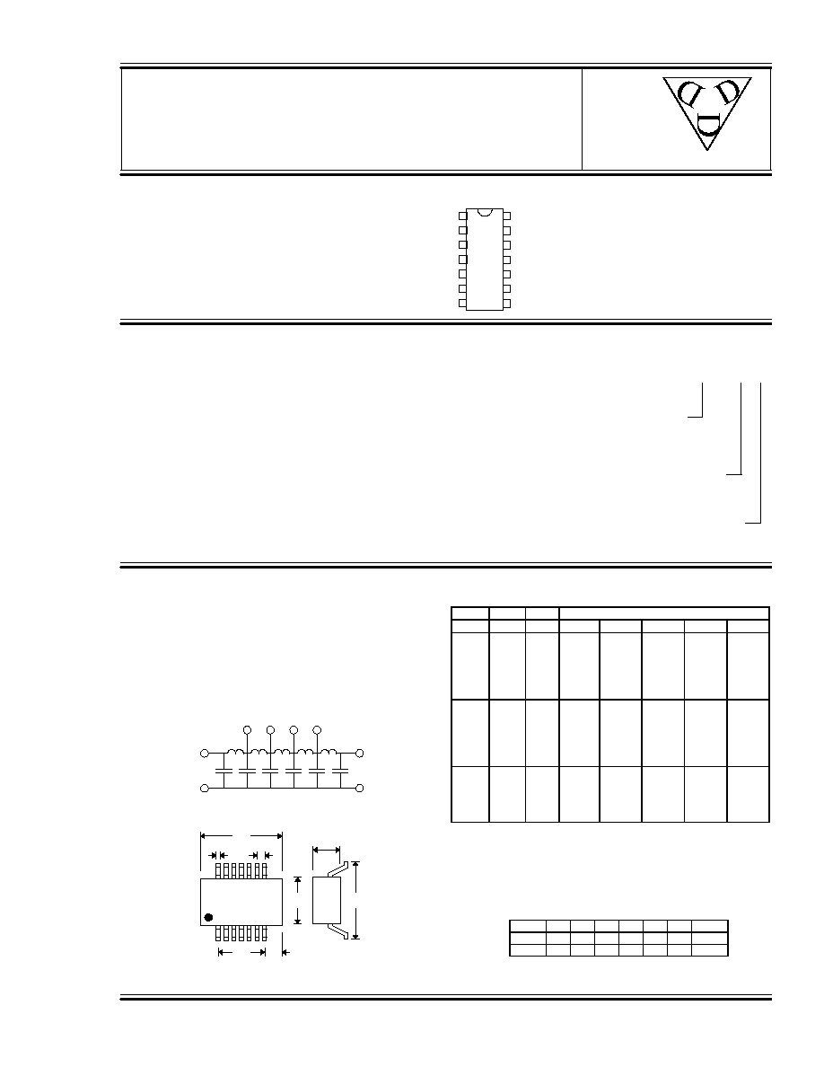
The 1518-series device is a fixed, single-input, five-
output, passive delay line. The signal input (IN) is
reproduced at the outputs (T1-T5) in equal increments.
The delay from IN to T5 (T
D
) and the characteristic
impedance of the line (Z) are determined by the dash
number. The rise time (T
R
) of the line is 30% of T
D
, and
the 3dB bandwidth is given by 1.05 / T
D
. The device is
available in a 14-pin SMD with two pinout options.
Part numbers are constructed according to the scheme
shown at right. For example, 1518-101-500A is a 100ns,
50
delay line with pinout code A. Similarly, 1518-151-
501 a is 150ns, 500
delay line with standard pinout.
SERIES SPECIFICATIONS
∑
Dielectric breakdown:
50 Vdc
∑
Distortion @ output:
10% max.
∑
Operating temperature:
-55
∞
C to +125
∞
C
∑
Storage temperature:
-55
∞
C to +125
∞
C
∑
Temperature coefficient: 100 PPM/
∞
C
GND
IN
T5
T1
T2
T3
T4
GND
Functional Diagram
Package Dimensions
.290
1
7
8
14
.300
.100
.505
.018
.050
.425
.185
data
delay
devices,
inc.
Æ
Æ
3
14
13
12
11
10
9
8
1
2
3
4
5
6
7
IN
N/C
T2
N/C
T4
T5
GND
N/C
T1
N/C
T3
N/C
N/C
N/C
IN
Signal Input
T1-T5 Tap Outputs
GND
Ground
Note: Standard pinout shown
Alt. pinout available
DELAY TIME
Expressed in nanoseconds (ns)
First two digits are significant figures
Last digit specifies # of zeros to follow
IMPEDANCE
Expressed in nanoseconds (ns)
First two digits are significant figures
Last digit specifies # of zeros to follow
PINOUT CODE
See Table
Omit for STD pinout
PART NUMBER CONSTRUCTION
1518 - xxx - zzz p
DELAY SPECIFICATIONS
T
D
T
I
T
R
ATTENUATION (%) TYPICAL
(ns)
(ns)
(ns)
Z=50
Z=100
Z=200
Z=300
Z=500
5
1.0
3.0
N/A
5
N/A
N/A
N/A
10
2.0
4.0
3
5
5
N/A
N/A
15
3.0
5.0
3
5
5
N/A
N/A
20
4.0
6.0
3
5
5
5
N/A
25
5.0
7.0
3
5
5
5
7
30
6.0
10.0
3
5
5
5
7
40
8.0
13.0
3
5
5
5
7
50
10.0
15.0
3
5
5
7
7
60
12.0
20.0
3
5
6
7
8
75
15.0
25.0
3
5
6
7
8
80
16.0
26.0
4
5
6
7
8
100
20.0
30.0
4
5
6
7
8
110
22.0
32.0
4
5
6
7
8
125
25.0
40.0
4
5
6
7
8
150
30.0
50.0
N/A
5
8
10
10
180
36.0
60.0
N/A
7
8
10
10
200
50.0
70.0
N/A
8
10
12
12
Notes: T
I
represents nominal tap-to-tap delay increment
Tolerance on T
D
=
±
±
5% or
±
±
2ns, whichever is greater
Tolerance on T
I
=
±
±
5% or
±
±
1ns, whichever is greater
"N/A" indicates that delay is not available at this Z
PINOUT CODES
CODE
IN
T1
T2
T3
T4
T5
GND
STD
1
13
3
11
5
6
7
A
1
12
4
10
6
7
8,14
©
©
1997 Data Delay Devices
1518
Doc #97030
DATA DELAY DEVICES, INC.
2
2/7/97
Tel: 973-773-2299 Fax: 973-773-9672 http://www.datadelay.com
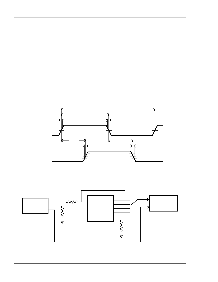
PASSIVE DELAY LINE TEST SPECIFICATIONS
TEST CONDITIONS
INPUT:
OUTPUT:
Ambient Temperature:
25
o
C
±
3
o
C
R
load
:
10M
Input Pulse:
High = 3.0V typical
C
load
:
10pf
Low = 0.0V typical
Threshold: 50% (Rising & Falling)
Source Impedance:
50
Max.
Rise/Fall Time:
3.0 ns Max. (measured
at 10% and 90% levels)
Pulse Width (T
D
<= 75ns): PW
IN
= 100ns
Period
(T
D
<= 75ns): PER
IN
= 1000ns
Pulse Width (T
D
> 75ns): PW
IN
= 2 x T
D
Period
(T
D
> 75ns): PER
IN
= 10 x T
D
NOTE: The above conditions are for test only and do not in any way restrict the operation of the device.
Timing Diagram For Testing
T
RISE
T
FALL
PER
IN
PW
IN
T
RISE
T
FALL
10%
10%
50%
50%
90%
90%
50%
50%
V
IH
V
IL
V
OH
V
OL
INPUT
SIGNAL
OUTPUT
SIGNAL
T
RISE
T
FALL
10%
10%
90%
90%
IN
T1
OUT
TRIG
IN
TRIG
Test Setup
DEVICE UNDER
TEST (DUT)
OSCILLOSCOPE
PULSE
GENERATOR
50
R
OUT
R
IN
R
IN
= R
OUT
= Z
LINE
T2
T3
T4
T5