1520
10-TAP DIP/SMD DELAY LINE
T
D
/T
R
= 5
(SERIES 1520)
FEATURES PACKAGES
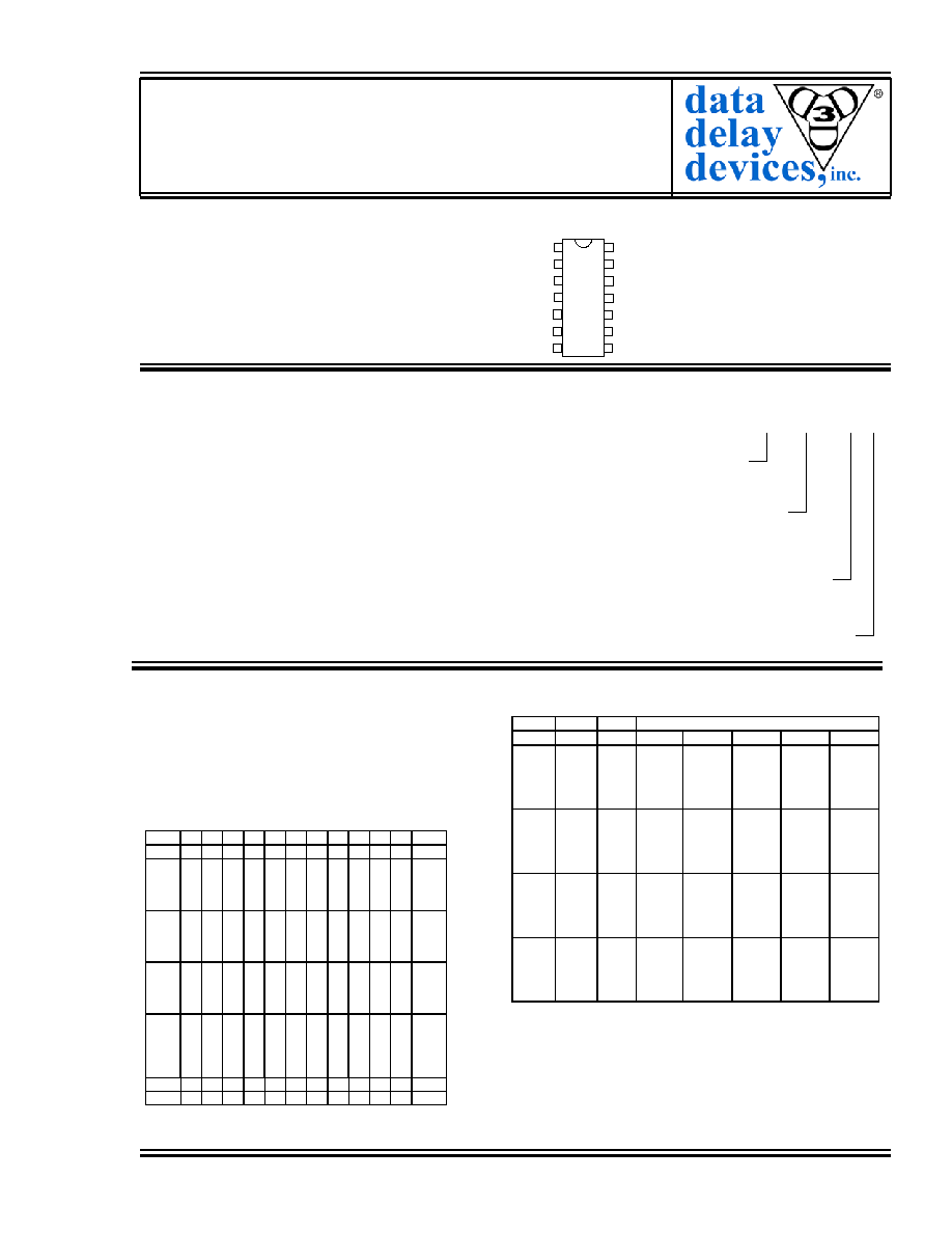
14
13
12
11
10
9
8
1
2
3
4
5
6
7
GND
T1
T3
T5
T6
T8
T10
IN
N/C
T2
T4
T7
T9
GND
� 10 taps of equal delay increment
IN
Signal Input
T1-T10 Tap Outputs
GND
Ground
Note: Standard pinout shown
Other pinouts available
� Delays to 1000ns
� Low profile
� Epoxy encapsulated
� Meets or exceeds MIL-D-23859C
FUNCTIONAL DESCRIPTION
The 1520-series device is a fixed, single-input, ten-output,
passive delay line. The signal input (IN) is reproduced at the
outputs (T1-T10) in equal increments. The delay from IN to T10
(T
D
) and the characteristic impedance of the line (Z) are
determined by the dash number. The rise time (T
R
) of the line is
20% of T
D
, and the 3dB bandwidth is given by 1.75 / T
D
. The
device is available in a 14-pin DIP (1520) or a 14-pin SMD
(1520S), and a wide range of pinouts may be specified.
Part numbers are constructed according to the scheme shown
at right. For example, 1520C-101-500B is a 290 mil DIP,
100ns, 50
delay line with pinout code B. Similarly, 1520SB-
201-251 is a 240 mil SMD, 200ns, 250
delay line with
standard pinout.
DELAY TIME
Expressed in nanoseconds (ns)
First two digits are significant figures
Last digit specifies # of zeros to follow
IMPEDANCE
Expressed in nanoseconds (ns)
First two digits are significant figures
Last digit specifies # of zeros to follow
PINOUT CODE
See Table
Omit for STD pinout
MOUNTING HEIGHT CODE
See Table
PART NUMBER CONSTRUCTION
1520(S)m - xxx - zzz p
SERIES SPECIFICATIONS
DELAY SPECIFICATIONS
T
D
T
I
T
R
ATTENUATION (%) TYPICAL
(ns) (ns) (ns)
Z=50
Z=100 Z=200 Z=300 Z=500
10 1.0 3.0 3
5 N/A N/A N/A
20 2.0 5.5 3
5
5 N/A N/A
30 3.0 6.5 3
5
5 N/A N/A
40
4.0
8.0
3 5 5 5 N/A
50
5.0
10.0
3 5 5 5 7
60
6.0
12.0
3 5 5 5 7
75
7.5
15.0
3 5 5 5 7
100
10.0
20.0
3 5 5 7 7
120
12.0
24.0
3 5 6 7 8
150
15.0
30.0
3 5 6 7 8
180
18.0
36.0
4 5 6 7 8
200
20.0
40.0
4 5 6 7 8
220
22.0
44.0
4 5 6 7 8
250
25.0
50.0
4 5 6 7 8
300 30.0 60.0 N/A
5
8
10
10
375 37.5 75.0 N/A
7
8
10
10
500
50.0
100.0
N/A 8 10 12 12
600 60.0
120.0
N/A N/A N/A 15
15
750 75.0
150.0
N/A N/A N/A 15
20
1000 100.0 200.0
N/A
N/A N/A N/A 20
Notes: T
I
represents nominal tap-to-tap delay increment
Tolerance on T
D
=
�5% or �2ns, whichever is greater
Tolerance on T
I
=
�5% or �1ns, whichever is greater
"N/A" indicates that delay is not available at this Z
�
Dielectric breakdown: 50
Vdc
�
Distortion @ output: 10%
max.
�
Operating temperature: -55
�C to +125�C
�
Storage temperature: -55
�C to +125�C
�
Temperature coefficient: 100
PPM/
�C
PINOUT CODES
CODE IN T1 T2 T3 T4 T5 T6 T7 T8 T9 T10 GND
STD 14 2 12 3 11 4 5 10 6 9 7 1,8
A 1 2 13 3 12 4 10 5 9 6 7 14
B 2 3 4 5 6 7 9 10 11 12 13 1,14
C 7 9 6 10 5 11 12 3 13 2 14
1,8
D 1 13 2 12 3 11 4 10 5 9 6 7,8,14
E 2 3 4 5 6 7,8 9 10 11 12 13 1,14
F 1 13 2 12 3 11 4 10 5 9 6 7
G 2 13 3 12 4 11 5 10 6 9 7 8,14
H 2 3 4 12 6 7 9 10 11 12 13
1
I 1 13 2 12 3 11 5 10 6 9 7 8,14
J 1 2 13 3 12 4 10 5 9 6 7 8,14
K 1 2 3 4 5 6 12 11 10 9 8 7
L 13 12 11 10 9 7,8 6 5 4 3 2 1,14
N 1 2 3 4 5 6 10 11 12 13 14
7
P 1 13 3 12 4 11 5 10 6 9 7 8,14
T 1 2 3 4 5 6 9 10 11 12 13 7,14
U 2 3 4 5 6 8 9 10 11 12 13
1,7
V 2 3 4 5 6 8 9 10 11 12 13
1
W 1 13 2 12 3 11 4 10 5 9 6 7,14
Z 1 13 3 12 4 11 5 10 6 9 8 7
2004 Data Delay Devices
Doc #97028
DATA DELAY DEVICES, INC.
1
5/5/04
3 Mt. Prospect Ave. Clifton, NJ 07013

