3D3215
Doc #01014
DATA DELAY DEVICES, INC.
1
12/3/01
3 Mt. Prospect Ave. Clifton, NJ 07013
MONOLITHIC 5-TAP 3.3V
FIXED DELAY LINE
(SERIES 3D3215)
FEATURES
PACKAGES
∑
All-silicon, low-power 3.3V CMOS technology
∑
Vapor phase, IR and wave solderable
∑
Auto-insertable (DIP pkg.)
∑
Low ground bounce noise
∑
Leading- and trailing-edge accuracy
∑
Delay range: 1.5ns through 300ns
∑
Total delay tolerance: 2% or 0.5ns (3.3V, 25C)
∑
Temperature stability:
±
1% typical (0C-70C)
∑
Vdd stability:
±
1% typical (3.0V-3.6V)
∑
Static Idd: 1.3ma typical
∑
Minimum input pulse width: 25% of total delay
FUNCTIONAL DESCRIPTION
The 3D3215 5-Tap Delay Line product family consists of fixed-delay
3.3V CMOS integrated circuits. Each package contains a single delay
line, tapped and buffered at 5 points spaced uniformly in time. Tap-to-
tap (incremental) delay values can range from 1.5ns through 60ns. The
input is reproduced at the outputs without inversion, shifted in time as
per the user-specified dash number. The 3D3215 is 3.3V CMOS-
compatible and features both rising- and falling-edge accuracy.
The all-CMOS 3D3215 integrated circuit has been designed as a
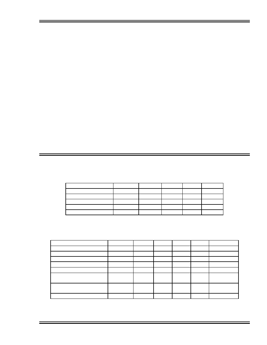
reliable, economic alternative to hybrid fixed delay lines. It is offered in a
standard 8-pin auto-insertable DIP and a space saving surface mount 8-pin SOIC.
TABLE 1: PART NUMBER SPECIFICATIONS
DASH #
DELAY SPECIFICATIONS
INPUT RESTRICTIONS
RECOMMENDED
ABSOLUTE
3D3215Z-xx
3D3215M-xx
TOTAL
DELAY (ns)
TAP-TAP
DELAY (ns)
Max Freq
Min P.W.
Max Freq
Min P.W.
-1.5
6.0
±
0.5*
1.5
±
0.7
23.8 MHz
21.0 ns
83.3 MHz
6.00 ns
-2
8.0
±
0.5*
2.0
±
0.8
20.8 MHz
24.0 ns
83.3 MHz
6.00 ns
-2.5
10.0
±
0.5*
2.5
±
1.0
18.5 MHz
27.0 ns
66.7 MHz
7.50 ns
-3
12.0
±
0.5*
3.0
±
1.3
16.7 MHz
30.0 ns
55.6 MHz
9.00 ns
-4
16.0
±
0.5*
4.0
±
1.3
13.9 MHz
36.0 ns
50.0 MHz
10.00 ns
-5
20.0
±
0.5*
5.0
±
1.4
11.9 MHz
42.0 ns
40.0 MHz
12.50 ns
-6
24.0
±
0.5*
6.0
±
1.4
10.4 MHz
48.0 ns
55.6 MHz
9.00 ns
-8
40.0
±
0.8
8.0
±
1.4
8.33 MHz
60.0 ns
41.7 MHz
12.00 ns
-10
50.0
±
1.0
10.0
±
1.5
6.67 MHz
75.0 ns
40.0 MHz
12.50 ns
-12
60.0
±
1.2
12.0
±
1.5
5.56 MHz
90.0 ns
33.3 MHz
15.00 ns
-15
75.0
±
1.5
15.0
±
1.5
4.42 MHz
113 ns
26.7 MHz
18.75 ns
-20
100
±
2.0
20.0
±
2.0
3.33 MHz
150 ns
20.0 MHz
25.00 ns
-25
125
±
2.5
25.0
±
2.5
2.66 MHz
188 ns
16.0 MHz
31.25 ns
-30
150
±
3.0
30.0
±
3.0
2.22 MHz
225 ns
13.3 MHz
37.50 ns
-40
200
±
4.0
40.0
±
4.0
1.67 MHz
300 ns
10.0 MHz
50.00 ns
-50
250
±
5.0
50.0
±
5.0
1.33 MHz
375 ns
8.0 MHz
62.50 ns
-60
300
±
6.0
60.0
±
6.0
1.11 MHz
450 ns
6.7 MHz
75.00 ns
* Total delay referenced to Tap1 output; Input-to-Tap1 = 7.5ns
±
±
1.5ns
NOTE: Any dash number between 1.5 and 60 not shown is also available as standard
©
©
2001 Data Delay Devices
data
delay
devices,
inc.
Æ
Æ
3
8
7
6
5
1
2
3
4
IN
O2
O4
GND
VDD
O1
O3
O5
3D3215M-xx
DIP (300 Mil)
1
2
3
4
8
7
6
5
IN
O2
O4
GND
VDD
O1
O3
O5
3D3215Z-xx
SOIC (150 Mil)
PIN DESCRIPTIONS
IN
Delay Line Input
O1
Tap 1 Output (20%)
O2
Tap 2 Output (40%)
O3
Tap 3 Output (60%)
O4
Tap 4 Output (80%)
O5
Tap 5 Output (100%)
VDD
+3.3 Volts
GND
Ground
N/C
No Connection
For mechanical dimensions, click
here
.
For package marking details, click
here
.

3D3215
Doc #01014
DATA DELAY DEVICES, INC.
2
12/3/01
Tel: 973-773-2299 Fax: 973-773-9672 http://www.datadelay.com
APPLICATION NOTES
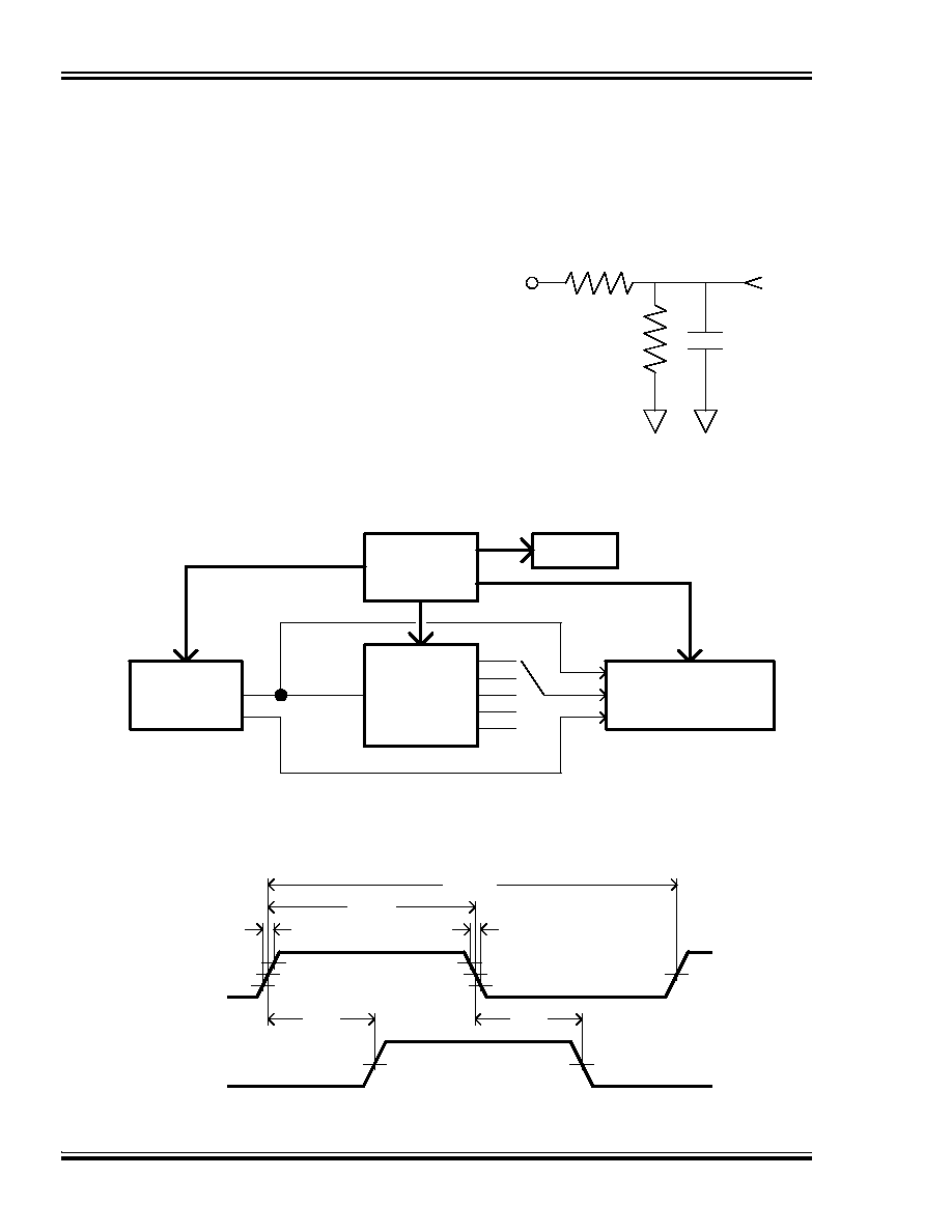
OPERATIONAL DESCRIPTION
The 3D3215 five-tap delay line architecture is
shown in Figure 1. The delay line is composed of
a number of delay cells connected in series.
Each delay cell produces at its output a replica of
the signal present at its input, shifted in time. The
delay cells are matched and share the same
compensation signals, which minimizes tap-to-tap
delay deviations over temperature and supply
voltage variations.
INPUT SIGNAL CHARACTERISTICS
The Frequency and/or Pulse Width (high or low)
of operation may adversely impact the specified
delay accuracy of the particular device. The
reasons for the dependency of the output delay
accuracy on the input signal characteristics are
varied and complex. Therefore a
Recommended
Maximum and an Absolute Maximum operating
input frequency and a
Recommended Minimum
and an
Absolute Minimum operating pulse width
have been specified.
OPERATING FREQUENCY
The
Absolute Maximum Frequency
specification, tabulated in Table 1, determines the
highest frequency of the delay line input signal
that can be reproduced, shifted in time at the
device output, with acceptable duty cycle
distortion.
The
Recommended Maximum Frequency
specification determines the highest frequency of
the delay line input signal for which the output
delay accuracy is guaranteed. To guarantee the
Table 1 delay accuracy for input frequencies
higher than the
Recommended Maximum
Frequency, the 3D3215 must be tested at the
user operating frequency. Therefore, to facilitate
production and device identification, the part
number will include a custom reference
designator identifying the intended frequency of
operation. The programmed delay accuracy of
the device is guaranteed, therefore, only at the
user specified input frequency. Small input
frequency variation about the selected frequency
will only marginally impact the programmed delay
accuracy, if at all.
Nevertheless, it is strongly
recommended that the engineering staff at
DATA DELAY DEVICES be consulted.
OPERATING PULSE WIDTH
The
Absolute Minimum Pulse Width (high or
low) specification, tabulated in Table 1,
determines the smallest Pulse Width of the delay
line input signal that can be reproduced, shifted in
time at the device output, with acceptable pulse
width distortion.
The
Recommended Minimum Pulse Width
(high or low) specification determines the
smallest Pulse Width of the delay line input signal
for which the output delay accuracy tabulated in
Table 1 is guaranteed.
To guarantee the Table 1
delay accuracy for input
pulse width smaller than the Recommended
Minimum Pulse Width, the 3D3215 must be
tested at the user operating pulse width.
Therefore, to facilitate production and device
VDD
O1
IN
O2
O3
O4
Temp & VDD
Compensation
GND
Figure 1: 3D3215 Functional Diagram
25%
25%
25%
25%
O5
VDD
O1
IN
O2
O3
O4
Temp & VDD
Compensation
GND
20%
20%
20%
20%
20%
O5
Dash numbers < 8
Dash numbers >= 8
3D3215
Doc #01014
DATA DELAY DEVICES, INC.
3
12/3/01
3 Mt. Prospect Ave. Clifton, NJ 07013
APPLICATION NOTES (CONT'D)
identification, the part number will include a
custom reference designator identifying the
intended frequency and duty cycle of operation.
The programmed delay accuracy of the device is
guaranteed, therefore, only for the user specified
input characteristics. Small input pulse width
variation about the selected pulse width will only
marginally impact the programmed delay
accuracy, if at all.
Nevertheless, it is strongly
recommended that the engineering staff at
DATA DELAY DEVICES be consulted.
POWER SUPPLY AND
TEMPERATURE CONSIDERATIONS
The delay of CMOS integrated circuits is strongly
dependent on power supply and temperature.
The monolithic 3D3215 delay line utilizes novel
and innovative compensation circuitry to minimize
the delay variations induced by fluctuations in
power supply and/or temperature.
The thermal coefficient is reduced to 200 PPM/C,
which is equivalent to a variation, over the 0C-
70C operating range, of
±
1% or 0.25ns
(whichever is greater) from the 25C delay
settings. The power supply coefficient is reduced,
over the 3.0V-3.6V operating range, to
±
1% or
1ns (whichever is greater) of the delay settings at
the nominal 3.3VDC power supply.
The temperature and power supply sensitivities
are based on the measured delay of Tap 5 with
respect to Tap 1. The sensitivity of the Input-to-
Tap 1 delay will be somewhat higher, particularly
with the smaller dash numbers.
It is essential that the power supply pin be
adequately bypassed and filtered. In addition,
the power bus should be of as low an
impedance construction as possible. Power
planes are preferred.
DEVICE SPECIFICATIONS
TABLE 2: ABSOLUTE MAXIMUM RATINGS
PARAMETER
SYMBOL
MIN
MAX
UNITS
NOTES
DC Supply Voltage
V
DD
-0.3
7.0
V
Input Pin Voltage
V
IN
-0.3
V
DD
+0.3
V
Input Pin Current
I
IN
-1.0
1.0
mA
25C
Storage Temperature
T
STRG
-55
150
C
Lead Temperature
T
LEAD
300
C
10 sec
TABLE 3: DC ELECTRICAL CHARACTERISTICS
(0C to 70C, 3.0V to 3.6V)
PARAMETER
SYMBOL
MIN
TYP
MAX
UNITS
NOTES
Static Supply Current*
I
DD
1.3
2.0
mA
V
DD
= 3.6V
High Level Input Voltage
V
IH
2.0
V
Low Level Input Voltage
V
IL
0.8
V
High Level Input Current
I
IH
-0.1
0.0
0.1
µ
A
V
IH
= V
DD
Low Level Input Current
I
IL
-0.1
0.0
0.1
µ
A
V
IL
= 0V
High Level Output Current
I
OH
-8.0
-6.0
mA
V
DD
= 3.0V
V
OH
= 2.4V
Low Level Output Current
I
OL
6.0
7.5
mA
V
DD
= 3.0V
V
OL
= 0.4V
Output Rise & Fall Time
T
R
& T
F
2
ns
C
LD
= 5 pf
*I
DD
(Dynamic) = 5 * C
LD
* V
DD
* F
Input Capacitance = 10 pf typical
where:
C
LD
= Average capacitance load/tap (pf)
Output Load Capacitance (C
LD
) = 25 pf max
F = Input frequency (GHz)
3D3215
Doc #01014
DATA DELAY DEVICES, INC.
4
12/3/01
Tel: 973-773-2299 Fax: 973-773-9672 http://www.datadelay.com
SILICON DELAY LINE AUTOMATED TESTING
TEST CONDITIONS
INPUT:
OUTPUT:
Ambient Temperature: 25
o
C
±
3
o
C
R
load
:
10K
±
10%
Supply Voltage (Vcc): 3.3V
±
0.1V
C
load
:
5pf
±
10%
Input Pulse:
High = 3.3V
±
0.1V
Threshold: 1.5V (Rising & Falling)
Low = 0.0V
±
0.1V
Source Impedance:
50
Max.
Rise/Fall Time:
3.0 ns Max. (measured
between 0.6V and 2.4V )
Pulse Width:
PW
IN
= 1.5 x Total Delay
Period:
PER
IN
= 3.0 x Total Delay
NOTE: The above conditions are for test only and do not in any way restrict the operation of the device.
10K
470
5pf
Device
Under
Test
Digital
Scope
OUT1
OUT2
OUT4
OUT3
OUT
TRIG
IN
REF
TRIG
Figure 2: Test Setup
DEVICE UNDER
TEST (DUT)
DIGITAL SCOPE/
TIME INTERVAL COUNTER
PULSE
GENERATOR
COMPUTER
SYSTEM
PRINTER
IN
OUT5
Figure 3: Timing Diagram
t
PLH
t
PHL
PER
IN
PW
IN
t
RISE
t
FALL
0.6V
0.6V
1.5V
1.5V
2.4V
2.4V
1.5V
1.5V
V
IH
V
IL
V
OH
V
OL
INPUT
SIGNAL
OUTPUT
SIGNAL