 | ÐлекÑÑоннÑй компоненÑ: PDU13F-.5 | СкаÑаÑÑ:  PDF PDF  ZIP ZIP |
Äîêóìåíòàöèÿ è îïèñàíèÿ www.docs.chipfind.ru
PDU13F
3-BIT PROGRAMMABLE
DELAY LINE
(SERIES PDU13F)
data
delay
devices,
inc.
3
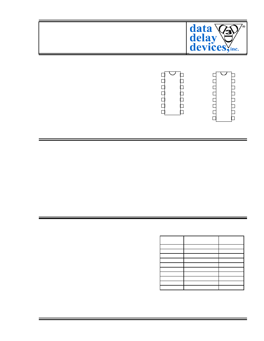
FEATURES PACKAGES
· Digitally programmable in 8 delay steps
14
13
12
11
10
9
8
1
2
3
4
5
6
7
IN
N/C
N/C
OUT
OUT/
EN/
GND
VCC
N/C
N/C
N/C
A0
A1
A2
PDU13F-xx
DIP
PDU13F-xxA2 Gull-Wing
PDU13F-xxB2 J-Lead
PDU13F-xxM Military DIP
PDU13F-xxMC3
Military Gull-Wing
16
15
14
13
12
11
10
9
1
2
3
4
5
6
7
8
IN
N/C
N/C
N/C
OUT
OUT/
EN/
GND
VCC
N/C
N/C
N/C
A0
A1
A2
N/C
· Monotonic delay-versus-address variation
· Two separate outputs: inverting & non-inverting
· Precise and stable delays
· Input & outputs fully TTL interfaced & buffered
· 10 T
2
L fan-out capability
· Fits standard 14-pin DIP socket
· Auto-insertable
FUNCTIONAL DESCRIPTION
The PDU13F-series device is a 3-bit digitally programmable delay line.
The delay, TD
A
, from the input pin (IN) to the output pins (OUT, OUT/)
depends on the address code (A2-A0) according to the following formula:
TD
A
= TD
0
+ T
INC
* A
where A is the address code, T
INC
is the incremental delay of the device,
and TD
0
is the inherent delay of the device. The incremental delay is
specified by the dash number of the device and can range from 0.5ns
through 50ns, inclusively. The enable pin (EN/) is held LOW during
normal operation. When this signal is brought HIGH, OUT and OUT/ are forced into LOW and HIGH
states, respectively. The address is not latched and must remain asserted during normal operation.
PIN DESCRIPTIONS
IN
Delay Line Input
OUT Non-inverted
Output
OUT/ Inverted Output
A2
Address Bit 2
A1
Address Bit 1
A0
Address Bit 0
EN/ Output
Enable
VCC +5
Volts
GND Ground
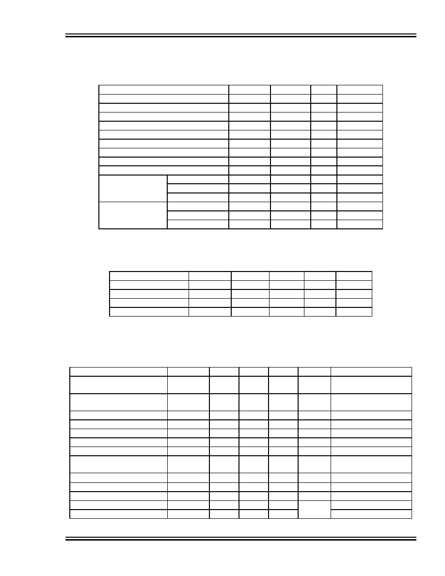
SERIES SPECIFICATIONS
DASH NUMBER SPECIFICATIONS
Part
Number
Incremental Delay
Per Step (ns)
Total Delay
Change (ns)
PDU13F-.5
.5
± .3
3.5
± 1.0
PDU13F-1
1
± .4
7
± 1.0
PDU13F-2
2
± .4
14
± 1.0
PDU13F-3
3
± .5
21
± 1.1
PDU13F-5
5
± .6
35
± 1.8
PDU13F-10
10
± 1.0
70
± 3.5
PDU13F-15
15
± 1.3
105
± 5.3
PDU13F-20
20
± 1.5
140
± 7.0
PDU13F-40
40
± 2.0
280
± 14.0
PDU13F-50
50
± 2.5
350
± 17.5
NOTE: Any dash number between .5 and 50 not
shown is also available.
· Total programmed delay tolerance: 5% or 1ns,
whichever is greater
· Inherent delay (TD
0
): 6ns typical (OUT)
5.5ns typical (OUT/)
· Setup time and propagation delay:
Address to input setup (T
AIS
): 6ns
Disable to output delay (T
DISO
): 6ns typ. (OUT)
· Operating temperature: 0° to 70° C
· Temperature coefficient: 100PPM/°C (excludes TD
0
)
· Supply voltage V
CC
: 5VDC
± 5%
· Supply current: I
CCH
= 45ma
I
CCL
= 20ma
· Minimum pulse width: 20% of total delay
2004 Data Delay Devices
Doc #97001
DATA DELAY DEVICES, INC.
1
3/25/04
3 Mt. Prospect Ave. Clifton, NJ 07013
PDU13F
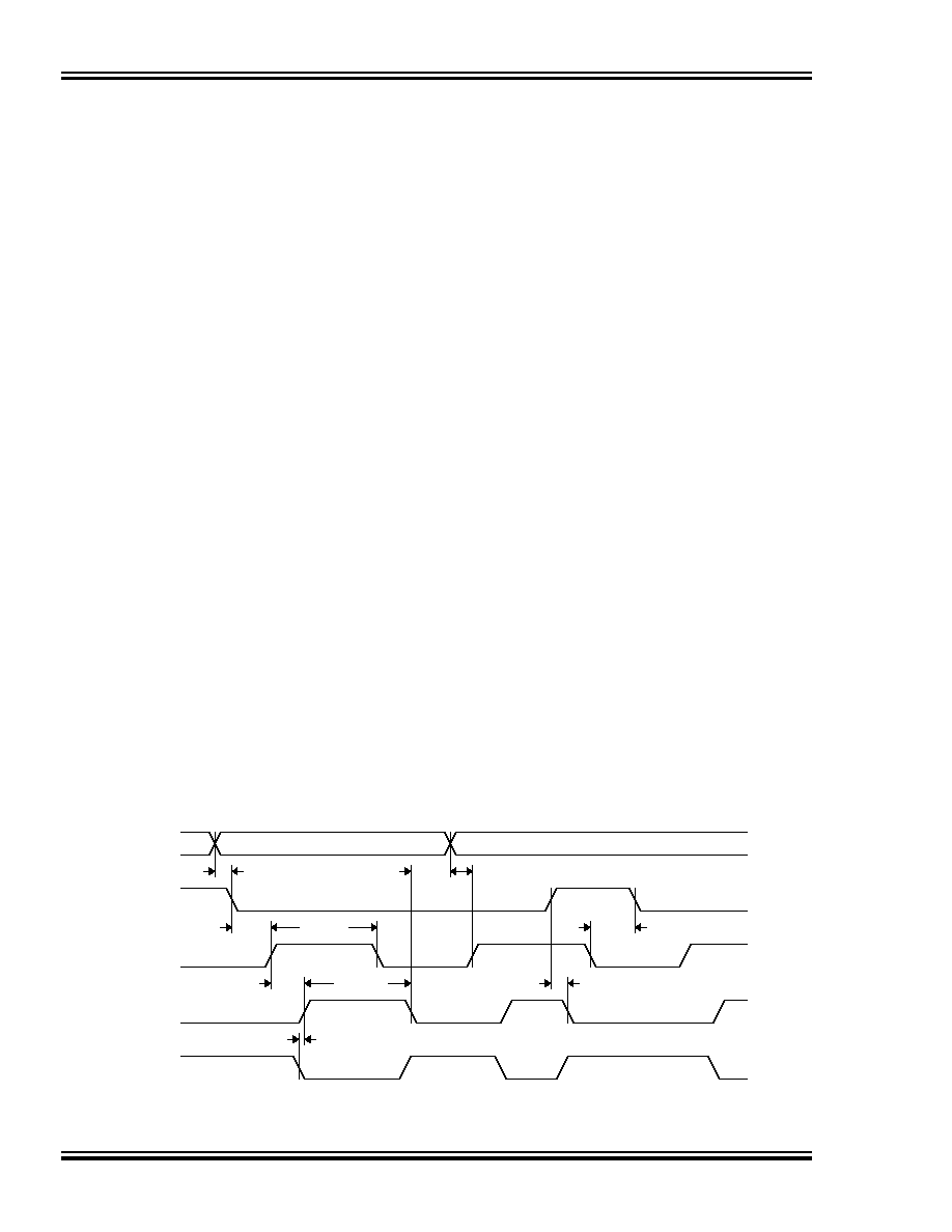
APPLICATION NOTES
ADDRESS UPDATE
The PDU13F is a memory device. As such,
special precautions must be taken when
changing the delay address in order to prevent
spurious output signals. The timing restrictions
are shown in Figure 1.
After the last signal edge to be delayed has
appeared on the OUT pin, a minimum time, T
OAX
,
is required before the address lines can change.
This time is given by the following relation:
T
OAX
= max { (A
i
- A
i-1
) * T
INC
, 0 }
where A
i-1
and A
i
are the old and new address
codes, respectively. Violation of this constraint
may, depending on the history of the input signal,
cause spurious signals to appear on the OUT
pin. The possibility of spurious signals persists
until the required T
OAX
has elapsed.
A similar situation occurs when using the EN/
signal to disable the output while IN is active. In
this case, the unit must be held in the disabled
state until the device is able to "clear" itself. This
is achieved by holding the EN/ signal high and
the IN signal low for a time given by:
T
DISH
= A
i
* T
INC
Violation of this constraint may, depending on the
history of the input signal, cause spurious signals
to appear on the OUT pin. The possibility of
spurious signals persists until the required T
DISH
has elapsed.
INPUT RESTRICTIONS
There are three types of restrictions on input
pulse width and period listed in the AC
Characteristics table. The recommended
conditions are those for which the delay
tolerance specifications and monotonicity are
guaranteed. The suggested conditions are
those for which signals will propagate through the
unit without significant distortion. The absolute
conditions are those for which the unit will
produce some type of output for a given input.
When operating the unit between the
recommended and absolute conditions, the
delays may deviate from their values at low
frequency. However, these deviations will
remain constant from pulse to pulse if the input
pulse width and period remain fixed. In other
words, the delay of the unit exhibits frequency
and pulse width dependence when operated
beyond the recommended conditions. Please
consult the technical staff at Data Delay Devices
if your application has specific high-frequency
requirements.
Please note that the increment tolerances listed
represent a design goal. Although most delay
increments will fall within tolerance, they are not
guaranteed throughout the address range of the
unit. Monotonicity is, however, guaranteed over
all addresses.
T
DISO
T
OAX
T
AENS
T
ENIS
PW
IN
TD
A
PW
OUT
T
DISH
A2-A0
EN/
IN
OUT
OUT/
Figure 1: Timing Diagram
A
i-1
A
i
T
SKEW
T
AIS
Doc #97001
DATA DELAY DEVICES, INC.
2
3/25/04
Tel: 973-773-2299 Fax: 973-773-9672 http://www.datadelay.com
PDU13F
Doc #97001
DATA DELAY DEVICES, INC.
3
3/25/04
3 Mt. Prospect Ave. Clifton, NJ 07013
DEVICE SPECIFICATIONS
TABLE 1: AC CHARACTERISTICS
PARAMETER SYMBOL
MIN
TYP
UNITS
Total Programmable Delay
TD
T
7
T
INC
Inherent Delay
TD
0
6.0
ns
Output Skew
T
SKEW
1.5
ns
Disable to Output Low Delay
T
DISO
6.0
ns
Address to Enable Setup Time
T
AENS
2.0 ns
Address to Input Setup Time
T
AIS
6.0 ns
Enable to Input Setup Time
T
ENIS
6.0 ns
Output to Address Change
T
OAX
See
Text
Disable Hold Time
T
DISH
See
Text
Absolute
PER
IN
20
% of TD
T
Input Period
Suggested
PER
IN
50
% of TD
T
Recommended
PER
IN
200
% of TD
T
Absolute
PW
IN
10
% of TD
T
Input Pulse Width
Suggested
PW
IN
25
% of TD
T
Recommended
PW
IN
100
% of TD
T
TABLE 2: ABSOLUTE MAXIMUM RATINGS
PARAMETER SYMBOL
MIN MAX
UNITS
NOTES
DC Supply Voltage
V
CC
-0.3 7.0 V
Input Pin Voltage
V
IN
-0.3
V
DD
+0.3 V
Storage Temperature
T
STRG
-55 150 C
Lead Temperature
T
LEAD
300
C
10
sec
TABLE 3: DC ELECTRICAL CHARACTERISTICS
(0C to 70C, 4.75V to 5.25V)
PARAMETER SYMBOL
MIN
TYP
MAX
UNITS NOTES
High Level Output Voltage
V
OH
2.5
3.4 V
V
CC
= MIN, I
OH
= MAX
V
IH
= MIN, V
IL
= MAX
Low Level Output Voltage
V
OL
0.35
0.5
V
V
CC
= MIN, I
OL
= MAX
V
IH
= MIN, V
IL
= MAX
High Level Output Current
I
OH
-1.0
mA
Low Level Output Current
I
OL
20.0
mA
High Level Input Voltage
V
IH
2.0 V
Low Level Input Voltage
V
IL
0.8
V
Input Clamp Voltage
V
IK
-1.2
V
V
CC
= MIN, I
I
= I
IK
Input Current at Maximum
Input Voltage
I
IHH
0.1
mA
V
CC
= MAX, V
I
= 7.0V
High Level Input Current
I
IH
20
µA
V
CC
= MAX, V
I
= 2.7V
Low Level Input Current
I
IL
-0.6
mA
V
CC
= MAX, V
I
= 0.5V
Short-circuit Output Current
I
OS
-60 -150
mA
V
CC
= MAX
Output High Fan-out
25
Unit
Output Low Fan-out
12.5
Load
PDU13F
Doc #97001
DATA DELAY DEVICES, INC.
4
3/25/04
Tel: 973-773-2299 Fax: 973-773-9672 http://www.datadelay.com
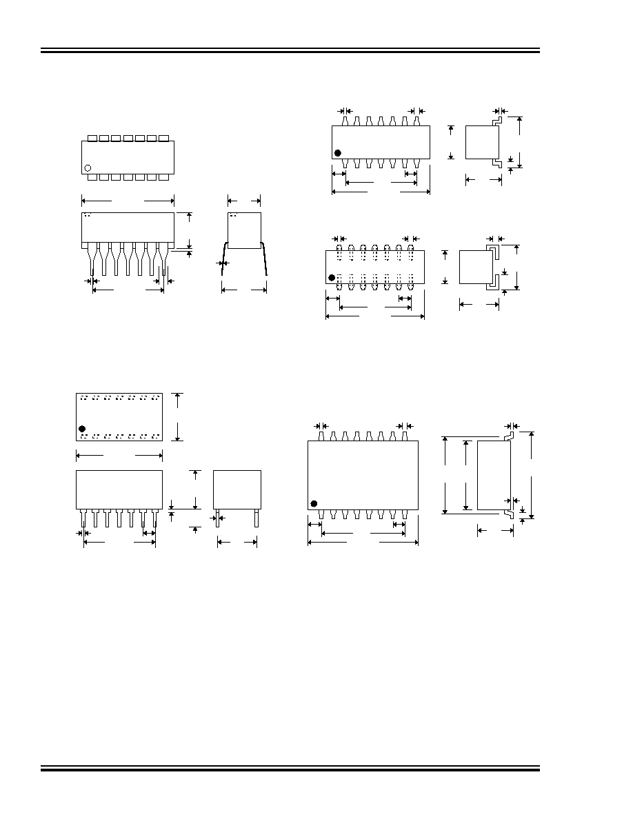
PACKAGE DIMENSIONS
.790 MAX.
.430
TYP.
.020 TYP.
.040
TYP.
.100
.090
.600
.300
MAX.
.270
TYP.
.010 TYP.
.050
TYP.
1
2
3
4
5
6
7
8
9
10
11
12
13
14
Commercial Gull-Wing (PDU13F-xxA2)
.820 MAX.
1
2
3
4
5
6
7
8
14 13 12 11 10
9
.290
MAX.
.015 TYP.
.070 MAX.
.018
TYP.
.600
±.010
6 Equal spaces
each .100
±.010
Non-Accumulative
.280
MAX.
.350
MAX.
.010
±.002
Lead Material:
Nickel-Iron alloy 42
TIN PLATE
Commercial DIP (PDU13F-xx)
.790 MAX.
1
2
3
4
5
6
7
8
.320
TYP.
.020 TYP.
.040
TYP.
.100
.110
.600
.350
MAX.
.270
TYP.
.050 TYP.
.110
TYP.
9
10
11
12
13
14
Commercial J-Lead (PDU13F-xxB2)
.130
±.030
.820 MAX.
1 2
3
4
5
6
7
8
14 13 12 11 10
9
.320
MAX.
.018 TYP.
.410
TYP.
.300
TYP.
.020 TYP.
.600 TYP.
.020
TYP.
.100
TYP.
Military DIP (PDU13F-xxM)
.880
±.020
.882
±.005
.020 TYP.
.040
TYP.
.100
.090
.700
.280
MAX.
.590
MAX.
.010
±.002
.050
±.010
.710
±.005
.007
±.005
1
2
3
4
5
6
7
8
9
10
11
12
13
14
15
16
Military Gull-Wing (PDU13F-xxMC3)
PDU13F
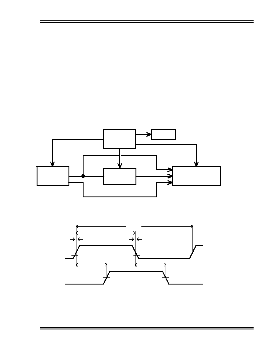
DELAY LINE AUTOMATED TESTING
TEST CONDITIONS
INPUT:
OUTPUT:
Ambient Temperature: 25
o
C
± 3
o
C
Load:
1 FAST-TTL Gate
Supply Voltage (Vcc): 5.0V
± 0.1V
C
load
: 5pf
± 10%
Input Pulse:
High = 3.0V
± 0.1V
Threshold: 1.5V (Rising & Falling)
Low = 0.0V
± 0.1V
Source Impedance: 50
Max.
Rise/Fall Time:
3.0 ns Max. (measured
between 0.6V and 2.4V )
Pulse Width: PW
IN
= 1.5 x Total Delay
Period: PER
IN
= 4.5 x Total Delay
NOTE: The above conditions are for test only and do not in any way restrict the operation of the device.
OUT
OUT
TRIG
IN
REF
TRIG
Test Setup
DEVICE UNDER
TEST (DUT)
TIME INTERVAL
COUNTER
PULSE
GENERATOR
COMPUTER
SYSTEM
PRINTER
IN
Timing Diagram For Testing
TD
AR
TD
AF
PER
IN
PW
IN
T
RISE
T
FALL
0.6V
0.6V
1.5V
1.5V
2.4V
2.4V
1.5V
1.5V
V
IH
V
IL
V
OH
V
OL
INPUT
SIGNAL
OUTPUT
SIGNAL
Doc #97001
DATA DELAY DEVICES, INC.
5
3/25/04
3 Mt. Prospect Ave. Clifton, NJ 07013