DATEL, Inc., Mansfi eld, MA 02048 (USA)
∑
Tel: (508)339-3000, (800)233-2765 Fax: (508)339-6356
∑
E≠mail: sales@datel.com
∑
Internet: www.datel.com
ADC-208A
8-Bit, 20MSPS CMOS Flash A/D
(ADC-208 Compatible)
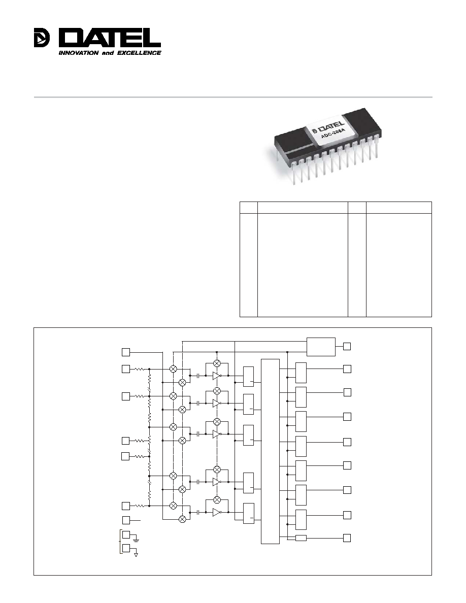
Figure 1. ADC-208A Block Diagram
Æ
Æ
FEATURES
∑
8-bit fl ash A/D converter
∑
20MHz sampling rate
∑
10MHz full-power bandwidth
∑
Sample-hold not required
∑
Low power CMOS
∑
+5Vdc operation
∑
1.2 Micron CMOS
∑
8-Bit latched outputs
∑
Surface-mount version
∑
No missing codes
GENERAL DESCRIPTION
The ADC-208A utilizes an advanced VLSI 1.2 micron CMOS
in providing 20MHz sampling rates at 8-bits. The fl exibility
of the design architecture and process delivers latch-up free
operation without external components and operation over the
full military range.
The ADC-208A is mechanically and electrically equivalent to
the ADC-208 Series, with the exception of the OVERFLOW
(pin 13) and ENABLE (pins 11 and 12) functions. These
functions are not offered on the ADC-208A.
1 VDD 24 BIT 8 (LSB)
2 CLOCK INPUT 23 BIT 7
3 ≠REFERENCE 22 BIT 6
4 ANA/DIG GND (VSS) 21 BIT 5
5 ANALOG INPUT 20 REF 1/4 FS
6 REF MIDPOINT 19 VDD
7 ANALOG INPUT 18 REF 3/4 FS
8 ANA/DIG GND (VSS) 17 BIT 4
9 +REFERENCE 16 BIT 3
10 VDD 15 BIT 2
11 N.C. 14 BIT 1 (MSB)
12 N.C. 13 N.C.
PIN FUNCTION PIN FUNCTION
ANALOG INPUT
R2
1
1
1
R
R
R
R2
R2
R2
R2
+REFERENCE
æ REFERENCE
º REFERENCE
≠ REFERENCE
MIDPOINT
REFERENCE
CLOCK
CLOCK
GENERATOR
BIT 1
BIT 2
BIT 3
BIT 4
BIT 5
BIT 6
BIT 7
BIT 8
(LSB)
256 to
7 ENCODER
5,7
PINS 1, 10, 19 +5V
PINS 4-8
DIGITAL GND
ANALOG GND
+V
DD
9
18
6
20
3
2
14
02
02
01
01
15
16
17
21
22
23
24
D
G
Q
D
G
Q
D
G
Q
D
G
Q
D
G
Q
D
G
Q
D
G
Q
D
G
Q
D
G
Q
D
G
Q
D
G
Q
D
G
Q
INPUT/OUTPUT CONNECTIONS
2
DATEL, Inc., Mansfi eld, MA 02048 (USA)
∑
Tel: (508)339-3000, (800)233-2765 Fax: (508)339-6356
∑
E≠mail: sales@datel.com
∑
Internet: www.datel.com
ADC-208A
Æ
Æ
PERFORMANCE MIN. TYP. MAX. UNITS
Int. Linearity Over Temp.
(ref. unadjusted)
End-point -- ±2.3 ±2.6 LSB
Best-fi t Line -- ±1.8 ±2.0 LSB
Zero-Scale Offset -- ±1 ±2 LSB
(Code "0" to "1" transition)
Gain Error -- ±1.5 ±3 LSB
Differential Gain -- 2 -- %
Differential Phase -- 1.1 -- degrees
Aperture Delay -- 8 -- ns
Aperture Jitter -- 50 -- ps
Harmonic Distortion
(8MHz second order harm.) ≠40 ≠46 -- dB
Ref. bandwidth
(See tech note 5) -- 10 -- MHz
Power Supply Rejection -- ±0.02 ±0.05 %FSR/%Vs
No Missing Codes Over the operating temperature range
POWER REQUIREMENTS
Power Supply Range (+V
DD
) +3.0 +5.0 +5.5 Volts
Power Supply Current
+25∞C -- +45 +65 mA
+125∞C -- +40 +60 mA
≠55∞C -- +50 +70 mA
Power Dissipation
+25∞C -- 225 325 mW
+125∞C -- 200 300 mW
≠55∞C -- 250 350 mW
PHYSICAL ENVIRONMENTAL
Operating Temp. Range, Case:
MC/LM Versions 0 -- +70 ∞C
MM/LM/QL Versions ≠55 -- +125 ∞C
Storage Temp. Range ≠65 -- +150 ∞C
Package Type
DIP 24-pin ceramic DIP
LCC 24-pin ceramic LCC
PARAMETERS LIMITS UNITS
Power Supply Voltage (V
DD
Pin 1, 10, 19) ≠0.5 to +7 Volts
Digital Inputs ≠0.5 to +5.5 Volts
Analog Input ≠0.5 to (+V
DD
+0.5) Volts
Reference Inputs ≠0.5 to (+V
DD
+0.5) Volts
Digital Outputs ≠0.5 to +5.5 Volts
(short circuit protected to ground)
Lead Temperature (10 sec. max.) +300 max. ∞C
Storage Temperature ≠65 to +150 ∞C
FUNCTIONAL SPECIFICATIONS
(Typical at +5V power, +25∞C, 20MHz clock, +REFERENCE = +5V,
≠REFERENCE = ground, unless noted)
ABSOLUTE MAXIMUM RATINGS
ANALOG INPUT MIN. TYP. MAX. UNITS
Single-Ended, Non-Isolated
Input Range DC - 20MHz 0 ≠ +5.0 Volts
Analog Input Capacitance
(static - Pin 5 to 7) ≠ 20 ≠ pF
(dynamic - Pin 5 to 7) ≠ 64 ≠ pF
Reference Ladder Resistance ≠ 500 ≠ Ohms
Reference Input (Note 5) ≠0.5 ≠ V
DD
+0.5 Volts
DIGITAL INPUTS
Logic Levels
Logic "1" 3.2 -- -- Volts
Logic "0" -- -- 0.8 Volts
Logic Loading
Logic Loading "1" -- +1 +5 µA
Logic Loading "0" -- +1 +5 µA
Clock Low Pulse Width 15 25 -- nSec
DIGITAL OUTPUTS
Logic Levels
Logic "1" 2.4 4.5 5.0 Volts
Logic "0" -- -- 0.4 Volts
Logic Loading
Logic Loading "1" 4 -- -- mA
Logic Loading "0" 4 -- -- mA
Output Data Valid Delay From
Rising Clock Edge
99% probability 5 10 15 nSec
100% probability
+25∞C 5 10 25 nSec
≠55∞C to +125∞C -- -- 40 nSec
Data Output Resolution 8 -- -- Bits
Data Coding Straight binary
PERFORMANCE
Sampling Rate
15 20 -- MSPS
Full Power Bandwidth 10 -- -- MHz
Diff. Linearity @ +25∞C
(See tech note 7)
Code Transitions -- ±0.5 ±1.0 LSB
Center of Codes -- ±0.25 -- LSB
Diff. Linearity Over Temp.
Code Transitions -- ±0.5 ±1.0 LSB
Center of Codes -- ±0.25 -- LSB
Int. Linearity @ +25∞C
(See tech note 4)(ref. adjusted)
End-point -- -- ±1/2 LSB
Best-fi t Line -- -- ±1/2 LSB
Int. Linearity Over Temp.
(ref. adjusted)
Best-fi t Line -- ±1/2 ±1 LSB
Int. Linearity @ +25∞C
(ref. unadjusted)
End-point -- ±2 ±2.6 LSB
Best-fi t Line -- ±1.6 ±1.9 LSB
Footnotes:
Maximum input impedance is a function of clock frequency.
At full-power input.
For 10-step, 40 IRE NTSC ramp test.
TECHNICAL NOTES
1. The Reference ladder is fl oating with respect to VDD
and may be referenced anywhere within the specifi ed
limits. AC modulation of the reference voltage may also
be utilized; contact DATEL for further information.
2. Clock Pulse Width ≠ To improve performance when input
signals may exceed Nyquist bandwidths, the clock duty
cycle can be adjusted so that the low portion (sample
mode) of the clock pulse is 15nSec wide. Reducing
the sampling time period minimizes the amount the
input voltage slews and prevents the comparators from
saturating.
3. A full-scale input produces all "1" on the data outputs.
4. DATEL uses the conservative defi nitions when specifying
Intergal Linearity (end-point) and Differential Linearity (code
transition). The specifi cations using the less conservative
defi nition have also been provided as a comparative
specifi cation for products specifi ed this way.
3
DATEL, Inc., Mansfi eld, MA 02048 (USA)
∑
Tel: (508)339-3000, (800)233-2765 Fax: (508)339-6356
∑
E≠mail: sales@datel.com
∑
Internet: www.datel.com
ADC-208A
Æ
Æ
5. The process that is used to fabricate the ADC-208A
eliminates the latchup phenomena that has plagued
CMOS devices in the past. These converters do not
require external protection diodes.
6. For clock rates less than 100kHz, there may be
some degradation in offset and differential nonlinearity.
Performance may be improved by increasing the clock
duty cycle (decreasing the time spent in the sample
mode).
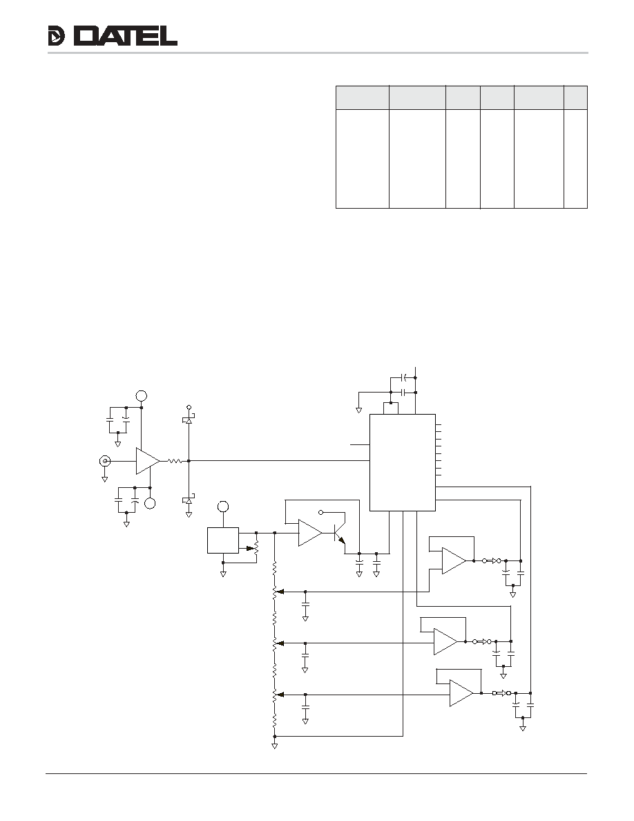
7. Connect the converter appropriately; a typical
connection circuit is shown in Figure 2. Then apply an
appropriate clock input.The reference input should be
held to ±0.1% accuracy or better. Do not use the +5V
power supply as a reference without precision regulation
and high-frequency decoupling capacitors.
8. Zero Adjustment - Adjusting the voltage at
≠REFERENCE (pin 3) adjusts the offset or zero of the
device. Pin 3 can be tied to GROUND for operation
without adjustments
9. Full Scale Adjustment - Adjusting the voltage at
+REFERENCE (pin 9) adjusts the gain of the device. Pin
9 can be tied directly to a +5V reference for operation
without adjustment.
Table 1. ADC-208A Output Code
Note:
Values shown here are for a +5.12Vdc reference. Scale other refereces
proportionally. (+REF=+5.12V, ≠REF=GND, º, Ω, and æ References
FS=No Connection)
10.Integral Nonlinearity Adjustments - Provision is made
for optional adjustment of Integral Nonlinearity through
access of the reference's º, Ω, and æ full scale points.
For example, the REF. MIDPOINT (pin 6) can be tied to
a precision voltage halfway between +REFERENCE and
≠REFERENCE. Pins 6, 18 and 20 should be bypassed
to GROUND through 0.1µF capacitors for operation
without INL adjustments
Figure 2. ADC-208A Typical Connection Diagram
ANALOG DATA DATA
INPUT CODE 1234 5678 DECIMAL HEX
0.00V Zero 0000 0000 0000 0 00
+0.02V +1 LSB 0000 0001 1 01
+1.28V +º FS 0100 0000 64 40
+2.54V +Ω FS-ILSB 0111 1111 127 7F
+2.56V +Ω FS 1000 0000 128 80
+2.58V +Ω FS+ILSB 1000 0001 129 81
+3.84V +æ FS 1100 0000 192 C0
+5.10V +FS 1111 1111 255 FF
REF. D2
20MHz CLOCK
VIN 5,7
Ræ
CLOCK 2
D GND 4
REF-3
REF MID 6
REF+9
A GND 8
VDD 1,10,19
HP2811
+5V
+5V
+15
+15V
+15V
≠15
11
20
18
12
+
+
+
+
+
+
+
5
5
6
4
2
2
9
6
7
5
12
13
14
10
8
1
3
10
0.1µF
0.1µF
0.1µF
0.1µF
0.1µF
0.1µF
0.1µF
0.1µF
10
10k
2k
1k
1k
1k
1.5k
1.5k
2k
0.1µF
0.01µF
4.7µF
4.7µF
4.7µF
4.7µF
4.7µF
4.7µF
4.7µF
HA-5033
LM324
1+N
1-N
LM324
1+N
1-N
LM324
1+N
1-N
LM324
1+N
1-N
24 (LSB)
23
22
21
17
16
15
14 (MSB)
B8
B7
B6
B5
B4
B3
B2
B1
Rº

4
ADC-208A
Æ
Æ
DATEL, Inc. 11 Cabot Boulevard, Mansfi eld, MA 02048-1151
Tel: (508) 339-3000 (800) 233-2765 Fax: (508) 339-6356
Internet: www.datel.com Email: sales@datel.com
DATEL (UK) LTD. Tadley, England Tel: (01256)-880444
DATEL S.A.R.L. Montigny Le Bretonneux, France Tel: 01-34-60-01-01
DATEL GmbH M¸nchen, Germany Tel: 89-544334-0
DATEL KK Tokyo, Japan Tel: 3-3779-1031, Osaka Tel: 6-6354-2025
DATEL makes no representation that the use of its products in the circuits described herein, or the use of other technical information contained herein, will not infringe upon existing or future patent rights. The descriptions contained herein do
not imply the granting of licenses to make, use, or sell equipment constructed in accordance therewith. Specifi cations are subject to change without notice. The DATEL logo is a registered DATEL, Inc. trademark.
DS-0500C 01/03
Æ
Æ
ADC-208A LCC
ADC-208A DIP
0.250 ±0.005
(6.35)
0.050
(1.27)
0.090 Max.
(2.28)
0.400 SQ.
+0.010, ≠0.005
(10.16)
0.020 ±0.005
(0.50)
Pin 1
Pin 9
Pin 21
1.250
(31.7)
PIN 1
IDENTIFIER
0.500
(12.7)
DATEL
ADC-208A
0.020
(0.5)
0.100
(2.5)
0.050
(1.3)
0.610
(15.5)
0.190
(4.9)
0.190
(4.9)
0.38
(9.7)
01
02
01
02
01
02
AUTO ZERO
SAMPLE
N
N DATA
N+1 DATA
AUTO ZERO
SAMPLE
N+1
AUTO ZERO
SAMPLE
N+2
40nSec max.
40nSec max.
MODEL TEMP. RANGE
PACKAGE
ADC-208AMC
0∞C to +70∞C
24-pin DIP
ADC-208AMM
≠55∞C to +125∞C
24-pin DIP
ADC-208ALC
0∞C to +70∞C
24-pin DIP
ADC-208ALM
≠55∞C to +125∞C
24-pin LCC
Figure 3 Timing Diagram
The ADC-208AMM-QL replaces the ADC-208MM-QL and includes DATEL
QL High-Reliability Screening.
The ADC-208ALM-QL replaces the ADC-208LM.
ORDERING INFORMATION
MECHNICAL DIMENSIONS