
Æ
Æ
Figure 1. ADS-117 Functional Block Diagram
DATEL, Inc., 11 Cabot Boulevard, Mansfield, MA 02048-1151 (U.S.A.)
∑
Tel: (508) 339-3000 Fax: (508) 339-6356
∑
For immediate assistance: (800) 233-2765
ADS-117
12-Bit, 2MHz, Low-Power
Sampling A/D Converters
FEATURES
∑
12-bit resolution
∑
No missing codes
∑
2MHz minimum throughput
∑
Functionally complete
∑
Small 24-pin DDIP
∑
Low-power, 1.6 Watts
∑
Three-state output buffers
∑
Samples to Nyquist frequencies
GENERAL DESCRIPTION
DATEL's ADS-117 is a functionally complete, 12-bit, 2MHz,
sampling A/D converter. Its standard, 24-pin, double-width
DIP contains a fast-settling sample-hold amplifier, a 12-bit
subranging (two-step) A/D converter, a precision reference,
three-state output register and all the timing and control logic
necessary to operate from a single start convert pulse. Digital
input and output levels are TTL.
Total harmonic distortion (THD) and signal-to-noise ratio
(including distortion) typically run ≠78dB and 70dB,
respectively, with full scale inputs up to 100kHz. The ADS-117
requires ±15V and +5V power supplies and typically
consumes 1.6 Watts. Models are available for use in either
commercial (0 to +70∞C) or military (≠55 to +125∞C) operating
temperature ranges.
INPUT/OUTPUT CONNECTIONS
PIN
FUNCTION
PIN
FUNCTION
1
BIT 12 (LSB)
24
≠15V SUPPLY
2
BIT 11
23
ANALOG GROUND
3
BIT 10
22
+15V SUPPLY
4
BIT 9
21
+10V REFERENCE
5
BIT 8
20
BIPOLAR
6
BIT 7
19
ANALOG INPUT
7
BIT 6
18
COMP BIN
8
BIT 5
17
ENABLE (1-12)
9
BIT 4
16
START CONVERT
10
BIT 3
15
EOC
11
BIT 2
14
DIGITAL GROUND
12
BIT 1 (MSB)
13
+5V SUPPLY
REF
R
E
G
I
S
T
E
R
R
E
G
I
S
T
E
R
3
-
S
T
A
T
E
O
U
T
P
U
T
R
E
G
I
S
T
E
R
12 BIT 1 (MSB)
11 BIT 2
10 BIT 3
9 BIT 4
8 BIT 5
7 BIT 6
6 BIT 7
5 BIT 8
4 BIT 9
3 BIT 10
2 BIT 11
1 BIT 12 (LSB)
TIMING AND
CONTROL LOGIC
BIPOLAR 20
+10V REF. 21
START CONVERT 16
EOC 15
D
I
G
I
T
A
L
C
O
R
R
E
C
T
I
O
N
L
O
G
I
C
DAC
FLASH
ADC
COMP BIN 18
BUFFER
≠
+
S/H
ANALOG INPUT 19
17 ENABLE (1-12)
S
2
S
1
13
+5V SUPPLY
22
+15V SUPPLY
23
ANALOG GROUND
14
DIGITAL GROUND
24
≠15V SUPPLY

Æ
Æ
ADS-117
2
FUNCTIONAL SPECIFICATIONS
(T
A
= +25∞C, ±V
CC
= +15V, +V
DD
=+5V, 2MHz sampling rate, and a minimum 3 minute
warmup unless otherwise specified.)
ANALOG INPUTS
MIN.
TYP.
MAX.
UNITS
Input Voltage Range
Bipolar
--
±5
--
Volts
Unipolar
--
0 to +10
--
Volts
Input Impedence
4.5
5
--
k
Input Capacitance
--
6
15
pF
DIGITAL INPUTS
Logic Levels
Logic "1"
+2.0
--
--
Volts
Logic "0"
--
--
+0.8
Volts
Logic Loading "1"
--
--
+5
µA
Logic Loading "0"
--
--
≠600
µA
PERFORMANCE
Resolution
12 Bits
No Missing Codes
(12 Bits; f
in
= 1MHz)
0 to +70∞C
Integral Non-Linearity
0∞C to +70∞C
--
±1/2
±2
LSB
≠55∞C to +125∞C
--
±1
±3
LSB
Differential Non-Linearity
0∞C to +70∞C
--
±1/2
±0.95
LSB
≠55∞C to +125∞C
--
±1
+1.5
LSB
Full Scale Absolute Accuracy
(see Tech Note 1)
0∞C to +70∞C
--
±0.13
±0.44
%FSR
≠55∞C to +125∞C
--
±0.25
±0.73
%FSR
Unipolar/Bipolar Zero Error
0∞C to +70∞C (see Tech Note 1)
--
±0.07
±0.27
%FSR
≠55∞C to +125∞C
--
±0.22
±0.73
%FSR
Bipolar Offset Error
0∞C to +70∞C (see Tech Note 1)
--
±0.1
±0.38
%FSR
≠55∞C to +125∞C
--
±0.53
±0.73
%FSR
Gain Error (see Tech Note 1)
0∞C to +70∞C
--
±0.1
±0.38
%
≠55∞C to +125∞C
--
±0.53
±0.73
%
Internal Reference Voltage
0∞C to +70∞C
+9.97
+10.0
+10.03
Volts
≠55∞C to +125∞C
+9.95
--
+10.05
Volts
External Current
--
--
1.5
mA
DYNAMIC PERFORMANCE
Spurious Free Dynamic
Range (≠0.5dB)
dc to 100kHz
--
≠81
--
dB
100kHz to 500kHz
--
≠75
≠70
dB
500kHz to 1MHz
--
≠70
--
dB
Total Harm. Distort. (≠0.5dB)
dc to 100kHz
--
≠78
--
dB
100kHz to 500kHz
--
≠73
≠68
dB
500kHz to 1MHz
--
≠71
--
dB
Input Bandwith (≠3dB)
Small Signal (≠20dB input)
8
10
--
MHz
Large Signal (≠0.5dB input)
7
9
--
MHz
Feedthrough (1MHz)
≠72
≠74
--
dB
DYNAMIC PERF. (cont)
MIN.
TYP.
MAX.
UNITS
SNR (wo/distortion, ≠0.5dB)
dc to 100kHz
0∞C to +70∞C
--
72
--
dB
≠55∞C to +125∞C
--
72
--
dB
100kHz to 500kHz
0∞C to +70∞C
65
70
--
dB
≠55∞C to +125∞C
65
70
--
dB
500kHz to 1MHz
0∞C to +70∞C
--
70
--
dB
≠55∞C to +125∞C
--
70
--
dB
SNR (and distort., ≠0.5dB)
dc to 100kHz
0∞C to +70∞C
--
70
--
dB
≠55∞C to +125∞C
--
69
--
dB
100kHz to 500kHz
0∞C to +70∞C
64
70
--
dB
≠55∞C to +125∞C
62
69
--
dB
500kHz to 1MHz
0∞C to +70∞C
--
69
--
dB
≠55∞C to +125∞C
--
69
--
dB
Two-tone Intermodulation
Distortion (f
in
= 970kHz,
990kHz, f
s
= 2Mhz,
≠0.5dB)
--
≠68
--
dB
Slew Rate
--
±210
--
V/µs
Effect. Aperture Delay Time
--
--
16
ns
Overvoltage Recovery
Time; 20%
--
--
500
ns
S/H Acq. Time, (to ±0.01%)
0 to +70∞C
--
155
165
ns
≠55∞C to +125∞C
--
160
170
ns
Conversion Rate
2
--
--
MHz
OUTPUTS
Output Coding
Pin 18 High
Pin 18 Low
Logic Level
Logic "1"
+2.4
--
--
Volts
Logic "0"
--
--
+0.4
Volts
Logic Loading "1"
--
--
≠160
µA
Logic Loading "0"
--
--
+6.4
mA
POWER REQUIREMENTS
Power Supply Ranges
+15V Supply
+14.25
+15.0
+15.75
Volts
≠15V Supply
≠14.25
≠15.0
≠15.75
Volts
+5V Supply
+4.75
+5.0
+5.25
Volts
Power Supply Current
+15V Supply
--
+48
+58
mA
≠15V Supply
--
≠35
≠45
mA
+5V Supply
--
+75
+85
mA
Power Dissipation
--
1.6
1.9
Watts
Power Supply Rejection
--
--
±0.07
%FSR%V
PHYSICAL/ENVIRONMENTAL
Operating Temp. Range, Case
ADS-117MC
0
--
+70
∞C
ADS-117MM, 883
≠55
--
+125
∞C
Storage Temperature Range
≠65
--
+150
∞C
Thermal Impedance
jc
--
3
--
∞C/W
ca
--
23
--
∞C/W
Package Type
24-pin, metal-sealed, ceramic DDIP
Weight
0.42 ounces (12 grams)
ABSOLUTE MAXIMUM RATINGS
PARAMETERS
LIMITS
UNITS
+15V Supply (Pin 22)
0 to +16
Volts
≠15V Supply (Pin 24)
0 to ≠16
Volts
+5V Supply (Pin 13)
0 to +6.0
Volts
Digital Inputs (Pin 16, 17, 18)
≠0.3 to +V
DD
+0.3
Volts
Analog Input (Pin 19)
≠9 to +15
Volts
Lead Temp. (10 seconds)
+300
∞C
6.02
(SNR + Distortion) ≠ 1.76 + 20 log
Full Scale Amplitude
Actual Input Amplitude
Effective bits is equal to:
See Table 1 also
Same specifications for in-band harmonics.
For ±12V, +5V operation, contact DATEL
Staight binary/Offset binary
Complementary binary
Complementary offset binary
Æ
Æ
ADS-117
3
output coding, tie pin 18 to ground. The pin 18 signal is
compatible with CMOS/TTL logic levels for those users
desiring dynamic control of this function. Do not change
COMP BIN status while EOC is high.
5. To enable the three-state outputs, connect ENABLE (pin 17)
to a logic "0" (low). To disable, connect pin 17 to a logic "1"
(high).
6. To meet the guaranteed conversion rate, a maximum start
convert pulse is specified. A wider start convert pulse will
result in slower conversion rates. An initial start convert
pulse is required before performing an actual conversion
after power-up to assure the sample-hold is in the acquisi-
tion mode.
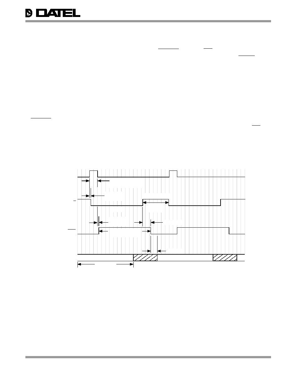
Figure 2 shows the relationship between the various input
signals. The timing shown applies over the operating
temperature range and over the operating power supply
range.
7. Re-initiating the START CONVERT (pin 16) while EOC is a
logic "1" (high) will result in a new conversion sequence.
TECHNICAL NOTES
1. Applications which are unaffected by endpoint errors or
remove them through software will use the typical connec-
tions shown in Figure 3. Remove system errors or adjust
the small initial errors of the ADS-117 to zero using the
optional external circuitry shown in Figure 4. The external
adjustment circuit has no effect on the throughput rate.
2. Always connect the analog and digital grounds to a ground
plane beneath the converter for best performance. The
analog and digital grounds are not connected to each other
internally.
3. Bypass the analog and digital supplies and the +10V
reference (pin 21) to ground with 4.7µF, 25V tantalum
electrolytic capacitors in parallel with 0.1µF ceramic
capacitors. Bypass the +10V reference (pin 21) to
ANALOG GROUND (pin 23).
4. Obtain straight binary/offset binary output coding by tying
COMP BIN (pin 18) to +5V or leaving it open. The device
has an internal pull-up resistor on this pin. To obtain
complementary binary or complementary offset binary
Figure 2. ADS-117 Timing Diagram
START
CONVERT
INTERNAL S/H
N
N+1
Acquisition Time
165ns typ.
170ns max.
10ns min.
25ns max.
EOC
10ns min.
17ns max.
Conversion Time
325ns typ.
60ns max.
Note: Scale is approximately 25ns per division.
35ns max.
OUTPUT
DATA
DATA N-1 VALID
INVALID
DATA
DATA N VALID
350ns min.
INVALID
DATA
150ns max.
50ns typ.,
30ns min., 60ns max.
Hold
Æ
Æ
ADS-117
4
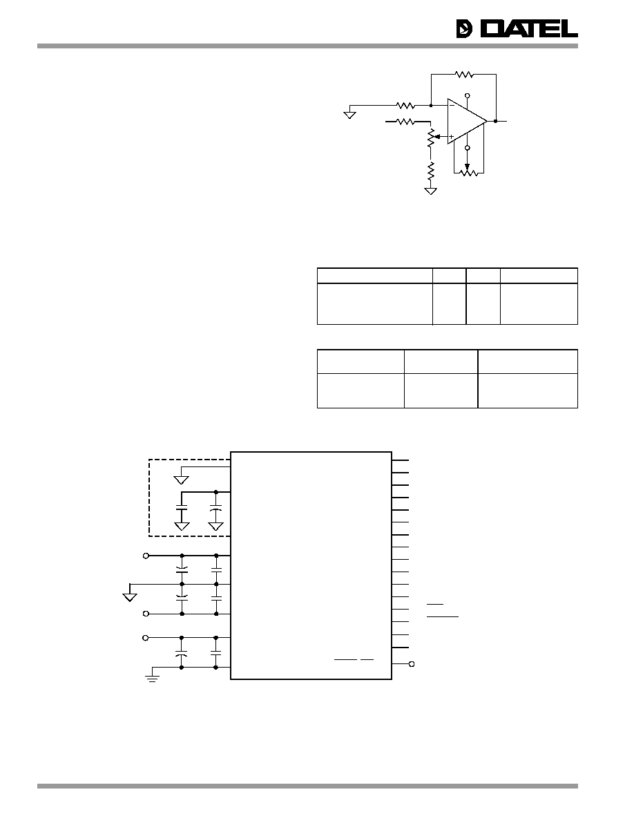
CALIBRATION PROCEDURE
1. Connect the converter per Figure 3, Figure 4, and Table 1
for the appropriate input range. Apply a pulse of 150
nanoseconds to the START CONVERT input (pin 16) at a
rate of 250kHz. This rate is chosen to reduce flicker if LED's
are used on the outputs for calibration purposes.
2. Zero Adjustments
Apply a precision voltage reference source between the
amplifier's analog input and ground. Adjust the output of the
reference source per Table 2. For unipolar, adjust the zero
trimming potentiometer so that the output code flickers
equally between 0000 0000 0000 and 0000 0000 0001 with
the pin 18 tied high (straight binary) or between 1111 1111
1111 and 1111 1111 1110 with the pin 18 tied low (comple-
mentary binary).
For bipolar operation, adjust the potentiometer such that the
code flickers equally between 1000 0000 0000 and 1000
0000 0001 with pin 18 tied high (offset binary) or between
0111 1111 1111 and 0111 1111 1110 with pin 18 tied low
(complementary offset binary).
3. Full-Scale Adjustment
Set the output of the voltage reference used in step 2 to the
value shown in Table 1. Adjust the gain trimming potentiom-
eter so that the output code flickers equally between 1111
1111 1110 and 1111 1111 1111 for pin 18 tied high or
between 0000 0000 0001 and 0000 0000 0000 for pin 18
tied low.
4. To confirm proper operation of the device, vary the precision
reference voltage source to obtain the output coding listed
in Table 3.
To Pin19
of ADS-117
≠15V
+15V
For values of R1 and R2 refer to Table 1.
R2
R1
5k
50
10k
ZERO/
OFFSET
ADJUST
SIGNAL
INPUT
GAIN
ADJUST
5k
Figure 3. ADS-117 Connection Diagram
Table 1. Input Connections (using external calibration)
INPUT RANGE
R1
R2
UNIT
0 +10V, ±5
2
2
k
0 to 5V, ±2.5V
2
6
k
0 to +2.5V, ±1.25V
2
14
k
Table 2. Zero and Gain Adjustments
Input
Zero Adjust
Gain Adjust
Range
+1/2 LSB
+FS ≠ 1 1/2 LSB
0 to +10V
+1.22mV
+9.9963V
±5V
+1.22mV
+4.9963V
Figure 4. Optional Calibration Circuit
0.1µF
4.7µF
13
14
ADS-117
19
16
12
11
10
9
8
7
6
5
4
3
2
1
15
17
BIT 1 (MSB)
BIT 2
BIT 3
BIT 4
BIT 5
BIT 6
BIT 7
BIT 8
BIT 9
BIT 10
BIT 11
BIT 12 (LSB)
EOC
ENABLE (1-12)
ANALOG INPUT
START CONVERT
+
+5V
≠15V
+15V
+
+
0.1µF
4.7µF
23
22
0.1µF
4.7µF
24
20
COMP BIN
0.1µF
+
4.7µF
21 +10V REF.
UNIPOLAR
OPERATION
18
+5V
NOTE:
BIPOLAR INPUT
For unipolar operation, ground pin 20.
For bipolar operation, connect pin 20 to pin 21.
Always bypass pin 21 as shown for both unipolar
and bipolar operation.
Æ
Æ
ADS-117
5
Table 3. Output Coding
UNIPOLAR
INPUT RANGE
OUTPUT CODING
INPUT RANGE
BIPOLAR
SCALE
0 to +10V
MSB LSB
MSB
LSB
±5V
SCALE
+FS ≠ 1 LSB
+9.9976
1111 1111 1111
0000 0000 0000
+4.9976
+FS ≠1 LSB
+7/8 FS
+8.7500
1110 0000 0000
0001 1111 1111
+3.7500
+3/4FS
+3/4 FS
+7.5000
1100 0000 0000
0011 1111 1111
+2.5000
+1/2FS
+1/2 FS
+5.0000
1000 0000 0000
0111 1111 1111
0.0000
0
+1/4 FS
+2.5000
0100 0000 0000
1011 1111 1111
≠2.5000
≠1/2FS
+1/8 FS
+1.2500
0010 0000 0000
1101 1111 1111
≠3.7500
≠3/4FS
+1 LSB
+0.0024
0000 0000 0001
1111 1111 1110
≠4.9976
≠FS+1LSB
0
0.0000
0000 0000 0000
1111 1111 1111
≠5.0000
≠FS
STRAIGHT BIN.
COMP. BINARY
OFF. BINARY
COMP. OFF. BIN.
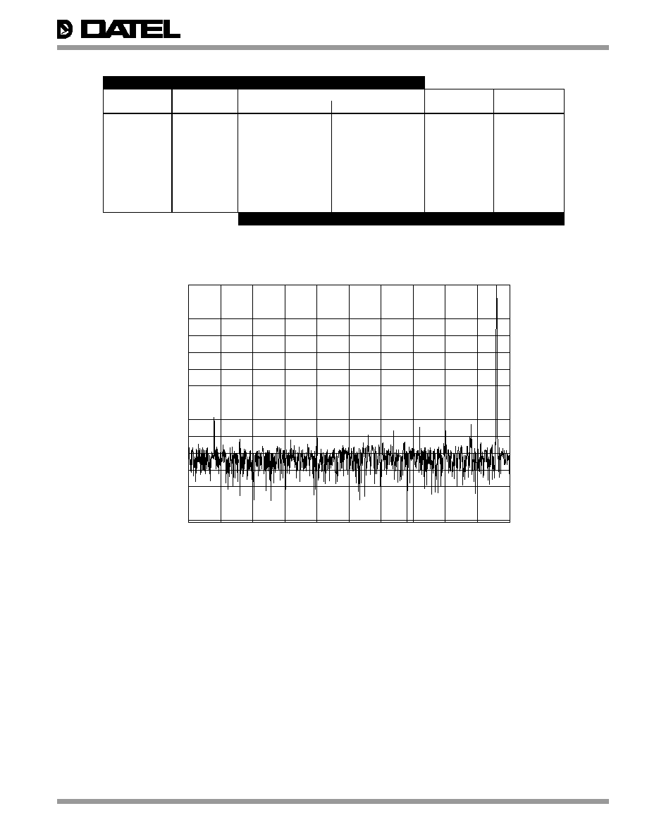
Figure 5. FFT Analysis of ADS-117
0
≠10
≠20
≠30
≠40
≠50
≠60
≠70
≠80
≠90
≠100
≠110
≠120
≠130
≠140
Frequency (MHz)
(fs = 2MHz, fin = 980kHz, Vin = ≠0.5dB, 4,096-point FFT)
A
m
p
l
i
t
u
d
e
R
e
l
a
t
i
v
e
t
o
F
u
l
l
S
c
a
l
e
(
d
B
)
0 0.1 0.2 0.3 0.4 0.5 0.6 0.7 0.8 0.9 1.0