 | –≠–ª–µ–∫—Ç—Ä–æ–Ω–Ω—ã–π –∫–æ–º–ø–æ–Ω–µ–Ω—Ç: ADS-325A | –°–∫–∞—á–∞—Ç—å:  PDF PDF  ZIP ZIP |
IN N O VA T IO N a n d E X C E L L E N C E
Æ
Æ
GENERAL DESCRIPTION
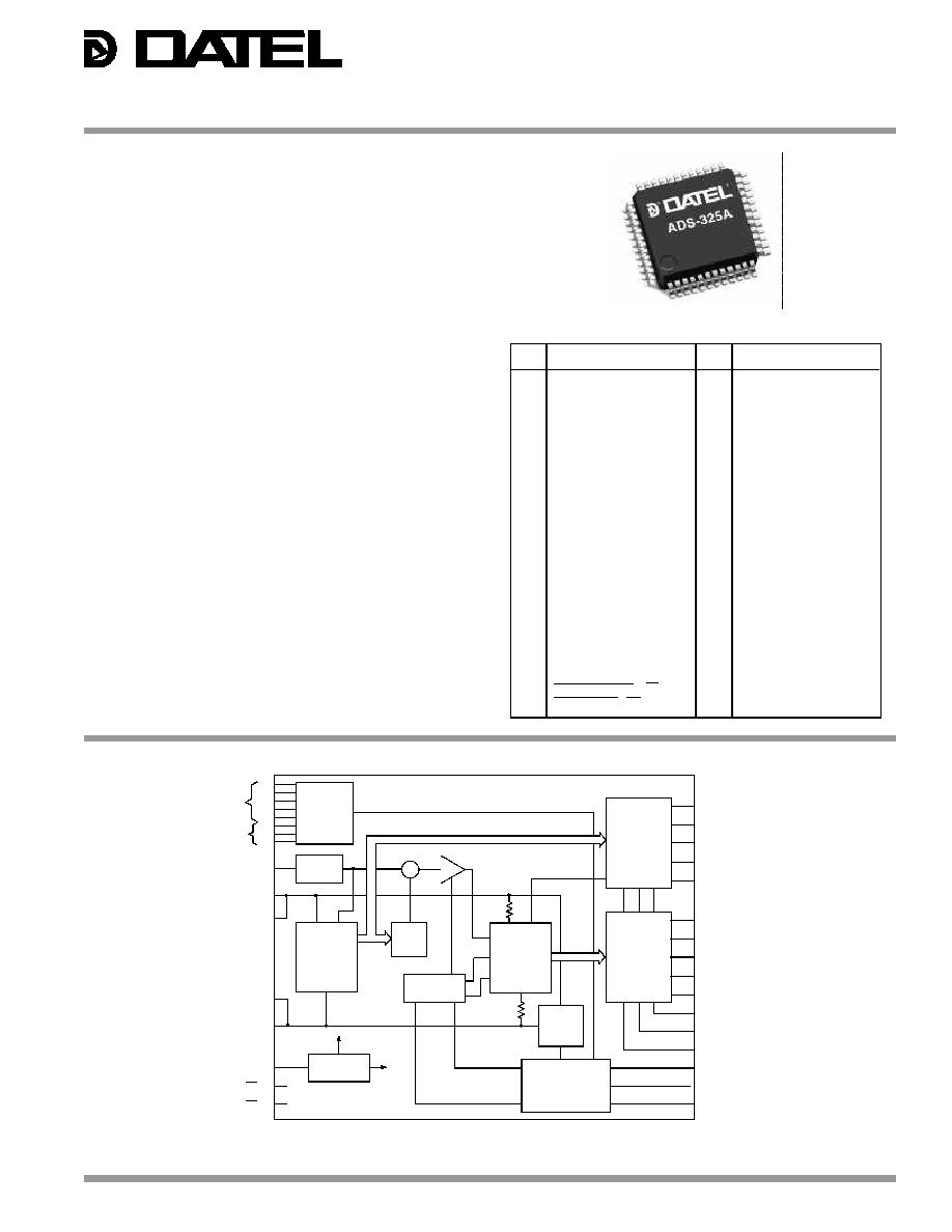
DATEL's ADS-325A is a low power, 10-bit, 20MHz, CMOS
sampling A/D converter. Its small 48 pin plastic LQFP package
contains a S/H amplifier, a 3-state output register, linearity
calibration circuitry, and all necessary control logic. Only two
external reference voltages, an A/D clock and a few digital
inputs are required. The A/D clock may be applied with 50%
duty cycle.
The excellent dynamic performance includes a spurious free
dynamic range of 65dB and a signal-to-noise ratio with
distortion of 54dB with a 3MHz input. ADS-325A is capable of
operating from a single +5V power supply and typically
consumes only 150mW. It can also operate from a +5V analog
V
S
with +3.3V digital V
S
enabling an interface with 3.3V logic
circuitry. The ADS-325A is ideally suited for high quality video/
CCD imaging applications.
FEATURES
∑ 10-bit, 20MHz sampling
∑ ±1LSB max. differential nonlinearity
∑ Internal calibration circuit
∑ Internal S/H amplifier
∑ 70MHz input bandwidth
∑ TTL/CMOS compatible in-out logic
∑ Latched three-state output data
∑ Single +5V supply
∑ Low 150mW power dissipation
∑ Small 48 pin LQFP package
∑ Low cost
Figure 1. ADS-325A Functional Block Diagram
INPUT/OUTPUT CONNECTIONS
PIN
FUNCTION
1
BIT 10 (LSB)
2
BIT 9
3
BIT 8
4
BIT 7
5
BIT 6
6
DIGITAL GROUND (DGND)
7
+DV
S
(Digital)
8
BIT 5
9
BIT 4
10
BIT 3
11
BIT 2
12
BIT 1 (MSB)
13
TEST PIN
14
TEST SIGNAL IN
15
RESET
16
DIGITAL GROUND (DGND)
17
SELECT (SEL)
18
+AVS (Analog)
19
TEST MODE
20
LINV
21
MINV
22
A/D CLOCK
23
OUTPUT ENABLE (OE)
24
CHIP ENABLE (CE)
PIN
FUNCTION
48
DIGITAL GROUND (DGND)
47
NO CONNECTION
46
NO CONNECTION
45
+DV
S
(Digital)
44
ANALOG GROUND (AGND)
43
ANALOG GROUND (AGND)
42
TEST SIGNAL IN
41
CALIBRATION (CAL)
40
NO CONNECTION
39
ANALOG INPUT (V
IN
)
38
TEST SIGNAL OUT
37
TEST SIGNAL IN
36
ANALOG GROUND (AGND)
35
REFERENCE BOTTOM (
VRB
)
34
REFERENCE BOTTOM (V
RB
)
33
NO CONNECTION
32
NO CONNECTION
31
NO CONNECTION
30
REFERENCE TOP (V
RT
)
29
REFERENCE TOP (V
RT
)
28
ANALOG GROUND (AGND)
27
ANALOG GROUND (AGND)
26
+AVS (Analog)
25
+AVS (Analog)
ADS-325A
10-Bit, 20MHz
Sampling A/D Converter
DATEL, Inc., Mansfield, MA 02048 (USA)
∑
Tel: (508) 339-3000, (800) 233-2765 Fax: (508) 339-6356
∑
Email: sales@datel.com
∑
Internet: www.datel.com
1 BIT 10 (LSB)
2 BIT 9
3 BIT 8
4 BIT 7
5 BIT 6
8 BIT 5
9 BIT 4
10 BIT 3
11 BIT 2
12 BIT 1 (MSB)
35
34
29
30
39
23
24
22
21 MINV
20 LINV
19 TEST MODE
17 SEL
15 RESET
V
RT
V
IN
A/D CLOCK
CE
OE
S/H AMP
COARSE
COMPARISON
AND
ENCODE
DAC
CALIBRATION
UNIT
TIMING GEN.
FINE
LATCH
COARSE
CORRECTION
AND
LATCH
FINE
COMPARISON
AND
ENCODE
41 CAL
x8
+
V
RB
AGND
44
25
43
27
28
36
18
26
SENSE
AMP
#1
+AV
S
AUTOCALIBRATION
PULSE
GENERATOR
SENSE
AMP
#2
V
RT
V
RB

Æ
Æ
ADS-325A
PERFORMANCE (CONT.)
MIN.
TYP.
MAX.
UNITS
Spurious Free Dynamic Range
f
IN
= 100kHz
--
60
--
dB
f
IN
= 500kHz
--
59
--
dB
f
IN
= 1MHz
--
60
--
dB
f
IN
= 3MHz
--
65
--
dB
f
IN
= 7MHz
--
50
--
dB
f
IN
= 10MHz
--
49
--
dB
POWER REQUIREMENTS
Power Supply Voltage
+AV
S
+4.75
+5.0
+5.25
Volts
+DV
S
+3.0
--
+5.25
Volts
|DGND ≠ AGND |
--
--
100
mV
Supply Current
Analog, +AI
S
20
27
34
mA
Digital, +DI
S
--
3
5
mA
Standby Current (CE = "1")
Analog, +AI
S
--
--
1
mA
Digital, +DI
S
--
--
1
µA
Power Dissipation
--
150
--
mW
PHYSICAL/ENVIRONMENTAL
Operating Temperature Range
≠20
--
+75
∞C
Storage Temperature Range
≠55
--
+150
∞C
Weight
0.2 grams
Package
48-pin plastic LQFP
ANALOG INPUTS
MIN.
TYP.
MAX.
UNITS
Input Voltage Range, V
IN
+2 to +4
Volts
Input Current
V
IN
= +4V
--
40
50
µA
V
IN
= +2V
≠50
≠40
--
µA
Capacitance, C
IN
--
9
--
pF
Bandwidth (≠1dB)
--
70
--
MHz
REFERENCE
Reference Input Voltage
V
RT
--
+4
+4.6
Volts
V
RB
+1.8
+2
--
Volts
Input Current
I
RT
5
7
11
mA
I
RB
≠11
≠7
≠5
mA
Offset Voltage
V
RT
+40
+90
+140
mV
V
RB
≠120
≠70
≠20
mV
Resistance (V
RT
≠ V
RB
)
180
280
380
DIGITAL INPUTS
Input Voltage
V
IH,
Logic "1"
+2.3
--
--
Volts
V
IL,
Logic "0"
--
--
+0.8
Volts
Input Current
I
IH
, Logic Loading "1"
--
--
5
µA
I
IL
, Logic Loading "0"
--
--
5
µA
A/D Clock Pulse Width
T
PW1
25
--
--
ns
T
PW0
25
--
--
ns
DIGITAL OUTPUTS
Output Logic Current
I
OH,
Logic "1"
≠3.5
--
--
mA
I
OL,
Logic "0"
3.5
--
--
mA
Leak Current at OE = "1"
--
--
1
µA
3-State Enable Time, T
PZE
10
15
20
ns
3-State Disable Time, T
PEZ
20
25
30
ns
Data Delay, T
DL
(C
L
= 20pF)
8
13
18
ns
PERFORMANCE
Resolution
10
--
--
Bits
Max. Throughput Rate
20
--
--
MHz
Min. Throughput Rate
--
--
0.5
MHz
Integral Linearity Error
--
±1.3
±2
LSB
Differential Linearity Error
--
±0.5
±1
LSB
Differential Gain Error
--
1.0
--
%
Differential Phase Error
--
0.3
--
Degrees
Aperture Delay, Tsd
2
4
6
ns
SNR & Distortion
f
IN
= 100kHz
--
53
--
dB
f
IN
= 500kHz
--
52
--
dB
f
IN
= 1MHz
--
53
--
dB
f
IN
= 3MHz
--
54
--
dB
f
IN
= 7MHz
--
47
--
dB
f
IN
= 10MHz
--
45
--
dB
ABSOLUTE MAXIMUM RATINGS (T
A
= +25∞C)
FUNCTIONAL SPECIFICATIONS
(Typical at f
S
= 20MHz, +AV
S
= +5V, +DV
S
= +3.3V, V
RB
= +2.0V, V
RT
= +4.0V,
and T
A
= +25∞C unless otherwise specified.)
Footnotes:
+DV
S
= Max., V
IH
= +DV
S
+DV
S
= Max., V
IL
= 0V
OE = AGND, +DV
S
= Min.,
V
OH
= +DV
S
-0.5V
OE = AGND, +DV
S
= Min.,
V
OL
= 0.4V
OE = +AV
S
, +DV
S
= Max.,
V
OH
= +DV
S
, and V
OL
= 0V
Hi-Z to Active, asynchronous with clock.
Active to Hi-Z, asynchronous with clock.
Fin = 1kHz
NTSC 401RE mod. ramp, fc = 14.3MHz
TECHNICAL NOTES
1. Caution to ESD: Since the ADS-325A is a CMOS device,
precautions against static electricity should be taken.
2. +AV
S
and +DV
S
: While the unit has separate pins for both
the analog supply (+AV
S
) and the digital supply (+DV
S
), a
time skew between supplying (or removing) both +AV
S
and
+DV
S
may cause a latch-up problem. DATEL recommends
using a common power supply for both +AV
S
and +DV
S
to
avoid latch-up conditions. It is possible to use +3.3V for
+DV
S
along with +5V for +AV
S
. Compared to the singe +5V
supply application, there will be no significant difference in
performance. However, special care should be taken to
minimize the time skew between +AV
S
and +DV
S
when
turning on/off.
3. PC board layout: To obtain fully specified performance
careful attention to PC board layout is required. Place large
ground planes on the board and connect both analog and
digital grounds at one point right beneath the converter. In
the case where the grounds are tied at a location distant
from the converter, the voltage difference between the
grounds must be within 100mV. Tie all ground pins directly
to the appropriate ground plane beneath the converter.
Bypass +AV
S
and +DV
S
pins to ground using 10µF
tantalum capacitors in parallel with 0.1µF ceramic
capacitors at locations as close to the unit as possible.
4. Reference Input: Two external voltage references are
required for the two reference inputs VRT (pin 29, 30) and
VRB (pin 34, 35). Typically, these are +4V for VRT and +2V
PARAMETERS
LIMITS
UNITS
Supply Voltages (+AV
S
and +DV
S
)
0 to +7
Volts
Reference Voltage (V
RT
and V
RB
)
≠0.5 to +AV
S
+0.5
Volts
Input Voltage, Analog (V
IN
)
≠0.5 to +AV
S
+0.5
Volts
Input Voltage, Digital (V
IH
and V
IL
)
≠0.5 to +AV
S
+0.5
Volts
Output Voltage, Digital (V
OH
and V
OL
)
≠0.5 to +DV
S
+0.5
Volts
2
ADS-325A
Æ
Æ
for VRB, which give an analog input range of +2V to +4V.
The reference voltages must be within the following
limitations:
+AVS ≠ 0.4V > = VRT > VRB >= +1.8V, and
VRT ≠ VRB > =1.8V
Stability of the reference will directly affect the accuracy of
the A/D conversion. In this sense, the reference sources
must be capable of driving more than 10mA. Also, the VRT
and VRB pins should be bypassed to analog ground with
0.1µF ceramic capacitors placed as close to the pins as
possible.
5. Analog Input: ADS-325A has a broad input bandwidth of
70MHz (@≠1dB) with only 9pF of input capacitance at its
analog input. The analog input should be driven by a high
speed buffer amplifier with sufficient current drive.
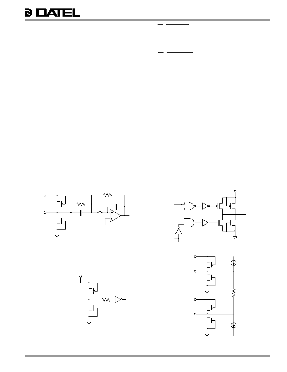
6. Digital Inputs: All digital input pins including A/D clock input
are CMOS compatible. Each of these pins has an internal
overvoltage protection circuit with diodes as shown in Figure
2 (Equivalent circuit diagrams).
7. Control Logic Inputs: ADS-325A has several control logic
input pins. Functions of these pins are described in the
following:
TEST MODE (pin 19), MINV (pin 21), LINV (pin 20)
These three pins select the output data format. With a
combination of these input states the output data takes any
form of binary, complementary binary, 2's compliment, or
certain test pattern. Refer to Table 1 (Output coding) and
Table 2 (Truth table).
3
CE (Chip Enable, pin 24)
For normal operation the input to this pin should be logic
low. Input high applied to the pin puts the unit into standby
mode. In standby mode the unit dissipates only a few milli-
watts or less.
OE (Output Enable, pin 23)
Input logic low applied to this pin enables the three-state
output bits (Bit 1 to Bit 10). Input high disables the outputs.
RESET (pin 15)
This pin can be used to re-initiate start-up calibration.
Normally connect this pin to logic high. See Calibration
Function for more details.
CAL (Calibration Input, pin 41)
This pin is the input for an external calibration pulse. See
Calibration Function for more details.
SEL (Select, pin 17)
Applying logic high to this pin allows use of the internal auto
calibration function and blocks out the external pulse from
the CAL input. Inputting logic low to the pin disables the
internal cal function and allows usage of the external cal
pulses.
8. Test IN/OUT pins: Test signal input/output pins are used in
the production process. The test signal output pins (pin 13,
38) should normally be left open. Tie the test signal input pin
42 to +AV
S
and the pins 14 and 37 to +AV
S
or AGND.
9. Three-state output buffer: A/D output buffer (BIT 1 to
BIT 10) is a three-state register controlled by the OE pin.
The output logic high level is dependent on +DV
S
.
SEL, CLK, CAL, RESET, OE, CE, Test Mode,
LINV and MINV Inputs
Digital Data Outputs
Figure 2. Equivelant Circuits
Reference Input
Analog Signal Input
AGND
39
+AV
S
V
IN
+AV
S
AGND
RESET 15
SELECT 17
TEST MODE 19
LINV 20
MINV 21
CLOCK 22
OUTPUT ENABLE (OE) 23
CHIP ENABLE (CE) 24
CAL. PULSE IN (CAL) 41
DGND
+DV
S
OUTPUT
BIT
AGND
29
30
34
35
V
RT
V
RB
AGND
+AV
S
+AV
S
Æ
Æ
ADS-325A
Figure 3. Calibration Timing Diagram
4
Table 1. Digital Output Coding
CALIBRATION FUNCTION
To achieve its superior linearity ADS-325A has an internal
calibration circuit with a built-in calibration pulse generation
circuit and an input pin for an external calibration pulse. The
calibration circuit consists of three D/A converters, a pattern
generator and an averaging circuit. With either internal or
external calibration pulses applied to the calibration circuit, the
circuit senses an offset of the x8 gain amplifier and two
reference biases supplied from the V
RT
and the V
RB
to a fine
comparator/encoder block, and compensates them using the
three DACs.
With a single negative going calibration pulse a unit cycle of
calibration is completed. It is initiated with the negative going
edge of the calibration pulse and takes seven A/D clock
periods to be completed. Due to the fact that this calibration
cycle occupies the lower comparator for four A/D clock periods
the lower five bits of the output data remain constant through 4
clock cycles after the completion of the cycle. Figure 3 shows
the timing for the calibration cycle.
A sequence of seven unit calibration cycles initiated by seven
calibration pulses, completes a single calibration process. The
number of calibration processes required depends on the
condition of the device and on the stability of the references
and the power. Even in worst case, 80 calibration processes
done by 560 calibration pulses are enough to finish the whole
calibration.
There are three modes of the calibration function. These are:
a. Start-up calibration function
b. Internal auto-calibration function
c. External calibration function
For operation in modes a. and b. the ADS-325A has a built-in
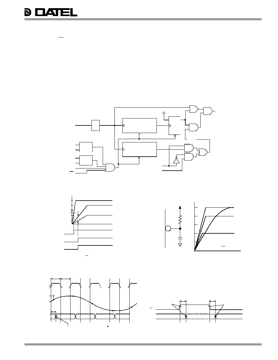
calibration pulse generation circuit. Figure 4a. illustrates a
simplified block diagram of this circuit.
Start-up Calibration Function
At power-up of the unit the initial calibration process requires
over 600 calibration pulses. The internal start-up calibration
function automatically generates these pulses when power is
first applied to the ADS-325A. To initiate the start-up
calibration, the following five conditions must be met. See
Figure 4b.
1. The supply voltage +AV
S
must be at least 2.5 Volts higher
than AGND.
2. The voltage difference between V
RT
and V
RB
must be at
least 1 Volt.
3. The RESET pin (pin 15) must be set high.
4. The CE pin (pin 24) must be set low.
5. Condition 1 must be met before condition 2.
Once all of the above conditions have been met, the calibration
pulses are generated by counting 16 A/D clock cycles on a
14-bit counter until closing the gate when the carry-out occurs.
The time required for the start-up calibration is determined by
the following formula:
Start-up Calibration Time = 1/f
CLK
x 16 x 16,384
where f
CLK
is the frequency of the A/D clock input. For example,
a clock frequency of 14.3MHz requires a calibration time of
18.3ms.
Analog
Digital Output Code
Input Voltage
Step
MSB
LSB
3.998V
1023
11
1111
1111
3.996V
1022
11
1111
1110
:
:
:
3.000V
512
10
0000
0000
2.998V
511
01
1111
1111
:
:
:
2.002V
1
00
0000
0001
2.000V
0
00
0000
0000
TEST
Digital Output
MODE
LINV
MINV
MSB
LSB
1
0
0
PP
PPPP
PPPP
1
1
0
PN
NNNN
NNNN
1
0
1
NP
PPPP
PPPP
1
1
1
NN
NNNN
NNNN
0
1
1
10
1010
1010
0
0
1
11
0101
0101
0
1
0
00
1010
1010
0
0
0
01
0101
0101
Table 2. Digital Output Truth Table
TEST MODE = 1, LINV = 0, MINV = 0
P = Positive True; N = Negative True (inverted)
7 Clock Cycles
10ns
>
A/D CLOCK
CAL
BIT 1 TO BIT 5
(MSB)
BIT 6 TO BIT 10
(LSB)
1 Clock Cycle
>
N
N≠1
N≠2
N≠3
N+1 N+2 N+3
N+5
N+4
N≠1
N≠2
N≠3
4 Clock Cycles
N
N+5
ADS-325A
Æ
Æ
5
Re-initiating the Start-up Calibration
The start-up calibration function can be re-initiated at any time
desired after the power and the references are supplied. Apply
a positive pulse to CE pin (pin 24) or a negative pulse to
RESET pin (pin 15). The pulse width of these pulses must be
equal to or wider than one A/D clock cycle. Also due to this
feature, you can make sure of a proper start-up calibration at
power-up by making a C-R delay connection with the RESET
pin as shown in Figure 4c.
Using Start-up Calibration Function Only
Internal and external calibration functions need not be
employed after start-up calibration. To use only the start-up
calibration function, connect the SEL pin (pin 17) to AGND and
the CAL pin (pin 14) to +AV
S
or AGND.
Auto Calibration Function
After the start up calibration is completed, the internal
calibration function can periodically and automatically generate
calibration pulses when the auto calibration mode is enabled.
To enable this function connect the SEL pin (pin 17) and the
CAL pin (pin 41) to +AV
S
. In this mode a 24-bit counter is
counted with every 16 A/D clock cycles and the carry-out is
used as the calibration pulse. The period of the calibration
pulse generated is as follows:
Period of Auto-calibration pulse = 1/f
CLK
x 16 x 16,777,216
For the case when the A/D clock frequency is 14.3MHz, the
calibration pulse generation cycle is 18.8 seconds. Since a
single calibration process is performed once every seven
pulses, the total calibration cycle is approximately
132 seconds.
Figure 4b. Conditions for Start-Up Calibration
Figure 4c. Start-up Calibration using RESET
Figure 4a Internal Calibration Pulse Generation Circuit
Figure 5. ADS-325A Timing Diagrams
14-BIT COUNTER
CO
CLR
CLR
D
Q
24-BIT COUNTER
CO
CLR
SEL
CAL
SENSE
AMP #1
SENSE
AMP #2
1/16
RESET
CE
V
RT
V
RB
+AV
S
AGND
A/D CLOCK
+AV
S
OUT
CLOCK
ANALOG
INPUT
= SAMPLING POINT
OUTPUT
DATA
N≠3
N≠2
N≠1
N
N
N+1
N+2
N+3
N+4
+1.65V
T
Tsd
ACTIVE
HIGH IMPEDENCE
ACTIVE
T
PEZ
OUTPUT
DATA
OUTPUT
ENABLE (OE)
PW1
T
PW0
T
PZE
T
DL
+1.65V (+DV = +3.3V)
+2.5V (+DV = +5.0V)
S
S
+1.65V (+DV = +3.3V)
+2.5V (+DV = +5.0V)
S
S
+1.65V (+DV = +3.3V)
+2.5V (+DV = +5.0V)
S
S
0
+2.5
+5
SENSE AMP #1
SENSE AMP #2
CLR
+AV
S
V
RT
V
RB
TIME
VOLTS
RESET = HIGH, CE = LOW
1V
+AV
S
15
5V
+AV
S
V
RT
RESET
V
RB
CE = "L"