 | –≠–ª–µ–∫—Ç—Ä–æ–Ω–Ω—ã–π –∫–æ–º–ø–æ–Ω–µ–Ω—Ç: ADS-933MC | –°–∫–∞—á–∞—Ç—å:  PDF PDF  ZIP ZIP |
PIN
FUNCTION
PIN
FUNCTION
1
+3.2V REF. OUT
40
NO CONNECTION
2
UNIPOLAR
39
NO CONNECTION
3
ANALOG INPUT
38
+5V ANALOG SUPPLY
4
ANALOG GROUND
37
≠5V SUPPLY
5
OFFSET ADJUST
36
ANALOG GROUND
6
GAIN ADJUST
35
COMP. BITS
7
DIGITAL GROUND
34
OUTPUT ENABLE
8
FIFO/DIR
33
OVERFLOW
9
FIFO READ
32
EOC
10
FSTAT1
31
+5V DIGITAL SUPPLY
11
FSTAT2
30
DIGITAL GROUND
12
START CONVERT
29
BIT 1 (MSB)
13
BIT 16 (LSB)
28
BIT 1 (MSB)
14
BIT 15
27
BIT 2
15
BIT 14
26
BIT 3
16
BIT 13
25
BIT 4
17
BIT 12
24
BIT 5
18
BIT 11
23
BIT 6
19
BIT 10
22
BIT 7
20
BIT 9
21
BIT 8
FEATURES
∑
16-bit resolution
∑
3MHz sampling rate
∑
Functionally complete
∑
No missing codes over full military temperature range
∑
Edge-triggered
∑
±5V supplies, 1.85 Watts
∑
Small, 40-pin, ceramic TDIP
∑
85dB SNR, ≠84dB THD
∑
Ideal for both time and frequency-domain applications
16-Bit, 3MHz
Sampling A/D Converters
Æ
Æ
I N N O V A T I O N a n d E X C E L L E N C E
GENERAL DESCRIPTION
The low-cost ADS-933 is a 16-bit, 3MHz sampling A/D
converter. This device accurately samples full-scale input
signals up to Nyquist frequencies with no missing codes. The
dynamic performance of the ADS-933 has been optimized to
achieve a signal-to-noise ratio (SNR) of 85dB and a total
harmonic distortion (THD) of ≠84dB.
Packaged in a 40-pin TDIP, the functionally complete
ADS-933 contains a fast-settling sample-hold amplifier, a
subranging (two-pass) A/D converter, an internal reference,
timing/control logic, and error-correction circuitry. Digital input
and output levels are TTL. The ADS-933 only requires the
rising edge of the start convert pulse to operate.
Requiring only ±5V supplies, the ADS-933 dissipates 1.85
Watts. The device is offered with a bipolar (±2.75V) analog
input range and a unipolar 0 to ≠5.5V input range. Models are
available for use in either commercial (0 to +70∞C) or military (≠
55 to +125∞C) operating temperature ranges. A proprietary, auto-
calibrating, error-correcting circuit enables the device to achieve
specified performance over the full military temperature range.
Typical applications include medical imaging, radar, sonar,
communications and instrumentation.
INPUT/OUTPUT CONNECTIONS
ADS-933
DATEL, Inc., Mansfield, MA 02048 (USA)
∑
Tel: (508)339-3000, (800)233-2765 Fax: (508) 339-6356
∑
E-mail: sales@datel.com
∑
Internet: www.datel.com
Figure 1. ADS-933 Functional Block Diagram
PRELIMINARY PRODUCT DATA
3
-
S
T
A
T
E
O
U
T
P
U
T
R
E
G
I
S
T
E
R
29 BIT 1 (MSB)
28 BIT 1 (MSB)
27 BIT 2
26 BIT 3
25 BIT 4
24 BIT 5
23 BIT 6
22 BIT 7
21 BIT 8
20 BIT 9
19 BIT 10
18 BIT 11
17 BIT 12
16 BIT 13
15 BIT 14
14 BIT 15
13 BIT 16 (LSB)
TIMING AND
CONTROL LOGIC
GAIN ADJUST 6
+3.2V REF. OUT 1
OFFSET ADJUST 5
EOC 32
+5V ANALOG SUPPLY 38
+5V DIGITAL SUPPLY 31
≠5V SUPPLY 37
ANALOG GROUND 4, 36
DIGITAL GROUND 7, 30
NO CONNECTION 39, 40
C
U
S
T
O
M
G
A
T
E
A
R
R
A
Y
POWER AND GROUNDING
2
-
P
A
S
S
A
N
A
L
O
G
-
T
O
-
D
I
G
I
T
A
L
C
O
N
V
E
R
T
E
R
S/H
GAIN
ADJUST
CKT.
OFFSET
ADJUST
CKT.
PRECISION
+3.2V REFERENCE
ANALOG INPUT 3
START CONVERT 12
COMP. BITS 35
10 FSTAT1
11 FSTAT2
8 FIFO/DIR
9 FIFO/READ
34 OUTPUT ENABLE
33 OVERFLOW
UNIPOLAR 2
OFFSET ADJUST 5
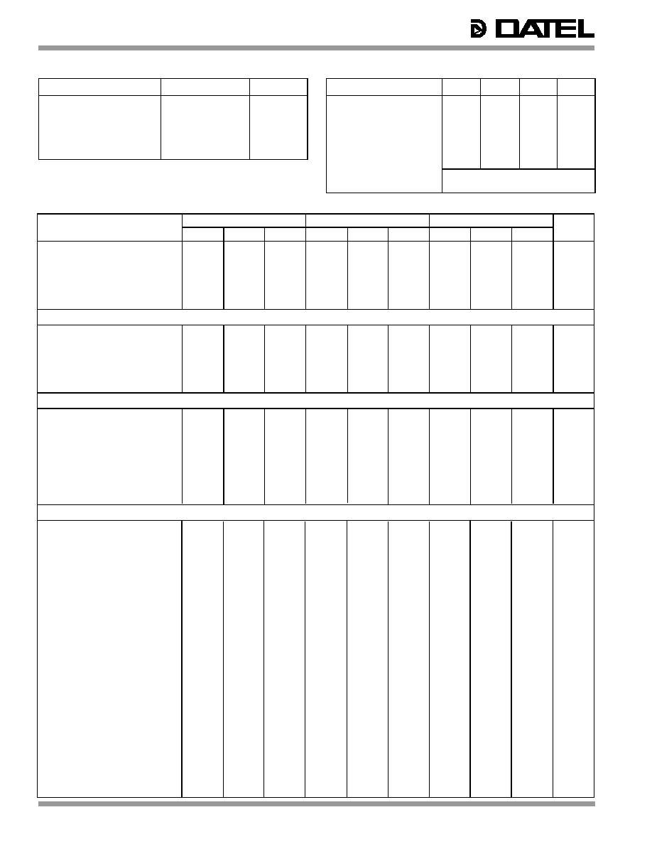
ADS-933
Æ
Æ
2
PARAMETERS
MIN.
TYP.
MAX.
UNITS
Operating Temp. Range, Case
ADS-933MC
0
--
+70
∞C
ADS-933MM
≠55
--
+125
∞C
Thermal Impedance
jc
--
4
--
∞C/Watt
ca
--
18
--
∞C/Watt
Storage Temperature Range
≠65
--
+150
∞C
Package Type
40-pin, metal-sealed, ceramic TDIP
Weight
0.56 ounces (16 grams)
ABSOLUTE MAXIMUM RATINGS
PARAMETERS
LIMITS
UNITS
+5V Supply (Pins 31, 38)
0 to +6
Volts
≠5V Supply (Pin 37)
0 to ≠6
Volts
Digital Inputs (Pins 8, 9, 12, 34, 35) ≠0.3 to +V
DD
+0.3
Volts
Analog Input (Pin 3)
±5
Volts
Lead Temperature (10 seconds)
+300
∞C
PHYSICAL/ENVIRONMENTAL
FUNCTIONAL SPECIFICATIONS
(T
A
= +25∞C, ±V
CC
= ±5V, +V
DD
= +5V, 3MHz sampling rate, and a minimum 3 minute warm-up unless otherwise specified.)
+25∞C
0 to +70∞C
≠55 to +125∞C
ANALOG INPUT
MIN.
TYP.
MAX.
MIN.
TYP.
MAX.
MIN.
TYP.
MAX.
UNITS
Input Voltage Range
Unipolar
--
0 to ≠5.5
--
--
0 to ≠5.5
--
--
0 to ≠5.5
--
Volts
Bipolar
--
±2.75
--
--
±2.75
--
--
±2.75
--
Volts
Input Resistance Pin 3
655
687
--
655
687
--
655
687
--
Input ResistancePin 2
418
426
--
418
426
--
418
426
--
Input Capacitance
--
10
15
--
10
15
--
10
15
pF
DIGITAL INPUTS
Logic Levels
Logic "1"
+2.0
--
--
+2.0
--
--
+2.0
--
--
Volts
Logic "0"
--
--
+0.8
--
--
+0.8
--
--
+0.8
Volts
Logic Loading "1"
--
--
+20
--
--
+20
--
--
+20
µA
Logic Loading "0"
--
--
≠20
--
--
≠20
--
--
≠20
µA
Start Convert Positive Pulse Width
20
50
--
20
50
--
20
50
--
ns
STATIC PERFORMANCE
Resolution
--
16
--
--
16
--
--
16
--
Bits
Integral Nonlinearity (f
in
= 10kHz)
--
±1
--
--
±1.5
--
--
±2
--
LSB
Differential Nonlinearity (f
in
= 10kHz)
≠0.95
±0.5
+1.0
≠0.95
±0.5
+1.0
≠0.95
±0.5
+1.5
LSB
Full Scale Absolute Accuracy
--
±0.15
±0.3
--
±0.3
±0.5
--
±0.5
±0.8
%FSR
Bipolar Zero Error (Tech Note 2)
--
±0.1
±0.2
--
±0.2
±0.4
--
±0.4
±0.6
%FSR
(Unipolar offset spec same as Bipolar zero)
Bipolar Offset Error (Tech Note 2)
--
±0.1
±0.2
--
±0.2
±0.4
--
±0.4
±0.6
%FSR
Gain Error (Tech Note 2)
--
±0.15
±0.3
--
±0.3
±0.5
--
±0.5
±0.8
%
No Missing Codes (f
in
= 10kHz)
16
--
--
16
--
--
16
--
--
Bits
DYNAMIC PERFORMANCE
Peak Harmonics (≠0.5dB)
dc to 500kHz
--
--
81
--
≠86
--
--
≠86
--
dB
500kHz to 1MHz
--
≠84
80
--
≠84
--
--
≠84
--
dB
Total Harmonic Distortion (≠0.5dB)
dc to 500kHz
--
≠84
80
--
≠84
--
--
≠84
--
dB
500kHz to 1MHz
--
≠83
80
--
≠83
--
--
≠83
--
dB
Signal-to-Noise Ratio
(w/o distortion, ≠0.5dB)
dc to 500kHz
81
85
--
--
85
--
--
85
--
dB
500kHz to 1MHz
81
85
--
--
85
--
--
85
--
dB
Signal-to-Noise Ratio
(& distortion, ≠0.5dB)
dc to 500kHz
78
82
--
--
82
--
--
82
--
dB
500kHz to 1MHz
78
81
--
--
81
--
--
81
--
dB
Noise
--
80
--
--
80
--
--
80
--
µVrms
Two-Tone Intermodulation
Distortion (f
in
= 200kHz,
240kHz, f
s
= 3MHz, ≠0.5dB)
--
≠87
--
--
≠87
--
--
≠87
--
dB
Input Bandwidth (≠3dB)
Small Signal (≠20dB input)
--
9.8
--
--
9.8
--
--
9.8
--
MHz
Large Signal (≠0.5dB input)
--
10.2
--
--
10.2
--
--
10.2
--
MHz
Feedthrough Rejection
(f
in
= 1MHz)
--
90
--
--
90
--
--
90
--
dB
Slew Rate
--
±120
--
--
±120
--
--
±120
--
V/µs
Aperture Delay Time
--
+8
--
--
+8
--
--
+8
--
ns
Aperture Uncertainty
--
3
--
--
3
--
--
3
--
psrms
S/H Acquisition Time
( to ±0.001%FSR, 5.5V step)
--
180
--
--
180
--
--
180
--
ns
ADS-933
Æ
Æ
3
+25∞C
0 TO +70∞C
≠55 TO +125∞C
DYNAMIC PERFORMANCE
(Cont.)
MIN.
TYP.
MAX.
MIN.
TYP.
MAX.
MIN.
TYP.
MAX.
UNITS
ANALOG OUTPUT
Overvoltage Recovery Time
--
--
333
--
--
333
--
--
333
ns
A/D Conversion Rate
3
--
--
3
--
--
3
--
--
MHz
Internal Reference
Voltage
3.15
+3.2
--
--
+3.2
--
--
+3.2
--
Volts
Drift
--
±30
--
--
±30
--
--
±30
--
ppm/∞C
External Current
--
5
--
--
5
--
--
5
--
mA
DIGITAL OUTPUTS
Logic Levels
Logic "1"
+2.4
--
--
+2.4
--
--
+2.4
--
--
Volts
Logic "0"
--
--
+0.4
--
--
+0.4
--
--
+0.4
Volts
Logic Loading "1"
--
--
≠4
--
--
≠4
--
--
≠4
mA
Logic Loading "0"
--
--
+4
--
--
+4
--
--
+4
mA
Output Coding
Offset Binary / Complementary Offset Binary / Two's Complement / Complementary Two's Complement
POWER REQUIREMENTS
Power Supply Ranges }
+5V Supply
+4.75
+5.0
+5.25
+4.75
+5.0
+5.25
+4.9
+5.0
+5.25
Volts
≠5V Supply
≠4.75
≠5.0
≠5.25
≠4.75
≠5.0
≠5.25
≠4.9
≠5.0
≠5.25
Volts
Power Supply Currents
+5V Supply
--
+220
260
--
+220
260
--
+220
260
mA
≠5V Supply
≠140
≠150
--
≠140
≠150
--
≠140
≠150
--
mA
Power Dissipation
--
1.85
2.0
--
1.85
2.0
--
1.85
2.0
Watts
Power Supply Rejection
--
--
±0.07
--
--
±0.07
--
--
±0.07
%FSR/%V
Footnotes:
Effective bits is equal to:
All power supplies must be on before applying a start convert pulse. All
supplies and the clock (START CONVERT) must be present during
warm-up periods. The device must be continuously converting during
this time.
When COMP. BITS (pin 35) is low, logic loading "0" will be ≠350µA.
A 3MHz clock with a 50nsec positive pulse width is used for all
production testing. See Timing Diagram for more details.
6.02
(SNR + Distortion) ≠ 1.76 + 20 log
Full Scale Amplitude
Actual Input Amplitude
This is the time required before the A/D output data is valid once the
analog input is back within the specified range.
The minimum supply voltages of +4.9V and ≠4.9V for ±V
DD
are required for
≠55∞C operation only. The minimum limits are +4.75V and ≠4.75V when
operating at +125∞C.
TECHNICAL NOTES
1. Obtaining fully specified performance from the ADS-933
requires careful attention to pc-card layout and power
supply decoupling. The device's analog and digital ground
systems are connected to each other internally. For optimal
performance, tie all ground pins (2, 4, 7, 30 and 36) directly
to a large analog ground plane beneath the package.
Bypass all power supplies and the +3.2V reference output
to ground with 4.7µF tantalum capacitors in parallel with
0.1µF ceramic capacitors. Locate the bypass capacitors as
close to the unit as possible.
2. The ADS-933 achieves its specified accuracies without the
need for external calibration. If required, the device's small
initial offset and gain errors can be reduced to zero using
the adjustment circuitry shown in Figure 2. When using this
circuitry, or any similar offset and gain calibration hardware,
make adjustments following warm-up. To avoid interaction,
always adjust offset before gain. Tie pins 5 and 6 to
ANALOG GROUND (pin 4) if not using offset and gain
adjust circuits.
3. Pin 35 (COMP. BITS) is used to select the digital output
coding format of the ADS-933. See Tables 2a and 2b.
When this pin has a TTL logic "0" applied, it complements
all of the ADS-933's digital outputs.
When pin 35 has a logic "1" applied, the output coding is
complementary offset binary. Applying a logic "0" to pin
35 changes the coding to offset binary. Using the MSB
output (pin 29) instead of the MSB output (pin 28) changes
the respective output codings to complementary two's
complement and two's complement.
Pin 35 is TTL compatible and can be directly driven with
digital logic in applications requiring dynamic control over
its function. There is an internal pull-up resistor on pin 35
allowing it to be either connected to +5V or left open when
a logic "1" is required.
4. To enable the three-state outputs, connect OUTPUT
ENABLE (pin 34) to a logic "0" (low). To disable, connect
pin 34 to a logic "1" (high).
ADS-933
Æ
Æ
4
DELAY
PIN
TRANSITION
MIN.
TYP.
MAX.
UNITS
Direct mode to FIFO enabled
8
≠
10
20
ns
FIFO enabled to direct mode
8
≠
10
20
ns
FIFO READ to output data valid
9
≠
≠
40
ns
FIFO READ to status update when changing
from <half full (1 word) to empty
9
≠
≠
20
ns
FIFO READ to status update when changing
from
half full (8 words) to <half full (7 words)
9
≠
≠
110
ns
FIFO READ to status update when changing
from full (16 words) to
half full (15 words)
9
≠
≠
190
ns
Falling edge of EOC to status update when writing
first word into empty FIFO
32
≠
≠
190
ns
Falling edge of EOC to status update when
changing FIFO from <half full (7 words) to
32
≠
≠
110
ns
half full (8 words)
Falling edge of EOC to status update when filling
FIFO with 16th word
32
≠
≠
28
ns
INTERNAL FIFO OPERATION
The ADS-933 contains an internal, user-initiated, 18-bit, 16-
word FIFO memory. Each word in the FIFO contains the 16
data bits as well as the MSB and overflow bits. Pins 8 (FIFO/
DIR) and 9 (FIFO READ) control the FIFO's operation. The
FIFO's status can be monitored by reading pins 10 (FSTAT1)
and 11 (FSTAT2).
When pin 8 (FIFO/DIR) has a logic "1" applied, the FIFO is
inserted into the digital data path. When pin 8 has a logic
"0" applied, the FIFO is transparent and the output data goes
directly to the output three-state register (whose operation is
controlled by pin 34 (ENABLE)). Read and write commands
to the FIFO are ignored when the ADS-933 is operated in
the "direct" mode. It takes a maximum of 20ns to switch the
FIFO in or out of the ADS-933's digital data path.
FIFO Write and Read Modes
Once the FIFO has been enabled (pin 8 high), digital data is
automatically written to it, regardless of the status of FIFO
READ (pin 9). Assuming the FIFO is initially empty, it will
accept data (18-bit words) from the next 16 consecutive A/D
conversions. As a precaution, pin 9 (which controls the
FIFO's READ function) should not be low when data is first
written to an empty FIFO.
When the FIFO is initially empty, digital data from the first
conversion (the "oldest" data) appears at the output of the
FIFO immediately after the first conversion has been completed
and remains there until the FIFO is read.
If the output three-state register has been enabled (logic "0"
applied to pin 34), data from the first conversion will appear at
the output of the ADS-933. Attempting to write a 17th word to a
full FIFO will result in that data, and any subsequent
conversion data, being lost.
Once the FIFO is full (indicated by FSTAT1 and FSTAT2 both
equal to "1"), it can be read by dropping the FIFO READ line
(pin 9) to a logic "0" and then applying a series of 15 rising
edges to the read line. Since the first data word is already
present at the FIFO output, the first read command (the first
rising edge applied to FIFO READ) will bring data from the
second conversion to the output. Each subsequent read
command/rising edge brings the next word to the output lines.
After the 15th rising edge brings the 16th data word to the FIFO
output, the subsequent falling edge on READ will update the
status outputs (after a 20ns maximum delay) to FSTAT1 = 0,
FSTAT2 = 1 indicating that the FIFO is empty.
If a read command is issued after the FIFO empties, the last
word (the 16th conversion) will remain present at the outputs.
FIFO Reset Feature
At any time, the FIFO can be reset to an empty state by putting
the ADS-933 into its "direct" mode (logic "0" applied to pin 8,
FIFO/DIR) and also applying a logic "0" to the FIFO READ line
(pin 9). The empty status of the FIFO will be indicated by
FSTAT1 going to a "0" and FSTAT2 going to a "1". The status
outputs change 40ns after applying the control signals.
FIFO Status, FSTAT1 and FSTAT2
Monitor the status of the data in the FIFO by reading the two
status pins, FSTAT1 (pin 10) and FSTAT2 (pin 11).
CONTENTS
FSTAT1
FSTAT2
Empty (0 words)
0
1
<half full (<8 words)
0
0
half-full or more (
8 words)
1
0
Full (16 words)
1
1
Table 1. FIFO Delays
1
0
0
1
1
0
0
1
0
1
0
1
0
1
1
0
1
0
5. Applying a start convert pulse while a conversion is in
progress (EOC = logic "1") will initiate a new and probably
inaccurate conversion cycle. Data from both the inter-
rupted and subsequent conversions will be invalid.
6. Do not enable/disable or complement the output bits or
read from the FIFO during the conversion process (from the
rising edge of EOC to the falling edge of EOC).
7. The OVERFLOW bit (pin 33) switches from 0 to 1 when the
input voltage exceeds that which produces an output of all
1's or when the input equals or exceeds the voltage that
produces all 0's. When COMP BITS is activated, the above
conditions are reversed.
ADS-933
Æ
Æ
5
LED's to the digital outputs and performing adjustments until
certain LED's "flicker" equally between on and off. Other
approaches employ digital comparators or microcontrollers to
detect when the outputs change from one code to the next.
For the ADS-933, offset adjusting is normally accomplished
when the analog input is 0 minus Ω LSB (≠42µV). See Table
2b for the proper bipolar output coding.
Gain adjusting is accomplished when the analog input is at
nominal full scale minus 1Ω LSB's (+2.749874V).
Note: Connect pin 5 to ANALOG GROUND (pin 4) for
operation without zero/offset adjustment. Connect pin 6 to
pin 4 for operation without gain adjustment.
Zero/Offset Adjust Procedure
1. Apply a train of pulses to the START CONVERT input (pin
12) so that the converter is continuously converting.
2. For zero/offset adjust, apply ≠42µV to the ANALOG INPUT
(pin 3).
3. Adjust the offset potentiometer until the code flickers
between 1000 0000 0000 0000 and 0111 1111 1111 1111
with pin 35 tied high (complementary offset binary) or
between 0111 1111 1111 1111 and 1000 0000 0000 0000
with pin 35 tied low (offset binary).
4. Two's complement coding requires using BIT 1 (MSB) (pin
29). With pin 35 tied low, adjust the trimpot until the output
code flickers between all 0's and all 1's.
Gain Adjust Procedure
1. For gain adjust, apply +2.749874V to the ANALOG INPUT
(pin 3).
2. Adjust the gain potentiometer until all output bits are 0's and
the LSB flickers between a 1 and 0 with pin 35 tied high
(complementary offset binary) or until all output bits are 1's
and the LSB flickers between a 1 and 0 with pin 35 tied low
(offset binary).
3. Two's complement coding requires using BIT 1 (MSB)
(pin 29). With pin 35 tied low, adjust the gain trimpot until
the output code flickers equally between 0111 1111 1111
1111 and 0111 1111 1111 1110.
4. To confirm proper operation of the device, vary the applied
input voltage to obtain the output coding listed in Table 2b.
1111 1111 1111 1111
LSB "1" to "0"
1110 0000 0000 0000
1100 0000 0000 0000
1000 0000 0000 0000
0111 1111 1111 1111
0100 0000 0000 0000
0010 0000 0000 0000
0000 0000 0000 0001
LSB "0" to "1"
0000 0000 0000 0000
OFFSET BINARY
MSB
LSB
MSB
LSB
MSB
LSB
MSB
LSB
+FS ≠1 LSB
+FS ≠1 1/2 LSB
+3/4 FS
+1/2 FS
0
≠1 LSB
≠1/2 FS
≠3/4 FS
≠FS +1 LSB
≠FS + 1/2 LSB
≠FS
OUTPUT CODING
INPUT
RANGE
±2.75V
+2.749916
+2.749874
+2.062500
+1.375000
0.000000
≠0.000084
≠1.375000
≠2.062500
≠2.749916
≠2.749958
≠2.750000
0000 0000 0000 0000
LSB "0" to "1"
0001 1111 1111 1111
0011 1111 1111 1111
0111 1111 1111 1111
1000 000
000 0000
1011 1111 1111 1111
1101 1111 1111 1111
1111 1111 1111 1110
LSB "1" to "0"
1111 1111 1111 1111
COMP. OFF. BIN.
0111 1111 1111 1111
LSB "1" to "0"
0110 0000 0000 0000
0100 0000 0000 0000
0000 0000 0000 0000
1111 1111 1111 1111
1100 0000 0000 0000
1010 0000 0000 0000
1000 0000 0000 0001
LSB "0" to "1"
1000 0000 0000 0000
TWO'S COMP.
1000 0000 0000 0000
LSB "0" to "1"
1001 1111 1111 1111
1011 1111 1111 1111
1111 1111 1111 1111
0000 0000 0000 0000
0011 1111 1111 1111
0101 1111 1111 1111
0111 1111 1111 1110
LSB "1" to "0"
0111 1111 1111 1111
COMP. TWO'S COMP.
BIPOLAR
SCALE
Table 2b. Output Coding
Complementary Offset Binary
1
Offset Binary
0
Complementary Two's Complement
1
(Using MSB, pin 29)
Two's Complement
0
(Using MSB, pin 29)
OUTPUT FORMAT
PIN 35 LOGIC LEVEL
Table 2a. Setting Output Coding Selection (Pin 35)
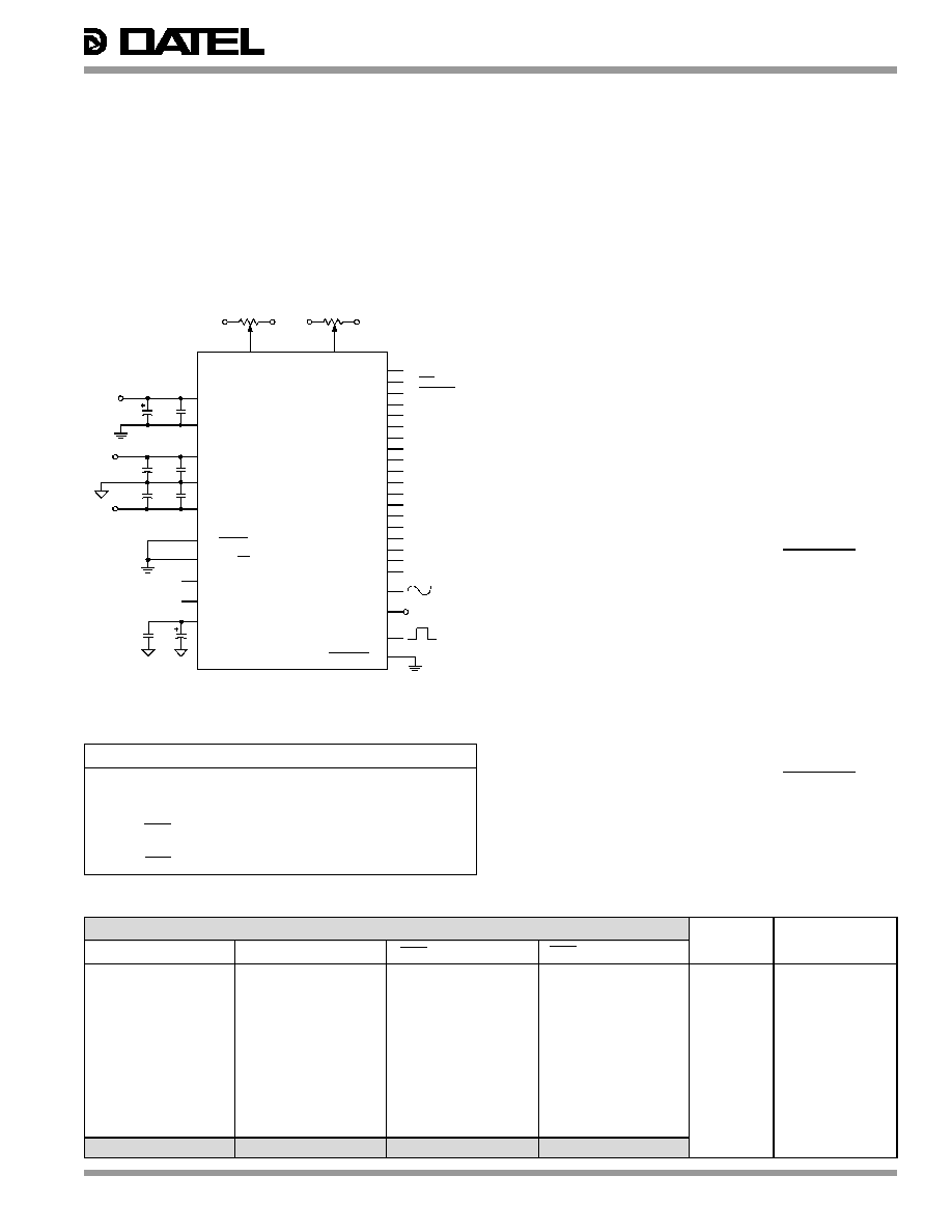
Figure 2. Connection Diagram
CALIBRATION PROCEDURE
Connect the converter per Figure 2. Any offset/gain
calibration procedures should not be implemented until the
device is fully warmed up. To avoid interaction, adjust offset
before gain. The ranges of adjustment for the circuits in
Figure 2 are guaranteed to compensate for the ADS-933's
initial accuracy errors and may not be able to compensate for
additional system errors.
A/D converters are calibrated by positioning their digital
outputs exactly on the transition point between two adjacent
digital output codes. This is accomplished by connecting
ADS-933
20k
33
32
29
28
27
26
25
24
23
22
21
20
19
18
17
16
15
14
13
OVERFLOW
EOC
BIT 1 (MSB)
BIT 1 (MSB)
BIT2
BIT 3
BIT 4
BIT 5
BIT 6
BIT 7
BIT 8
BIT 9
BIT 10
BIT 11
BIT 12
BIT 13
BIT 14
BIT 15
BIT 16 (LSB)
ANALOG
GROUND
DIGITAL
GROUND
0.1µF
4.7µF
0.1µF
COMP. BITS
4.7µF
+3.2V
REF. OUT
FIFO READ
31
7, 30
35
1
9
+5V
DIGITAL
≠5V
+5V
OFFSET
ADJUST
GAIN
ADJUST
5
6
3
0.1µF
4.7µF
2, 4, 36
37
0.1µF
4.7µF
38
+
+
20k
≠5V
+5V
≠5V
+5V ANALOG
12
START CONVERT
ANALOG INPUT
34
ENABLE
8
FIFO/DIR
10
FSTAT1
11
FSTAT2
+5V
+5V
+5V
≠5V