 | –≠–ª–µ–∫—Ç—Ä–æ–Ω–Ω—ã–π –∫–æ–º–ø–æ–Ω–µ–Ω—Ç: ADS-935MC | –°–∫–∞—á–∞—Ç—å:  PDF PDF  ZIP ZIP |
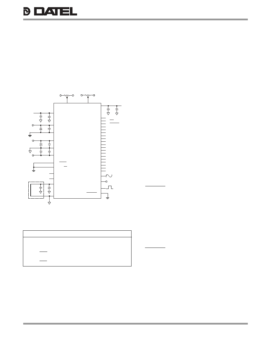
PIN FUNCTION PIN FUNCTION
1 +3.2V REF. OUT 40 +12V/+15V
2 UNIPOLAR 39 ≠12V/≠15V
3 ANALOG INPUT 38 +5V ANALOG SUPPLY
4 ANALOG GROUND 37 ≠5V SUPPLY
5 OFFSET ADJUST 36 ANALOG GROUND
6 GAIN ADJUST 35 COMP. BITS
7 DIGITAL GROUND 34 OUTPUT ENABLE
8 FIFO/DIR 33 OVERFLOW
9 FIFO READ 32 EOC
10 FSTAT1 31 +5V DIGITAL SUPPLY
11 FSTAT2 30 DIGITAL GROUND
12 START CONVERT 29 BIT 1 (MSB)
13 BIT 16 (LSB) 28 BIT 1 (MSB)
14 BIT 15 27 BIT 2
15 BIT 14 26 BIT 3
16 BIT 13 25 BIT 4
17 BIT 12 24 BIT 5
18 BIT 11 23 BIT 6
19 BIT 10 22 BIT 7
20 BIT 9 21 BIT 8
FEATURES
∑
16-bit resolution
∑
5MHz sampling rate
∑
Functionally complete
∑
No missing codes over full military temperature range
∑
Edge-triggered
∑
±5V, ±12V or ±15V supplies, 3.0 Watts
∑
Small, 40-pin, ceramic TDIP
∑
83dB SNR, ≠86dB THD
∑
Ideal for both time and frequency-domain applications
16-Bit, 5MHz
Sampling A/D Converters
GENERAL DESCRIPTION
The ADS-935 is a 16-bit, 5MHz sampling A/D converter. This
device accurately samples full-scale input signals up to Nyquist
frequencies with no missing codes. The dynamic performance
of the ADS-935 has been optimized to achieve a signal-to-noise
ratio (SNR) of 83dB and a total harmonic distortion (THD) of
≠86dB.
Packaged in a 40-pin TDIP, the functionally complete
ADS-935 contains a fast-settling sample-hold amplifi er, a
subranging (two-pass) A/D converter, an internal reference,
timing/control logic, and error-correction circuitry. Digital input
and output levels are TTL. The ADS-935 only requires the
rising edge of the start convert pulse to operate.
Requiring ±5V supplies and either ±12v or ±15V supplies the
ADS-935 dissipates 3.0 Watts. The device is offered with a
bipolar (±2.75V) or a unipolar (0 to ≠5.5V) analog input range.
Models are available for use in either commercial (0 to +70∞C)
or military (≠55 to +125∞C) operating temperature ranges.
A proprietary, auto-calibrating, error-correcting circuit enables
the device to achieve specifi ed performance over the full
military temperature range. Typical applications include medical
imaging, radar, sonar, communications and instrumentation.
INPUT/OUTPUT CONNECTIONS
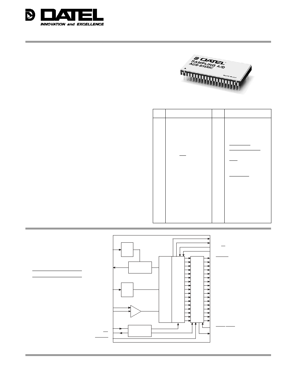
ADS-935
DATEL, Inc., Mansfi eld, MA 02048 (USA)
∑
Tel: (508)339-3000, (800)233-2765 Fax: (508)339-6356
∑
Email: sales@datel.com
∑
Internet: www.datel.com
Figure 1. ADS-935 Functional Block Diagram
PRELIMINARY PRODUCT DATA
3
-
ST
ATE
OUTP
UT REGI
STE
R
29 BIT
1
(MSB)
28 BIT
1
(MSB)
27 BIT
2
26 BIT
3
25 BIT
4
24 BIT
5
23 BIT
6
22 BIT
7
21 BIT
8
20 BIT
9
19 BIT
10
18 BIT
11
17 BIT
12
16 BIT
13
15 BIT
14
14 BIT
15
13 BIT 16 (LSB)
TIMING AND
CONTROL LOGIC
GAIN ADJUST 6
+3.2V REF. OUT 1
OFFSET ADJUST 5
EOC 32
CUST
O
M GAT
E
A
RRAY
2
-
PASS ANAL
OG-
TO-
D
I
G
I
T
AL CONVERTER
S/H
GAIN
ADJUST
CKT.
OFFSET
ADJUST
CKT.
PRECISION
+3.2V REFERENCE
ANALOG INPUT 3
START CONVERT 12
COMP. BITS 35
10 FSTAT1
11 FSTAT2
8 FIFO/DIR
9 FIFO/READ
34 OUTPUT ENABLE
33 OVERFLOW
Æ
Æ
POWER AND GROUNDING
+5V ANALOG SUPPLY
38
+5V DIGITAL SUPPLY
31
≠5V SUPPLY
37
ANALOG GROUND
4, 36
DIGITAL GROUND
7, 30
≠12/≠15V ANALOG SUPPLY 39
+12/+15V ANALOG SUPPLY 40
UNIPOLAR 2
ADS-935
2
Æ
Æ
+25∞C 0 to +70∞C ≠55 to +125∞C
ANALOG INPUT MIN. TYP. MAX. MIN. TYP. MAX. MIN. TYP. MAX. UNITS
Input Voltage Range
Unipolar -- 0 to ≠5.5V -- --
0 to ≠5.5V
--
--
0 to ≠5.5V
--
Volts
Bipolar -- ±2.75 -- -- ±2.75 -- -- ±2.75 -- Volts
Input Resistance (Pin 3) -- 400 -- --
400
--
--
400
--
(Pin 2) -- 480 -- -- 480 -- -- 480 --
Input Capacitance -- 10 15 --
10
15
--
10
15
pF
DIGITAL INPUTS
Logic Levels
Logic "1" +2.0 -- -- +2.0 -- -- +2.0 -- -- Volts
Logic "0" -- -- +0.8 -- -- +0.8 -- -- +0.8 Volts
Logic Loading "1" -- -- +20 -- -- +20 -- -- +20 µA
Logic Loading "0" -- -- ≠20 -- -- ≠20 -- -- ≠20 µA
Start Convert Positive Pulse Width 20 50 -- 20 50 -- 20 50 -- ns
STATIC PERFORMANCE
Resolution -- 16 -- -- 16 -- -- 16 -- Bits
Integral Nonlinearity -- ±1 -- -- ±1.5 -- -- ±2 -- LSB
Differential Nonlinearity (f
in
= 10kHz) ≠0.95 ±0.5 +1.0 ≠0.95 ±0.5 +1.0 ≠0.95 ±0.5 +1.5 LSB
Full Scale Absolute Accuracy -- ±0.15 ±0.3 -- ±0.3 ±0.5 -- ±0.5 ±0.8 %FSR
Bipolar Zero Error (Tech Note 2) -- ±0.1 ±0.2 -- ±0.2 ±0.4 -- ±0.4 ±0.6 %FSR
Bipolar Offset Error (Tech Note 2) -- ±0.1 ±0.2 -- ±0.2 ±0.4 -- ±0.4 ±0.6 %FSR
Gain Error (Tech Note 2) -- ±0.15 ±0.3 -- ±0.3 ±0.5 -- ±0.5 ±0.8 %
No Missing Codes (f
in
= 10kHz) 16 -- -- 16 -- -- 16 -- -- Bits
DYNAMIC PERFORMANCE
Peak Harmonics (≠0.5dB)
dc to 500kHz -- ≠87 -- -- ≠87 -- -- ≠82 -- dB
500kHz to 2.45MHz -- ≠82 -- -- ≠82 -- -- ≠78 -- dB
Total Harmonic Distortion (≠0.5dB)
dc to 500kHz -- ≠86 -- -- ≠86 -- -- ≠81 -- dB
500kHz to 2.45MHz -- ≠81 -- -- ≠81 -- -- ≠77 -- dB
Signal-to-Noise Ratio
(w/o distortion, ≠0.5dB)
dc to 500kHz -- 83 -- -- 83 -- -- 80 -- dB
500kHz to 2.45MHz -- 82 -- -- 82 -- -- 75 -- dB
Signal-to-Noise Ratio
(& distortion, ≠0.5dB)
dc to 500kHz -- 80 -- -- 80 -- -- 78 -- dB
500kHz to 2.45MHz -- 77 -- -- 77 -- -- 75 -- dB
Noise -- 80 -- -- 80 -- -- 80 -- µVrms
Two-Tone Intermodulation
Distortion (f
in
= 200kHz,
240kHz, f
s
= 5MHz, ≠0.5dB) -- ≠87 -- -- ≠87 -- -- ≠87 -- dB
Input Bandwidth (≠3dB)
Small Signal (≠20dB input) -- TBD -- -- TBD -- -- TBD -- MHz
Large Signal (≠0.5dB input) -- TBD -- -- TBD -- -- TBD -- MHz
Feedthrough Rejection
(f
in
= 1MHz) -- 90 -- -- 90 -- -- 90 -- dB
Slew Rate -- TBD -- -- TBD -- -- TBD -- V/µs
Aperture Delay Time -- TBD -- -- TBD -- -- TBD -- ns
Aperture Uncertainty -- TBD -- -- TBD -- -- TBD -- ps rms
S/H Acquisition Time
( to ±0.001%FSR, 5.5V step) -- 80 -- -- 80 -- -- 90 -- ns
Overvoltage Recovery Time -- TBD -- -- TBD -- -- TBD -- ns
A/D Conversion Rate 5 -- -- 5 -- -- 5 -- -- MHz
PARAMETERS MIN. TYP. MAX. UNITS
Operating Temp. Range, Case
ADS-935MC 0 -- +70 ∞C
ADS-935MM ≠55 -- +125 ∞C
Thermal Impedance
jc -- 4 -- ∞C/Watt
ca -- 18 -- ∞C/Watt
Storage Temperature Range ≠65 -- +150 ∞C
Package Type 40-pin, metal-sealed, ceramic TDIP
Weight 0.56 ounces (16 grams)
ABSOLUTE MAXIMUM RATINGS
PARAMETERS LIMITS UNITS
+5V Supply (Pins 31, 38) 0 to +6 Volts
≠5V Supply (Pin 37) 0 to ≠6 Volts
+12V/+15V Supply (pin 40) 0 to +16V Volts
≠12V/≠15V Supply (pin 39) 0 to +16V Volts
Digital Inputs (Pins 8, 9, 12, 34, 35) ≠0.3 to +V
DD
+0.3 Volts
Analog Input (Pin 3) ±5 Volts
Lead Temperature (10 seconds) +300 ∞C
PHYSICAL/ENVIRONMENTAL
FUNCTIONAL SPECIFICATIONS
(T
A
= +25∞C, ±V
CC
= ±12/15V, +V
DD
= ±5V, 5MHz sampling rate, and a minimum 3 minute warm-up unless otherwise specifi ed.)
ADS-935
3
Æ
Æ
+25∞C 0 TO +70∞C ≠55 TO +125∞C
DYNAMIC PERFORMANCE
(Cont.)
MIN. TYP. MAX. MIN. TYP. MAX. MIN. TYP. MAX. UNITS
ANALOG OUTPUT
Internal Reference
Voltage -- +3.2 -- -- +3.2 -- -- +3.2 -- Volts
Drift -- ±30 -- -- ±30 -- -- ±30 -- ppm/∞C
External Current -- 5 -- -- 5 -- -- 5 -- mA
DIGITAL OUTPUTS
Logic Levels
Logic "1" +2.4 -- -- +2.4 -- -- +2.4 -- -- Volts
Logic "0" -- -- +0.4 -- -- +0.4 -- -- +0.4 Volts
Logic Loading "1" -- -- ≠4 -- -- ≠4 -- -- ≠4 mA
Logic Loading "0" -- -- +4 -- -- +4 -- -- +4 mA
Output Coding (Offset) Binary / Complementary (Offset) Binary / Two's Complement / Complementary Two's Complement
POWER REQUIREMENTS
Power Supply Ranges
+5V Supply +4.75 +5.0 +5.25 +4.75 +5.0 +5.25 +4.9 +5.0 +5.25 Volts
≠5V Supply ≠4.75 ≠5.0 ≠5.25 ≠4.75 ≠5.0 ≠5.25 ≠4.9 ≠5.0 ≠5.25 Volts
+12V Supply +11.5 +12.0 +12.5 +11.5 +12.0 +12.5 +11.5 +12.0 +12.5 Volts
≠12V Supply ≠11.5 ≠12.0 ≠12.5 ≠11.5 ≠12.0 ≠12.5 ≠11.5 ≠12.0 ≠12.5 Volts
+15V Supply +14.5 +15.0 +15.5 +14.5 +15.0 +15.5 +14.5 +15.0 +15.5 Volts
≠15V Supply ≠14.5 ≠15.0 ≠15.5 ≠14.5 ≠15.0 ≠15.5 ≠14.5 ≠15.0 ≠15.5 Volts
Power Supply Currents
+5V Supply -- +200 -- -- +220 -- -- +220 -- mA
≠5V Supply -- ≠100 -- -- ≠150 -- -- ≠150 -- mA
≠12/15V Supply -- ≠65 -- -- ≠65 -- -- -- -- mA
+12/15V Supply -- +85 -- -- +85 -- -- -- -- mA
Power Dissipation -- 2.85 3.1 -- 2.85 3.5 -- 2.85 3.5 Watts
Power Supply Rejection -- -- ±0.07 -- -- ±0.07 -- -- ±0.07 %FSR/%V
Footnotes:
Effective bits is equal to:
All power supplies must be on before applying a start convert pulse. All
supplies and the clock (START CONVERT) must be present during warm-up
periods. The device must be continuously converting during this time.
When COMP. BITS (pin 35) is low, logic loading "0" will be ≠350µA.
A 5MHz clock with a 50nsec positive pulse width is used for all production
testing. See Timing Diagram for more details.
6.02
(SNR + Distortion) ≠ 1.76 + 20 log
Full Scale Amplitude
Actual Input Amplitude
This is the time required before the A/D output data is valid once the analog
input is back within the specifi ed range.
See table 2a, Setting Output Coding Selection.
The minimum supply voltages of +4.9V and ≠4.9V for ±V
DD
are required for
≠55∞C operation only. The minimum limits are +4.75V and ≠4.75V when
operating at +125∞C.
±12V only or ±15V only required.
TECHNICAL NOTES
1. Obtaining fully specifi ed performance from the ADS-935
requires careful attention to pc-card layout and power supply
decoupling. The device's analog and digital ground systems
are connected to each other internally. For optimal perfor-
mance, tie all ground pins (4, 7, 30 and 36) directly to a large
analog
ground plane beneath the package.
Bypass all power supplies and the +3.2V reference output to
ground with 4.7µF tantalum capacitors in parallel with 0.1µF
ceramic capacitors. Locate the bypass capacitors as close
to the unit as possible.
2. The ADS-935 achieves its specifi ed accuracies without the
need for external calibration. If required, the device's small
initial offset and gain errors can be reduced to zero using
the adjustment circuitry shown in Figure 2. When using
this circuitry, or any similar offset and gain calibration hard-
ware, make adjustments following warm-up. To avoid interac-
tion, always adjust offset before gain. Tie pins 5 and 6 to
ANALOG GROUND (pin 4) if not using offset and gain adjust
circuits.
3. Pin 35 (COMP. BITS) is used to select the digital output
coding format of the ADS-935. See Tables 2a and 2b. When
this pin has a TTL logic "0" applied, it complements all of the
ADS-935's digital outputs.
When pin 35 has a logic "1" applied, the output coding is
complementary (offset) binary. Applying a logic "0" to pin
35 changes the coding to (offset) binary. Using the MSB
output (pin 29) instead of the MSB output (pin 28) changes
the respective output codings to complementary two's
complement and two's complement.
Pin 35 is TTL compatible and can be directly driven with
digital logic in applications requiring dynamic control over
its function. There is an internal pull-up resistor on pin 35
allowing it to be either connected to +5V or left open when
a logic "1" is required.
4. To enable the three-state outputs, connect OUTPUT
ENABLE (pin 34) to a logic "0" (low). To disable, connect pin
34 to a logic "1" (high).
ADS-935
4
Æ
Æ
DELAY PIN TRANSITION MIN. TYP. MAX. UNITS
Direct mode to FIFO enabled 8 ≠ 10 20 ns
FIFO enabled to direct mode 8 ≠ 10 20 ns
FIFO READ to output data valid 9 ≠ ≠ 40 ns
FIFO READ to status update when changing
from <half full (1 word) to empty 9 ≠ ≠ 20 ns
FIFO READ to status update when changing
from
half full (8 words) to <half full (7 words)
9 ≠ ≠ 110 ns
FIFO READ to status update when changing
from full (16 words) to
half full (15 words) 9 ≠ ≠ 190 ns
Falling edge of EOC to status update when writing
fi rst word into empty FIFO 32 ≠ ≠ 190 ns
Falling edge of EOC to status update when
changing FIFO from <half full (7 words) to 32 ≠ ≠ 110 ns
half full (8 words)
Falling edge of EOC to status update when fi lling
FIFO with 16th word
32 ≠ ≠ 28 ns
INTERNAL FIFO OPERATION
The ADS-935 contains an internal, user-initiated, 18-bit,
16-word FIFO memory. Each word in the FIFO contains the 16
data bits as well as the MSB and overfl ow bits. Pins 8 (FIFO/
DIR) and 9 (FIFO READ) control the FIFO's operation. The
FIFO's status can be monitored by reading pins 10 (FSTAT1)
and 11 (FSTAT2).
When pin 8 (FIFO/DIR) has a logic "1" applied, the FIFO is
inserted into the digital data path. When pin 8 has a logic
"0" applied, the FIFO is transparent and the output data goes
directly to the output three-state register (whose operation is
controlled by pin 34 (ENABLE)). Read and write commands
to the FIFO are ignored when the ADS-935 is operated in the
"direct" mode. It takes a maximum of 20ns to switch the FIFO
in or out of the ADS-935's digital data path.
FIFO Write and Read Modes
Once the FIFO has been enabled (pin 8 high), digital data
is automatically written to it, regardless of the status of FIFO
READ (pin 9). Assuming the FIFO is initially empty, it will
accept data (18-bit words) from the next 16 consecutive A/D
conversions. As a precaution, pin 9 (which controls the FIFO's
READ function) should not be low when data is fi rst written to
an empty FIFO.
When the FIFO is initially empty, digital data from the fi rst
conversion (the "oldest" data) appears at the output of the FIFO
immediately after the fi rst conversion has been completed and
remains there until the FIFO is read.
If the output three-state register has been enabled (logic "0"
applied to pin 34), data from the fi rst conversion will appear at
the output of the ADS-935. Attempting to write a 17th word
to a full FIFO will result in that data, and any subsequent
conversion data, being lost.
Once the FIFO is full (indicated by FSTAT1 and FSTAT2 both
equal to "1"), it can be read by dropping the FIFO READ line
(pin 9) to a logic "0" and then applying a series of 15 rising
edges to the read line. Since the fi rst data word is already
present at the FIFO output, the fi rst read command (the fi rst
rising edge applied to FIFO READ) will bring data from the
second conversion to the output. Each subsequent read
command/rising edge brings the next word to the output
lines. After the 15th rising edge brings the 16th data
word to the FIFO output, the subsequent falling edge on
READ will update the status outputs (after a 20ns maximum
delay) to FSTAT1 = 0,
FSTAT2 = 1 indicating that the FIFO is empty.
If a read command is issued after the FIFO empties, the last
word (the 16th conversion) will remain present at the outputs.
FIFO Reset Feature
At any time, the FIFO can be reset to an empty state by putting
the ADS-935 into its "direct" mode (logic "0" applied to pin 8,
FIFO/DIR) and also applying a logic "0" to the FIFO READ
line (pin 9). The empty status of the FIFO will be indicated by
FSTAT1 going to a "0" and FSTAT2 going to a "1". The status
outputs change 40ns after applying the control signals.
FIFO Status, FSTAT1 and FSTAT2
Monitor the status of the data in the FIFO by reading the two
status pins, FSTAT1 (pin 10) and FSTAT2 (pin 11).
CONTENTS FSTAT1 FSTAT2
Empty (0 words) 0 1
<half full (<8 words) 0 0
half-full or more (
8 words) 1 0
Full (16 words) 1 1
Table 1. FIFO Delays
0
1
5. Applying a start convert pulse while a conversion is in
progress (EOC = logic "1") will initiate a new and probably
inaccurate conversion cycle. Data from both the interrupted
and subsequent conversions will be invalid.
6. Do not enable/disable or complement the output bits or
read from the FIFO during the conversion process (from the
rising edge of EOC to the falling edge of EOC).
7. The OVERFLOW bit (pin 33) switches from 0 to 1 when the
input voltage exceeds that which produces an output of all
1's or when the input equals or exceeds the voltage that
produces all 0's. When COMP BITS is activated, the above
conditions are reversed.
1
0
1
0
1
0
1
0
0
0
1
1
1
1
0
0
ADS-935
5
Æ
Æ
LED's to the digital outputs and performing adjustments until
certain LED's "fl icker" equally between on and off. Other
approaches employ digital comparators or microcontrollers to
detect when the outputs change from one code to the next.
For the ADS-935, offset adjusting is normally accomplished
when the analog input is 0 minus Ω LSB (≠42µV). See Table 2b
for the proper bipolar output coding.
Gain adjusting is accomplished when the analog input is
at nominal full scale minus 1Ω LSB's (+2.749874V or
≠5.499874V).
Note: Connect pin 5 to ANALOG GROUND (pin 4) for
operation without zero/offset adjustment. Connect pin 6 to
pin 4 for operation without gain adjustment.
Zero/Offset Adjust Procedure
1. Apply a train of pulses to the START CONVERT input (pin
12) so that the converter is continuously converting.
2. For zero/offset adjust, apply ≠42µV to the ANALOG INPUT
(pin 3).
3. For bipolar operation - Adjust the offset potentiometer until
the code fl ickers between 1000 0000 0000 0000 and 0111
1111 1111 1111 with pin 35 tied high (complementary offset
binary) or between 0111 1111 1111 1111 and 1000 0000
0000 0000 with pin 35 tied low (offset binary).
For unipolar operation - Adjust the offset potentiometer until
all outputs are 1's and the LSB fl ickers between 0 and 1 with
pin 35 tied high (complementary binary) or until all outputs
are 0's and the LSB fl ickers between 0 and 1 with pin 35
tied low (binary).
4. For bipolar, Two's complement coding requires using
BIT 1 (MSB) (pin 29). With pin 35 tied low, adjust the trimpot
until the output code fl ickers between all 0's and all 1's.
Gain Adjust Procedure
1. For gain adjust, for bipolar apply +2.749874V and for unipo-
lar mode 5.499874V to the ANALOG INPUT (pin 3).
2. Adjust the gain potentiometer until all output bits are 0's and
the LSB fl ickers between a 1 and 0 with pin 35 tied high
(complementary (offset) binary) or until all output bits are 1's
and the LSB fl ickers between a 1 and 0 with pin 35 tied low
((offset) binary).
3. For bipolar, Two's complement coding requires using
BIT 1 (MSB) (pin 29). With pin 35 tied low, adjust the gain
trimpot until the output code fl ickers equally between 0111
1111 1111 1111 and 0111 1111 1111 1110.
4. To confi rm proper operation of the device, vary the applied
input voltage to obtain the output coding listed in Table 2b.
Complementary (Offset) Binary 1
(Offset) Binary 0
Complementary Two's Complement 1
(Using MSB, pin 29)
Two's Complement 0
(Using MSB, pin 29)
OUTPUT FORMAT PIN 35 LOGIC LEVEL
Table 2a. Setting Output Coding Selection (Pin 35)
Figure 2. Connection Diagram
CALIBRATION PROCEDURE
Connect the converter per Figure 2. Any offset/gain calibration
procedures should not be implemented until the device is fully
warmed up. To avoid interaction, adjust offset before gain.
The ranges of adjustment for the circuits in Figure 2 are
guaranteed to compensate for the ADS-935's initial accuracy
errors and may not be able to compensate for additional
system errors.
A/D converters are calibrated by positioning their digital
outputs exactly on the transition point between two adjacent
digital output codes. This is accomplished by connecting
ADS-935
31
40
39
7, 30
35
1
2
9
6
5
3
4, 36
37
38
12
34
8
10
11
33
32
29
28
27
26
25
24
23
22
21
20
19
18
17
16
15
14
13
OVERFLOW
EOC
BIT 1 (MSB)
BIT 1 (MSB)
BIT2
BIT 3
BIT 4
BIT 5
BIT 6
BIT 7
BIT 8
BIT 9
BIT 10
BIT 11
BIT 12
BIT 13
BIT 14
BIT 15
BIT 16 (LSB)
+5V
+12/+15V
≠12/≠15V
+5V
+5V
0.1µF
0.1µF
0.1µF
4.7µF
4.7µF
4.7µF
0.1µF
4.7µF
4.7µF
0.1µF
0.1µF
4.7µF
≠5V
≠5V
+5V
+5V
+
+
+
+
+
+
≠5V
≠5V
20k
20k
ANALOG GROUND
DIGITAL GROUND
COMP. BITS
+3.2V REF. OUT
UNIPOLAR
For Bipolar
Connect for
Unipolar Model
(0 to ≠5.5V)
FIFO READ
+5V DIGITAL
OFFSET
ADJUST
GAIN
ADJUST
+5V ANALOG
START CONVERT
ANALOG INPUT
ENABLE
FIFO/DIR
FSTAT1
FSTAT2
ADS-935
6
Æ
Æ
THERMAL REQUIREMENTS
All DATEL sampling A/D converters are fully characterized and
specifi ed over operating temperature (case) ranges of 0 to
+70∞C and ≠55 to +125∞C. All room-temperature (T
A
= +25∞C)
production testing is performed without the use of heat sinks or
forced-air cooling. Thermal impedance fi gures for each device
are listed in their respective specifi cation tables.
These devices do not normally require heat sinks, however,
standard precautionary design and layout procedures should
be used to ensure devices do not overheat. The ground and
power planes beneath the package, as well as all pcb
signal runs to and from the device, should be as heavy
as possible to help conduct heat away from the package.
Electrically insulating, thermally-conductive "pads" may be
installed underneath the package. Devices should be soldered
to boards rather than "socketed", and of course, minimal air
fl ow over the surface can greatly help reduce the package
temperature.
In more severe ambient conditions, the package/junction
temperature of a given device can be reduced dramatically
(typically 35%) by using one of DATEL's HS Series heat
sinks. See Ordering Information for the assigned part number.
See page 1-183 of the DATEL Data Acquisition Components
Catalog for more information on the HS Series. Request DATEL
Application Note AN-8, "Heat Sinks for DIP Data Converters," or
contact DATEL directly, for additional information.
Figure 3. ADS-935 Timing Diagram
START
CONVERT
INTERNAL S/H
N
N+1
EOC
OUTPUT
DATA
Data N-4 Valid
Conversion Time
Hold
N+2
N+3
Acquisition Time
Data N-1 Valid
Invalid
Data
Invalid
Data
Data N-2 Valid
Data N-3 Valid
20ns typ.
125ns typ.
110ns typ.
75ns typ.
50ns typ.
20ns typ.
20ns typ.
50ns typ.
150ns typ.
NOTES:
1. Scale is approximately 20ns per didsion.fs = 5MHz
2. This device has three pipeline delays. Four start convert pulses (clock cycles) must be applied for valid data from the
fi rst conversion to appear at the output of the A/D.
1111 1111 1111 1111
LSB "1" to "0"
1110 0000 0000 0000
1100 0000 0000 0000
1000 0000 0000 0000
0111 1111 1111 1111
0100 0000 0000 0000
0010 0000 0000 0000
0000 0000 0000 0001
LSB "0" to "1"
0000 0000 0000 0000
+FS ≠1 LSB
+FS ≠1 1/2 LSB
+3/4 FS
+1/2 FS
0
≠1 LSB
≠1/2 FS
≠3/4 FS
≠FS +1 LSB
≠FS + 1/2 LSB
≠FS
INPUT
RANGE
±2.75V
+2.749916
+2.749874
+2.062500
+1.375000
0.000000
≠0.000084
≠1.375000
≠2.062500
≠2.749916
≠2.749958
≠2.750000
0000 0000 0000 0000
LSB "0" to "1"
0001 1111 1111 1111
0011 1111 1111 1111
0111 1111 1111 1111
1000 000 000 0000
1011 1111 1111 1111
1101 1111 1111 1111
1111 1111 1111 1110
LSB "1" to "0"
1111 1111 1111 1111
0111 1111 1111 1111
LSB "1" to "0"
0110 0000 0000 0000
0100 0000 0000 0000
0000 0000 0000 0000
1111 1111 1111 1111
1100 0000 0000 0000
1010 0000 0000 0000
1000 0000 0000 0001
LSB "0" to "1"
1000 0000 0000 0000
1000 0000 0000 0000
LSB "0" to "1"
1001 1111 1111 1111
1011 1111 1111 1111
1111 1111 1111 1111
0000 0000 0000 0000
0011 1111 1111 1111
0101 1111 1111 1111
0111 1111 1111 1110
LSB "1" to "0"
0111 1111 1111 1111
BIPOLAR
SCALE
Table 2b. Output Coding
0 ≠1 LSB
0 ≠1 1/2 LSB
0 ≠ 1/8 FS
0 ≠ 1/4 FS
≠1/2 FS ≠ 1/2LSB
≠1/2 LSB
≠3/4 FS
≠7/8 FS
≠FS +1 LSB
≠FS + 1/2 LSB
≠FS
INPUT
RANGE
0 to ≠5.5V
≠0.000084
≠0.000126
≠0.687500
≠1.375000
≠2.749958
≠2.750000
≠4.125000
≠4.812500
≠5.499916
≠5.499958
≠5.500000
UNIPOLAR
SCALE
MSB LSB
MSB LSB
MSB LSB
MSB LSB
OFFSET BINARY COMP. OFF. BIN.
TWO'S COMP.
COMP. TWO'S COMP.
COMP. BINARY
BINARY
COMP. TWO'S COMP.
TWO'S COMP.
ADS-935
7
Æ
Æ
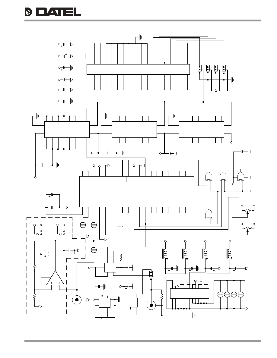
Figure 4. ADS-935 Evaluation Board Schematic.
20k
R4
1
2
3
U2
9
8
7
6
5
4
3
2
11
1
19
18
17
16
15
14
13
12
10
20
74HCT573
UUT
B6
B7
B8
B9
B10
B11
+5VD
DGND
MSB
B2
B3
B4
B5
B12
B13
B14
B15
LSB
START
ADS-935
FSTAT2
FSTAT1
+12/+15V
≠12/≠15V
+5VA
-5VA
AGND
COMP
ENABLE
OF
EOC
READ
FIFO/DIR
DGND
GAIN
OFFSET
AGND
ANA IN
+3.2VREF
U6
1
2
3
4
5
6
7
8
9
10
11
12
13
14
15
16
17
18
19
20
21
22
23
24
25
26
27
28
29
30
31
32
33
34
35
36
37
38
39
40
U1
12
11
13
8
9
10
74HCT74
2.2µF
C13
33
31
29
27
25
23
21
19
17
15
13
11
9
7
5
3
1
34
32
30
28
26
24
22
20
18
16
14
12
10
8
6
4
2
P1
FST2
START
FST1
B16
FIF/DIR
B15
READ
B14
N.C.
B13
COMPLIM
B12
ENABLE
B11
DGND
B10
DGND
B9
DGND
B8
DGND
B7
DGND
B6
DGND
B5
DGND
B4
EOC
B3
OVRFLW
B2
B1B MSB
B1(MSB)
2.2µF
C11
0.1µF
C20
U4
9
8
7
6
5
4
3
2
11
1
19
18
17
16
15
14
13
12
10
20
74HCT573
0.1µF
C15
33pF
C10
1
2
0.1µF
C18
0.1µF
C3
2.2µF
C1
2.2µF
C14
2.2µF
C2
2.2µF
C9
SG8
SG7
2.2µF
C12
2.2µF
C21
R2
R1
3.3k
R3
1
2
U1
2
3
1
6
5
4
74HCT74
SG9
SG6
2.2
µF
C4
20mH
L4
AR1
2
3
4
6
7
0.1µF
C5
20mH
L3
U3
9
8
7
6
5
4
3
2
11
1
19
18
17
16
15
14
13
12
10
20
74HCT573
SG4
SG3
X1
1
7
8
14
5MHZ
SG2
74HC86
C6
2.2µF
20mH
L2
0.1µF
C19
J5
P2
1
2
3
4
5
6
7
8
9
10
11
12
13
14
15
16
17
18
19
20
21
22
23
24
25
26
50
R6
SG5
12
13
74HC86
U5
4
5
6
J2
20mH
L1
74HC86
B2
2
J3
0.1µF
C16
0.1µF
C17
2.2µF
C7
B1
J4
J1
0.1µF
C8
SG1
B3
COMP
ENABLE
+5VA
+5VA
+5VA
+5VA
+5VA
+5VA
+5VA
+5VF
+5VF
+5VF
+5VF
+5VF
+5VF
+5VF
FIF
FIF
RD
RD
START
CONVERT
B2
AB9
AB9
+15V
+15V
EOC
AB8
AB8
AB1
AB1
AB2
AB2
AB3
AB3
AB4
AB4
AB5
AB5
AB6
AB6
AB7
AB7
AB16
AB16
AB15
AB15
AB14
AB14
AB13
AB13
AB12
AB12
AB11
AB11
AB10
AB10
AB10
FIFO/DIR
READ
COMPLIM
B15
B14
FST2
OVRFLW
B1
+5VD
+5VD
+5VD
+5VD
+5VD
+5VD
B4
B5
B6
B7
B1B MSB
B13
B16
B8
B12
B11
B10
B9
≠15V
≠15V
AGND
AGND
AGND
AGND
AGND
AGND
AGND
AGND
AGND
AGND
AGND
AGND
AGND
≠5VA
≠5VA
≠5VA
≠5VA
≠5VA
≠5VA
≠5VA
DGND
D
GND
DGND
DGND
DGND
DGND
DGND
DGND
DGND
DGND
DGND
DGND
DGND
DGND
DGND
DGND
DGND
DGND
DGND
DGND
DGND
START CONVERT
ANALOG INPUT
OPTION
AMPLIFIER
321
7
14
7
(LSB)
GAIN ADJUST
OFFSET
ADJUST
3
2
1
1
1
(MSB)
(LSB)
14
+5VF
+5VF
COMP
20k
R5
1
2
3
+5VA
≠5VA
2
3
1
9
8
10
74HC86
FST1
3
2
3
2
3
2
1
DGND
0.1µF
0.1µF
AGND
MSB
U5
3
U5
U5
Preliminary Evaluation Board - Modifi ed ADS-B933 to include ±12V or ±15V Supplies to U6

ADS-935
DATEL makes no representation that the use of its products in the circuits described herein, or the use of other technical information contained herein, will not infringe upon existing or future patent rights. The descriptions contained herein do
not imply the granting of licenses to make, use, or sell equipment constructed in accordance therewith. Specifi cations are subject to change without notice. The DATEL logo is a registered DATEL, Inc. trademark.
DS-0367Preliminary 10/01
MECHANICAL DIMENSIONS
INCHES (mm)
ORDERING INFORMATION
OPERATING
MODEL TEMP. RANGE
ADS-935MC
0 to +70∞C
ADS-935MM
≠55 to +125∞C
Receptacles for PC board mounting can be ordered through AMP, Inc., Part # 3-331272-8 (Component Lead
Socket), 40 required. For MIL-STD-883 product, or surface mount packaging, contact DATEL.
ACCESSORIES
ADS-B935
Evaluation Board (without ADS-935)
HS-40
Heat Sink for all ADS-935 models
DATEL, Inc. 11 Cabot Boulevard, Mansfi eld, MA 02048-1151
Tel: (508) 339-3000 (800) 233-2765
Fax: (508) 339-6356 Email: sales@datel.com
DATEL (UK) LTD. Tadley, England Tel: (01256)-880444
DATEL S.A.R.L. Montigny Le Bretonneux, France Tel: 01-34-60-01-01
DATEL GmbH Munchen, Germany Tel: 89-544334-0
DATEL KK Tokyo, Japan Tel: 3-3779-1031, Osaka Tel: 6-6354-2025
PIN 1 INDEX
( ON TOP)
2.12/2.07
(53.85/52.58)
0.018 ±0.002
(0.457)
0.100 TYP.
(2.540)
0.110/0.090
(2.794/2.286)
SEATING
PLANE
0.035/0.015
(0.889/0.381)
0.200/0.175
(5.080/4.445)
0.245 MAX.
(6.223)
0.210 MAX.
(5.334)
0.045/0.035
(1.143/0.889)
1.11/1.08
(28.20/27.43)
1
20
21
40
1.900 ±0.008
(48.260)
Dimension Tolerances (unless otherwise indicated):
2 place decimal (.XX) ±0.010 (±0.254)
3 place decimal (.XXX) ±0.005 (±0.127)
Lead Material: Kovar alloy
Lead Finish: 50 microinches (minimum) gold plating
over 100 microinches (nominal) nickel plating
0.015/0.009
(0.381/0.229)
0.900 ±0.010
(22.86)
0.110/0.090
(2.794/2.286
ISO 9001 REGISTERED
Æ
Æ
Æ
Æ