 | –≠–Ľ–Ķ–ļ—ā—Ä–ĺ–Ĺ–Ĺ—č–Ļ –ļ–ĺ–ľ–Ņ–ĺ–Ĺ–Ķ–Ĺ—ā: ADS-937MM | –°–ļ–į—á–į—ā—Ć:  PDF PDF  ZIP ZIP |
FEATURES
∑
16-bit resolution
∑
1MHz minimum sampling rate
∑
No missing codes over full military temperature range
∑
Very low power, 1.25 Watts
∑
Small, 32-pin, side-brazed, ceramic TDIP
∑
Edge-triggered
∑
Excellent performance
∑
Ideal for both time and frequency-domain applications
∑
Low cost
military (≠55 to +125įC) operating temperature ranges. A
proprietary, auto-calibrating, error-correcting circuit enables
the device to achieve specified performance over the full
military temperature range.
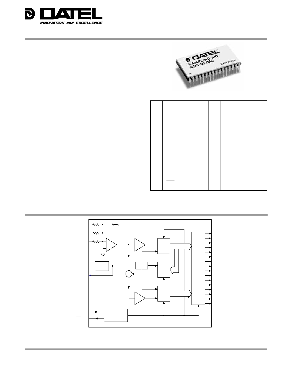
ADS-937
16-Bit, 1MHz, Low-Power
Sampling A/D Converters
GENERAL DESCRIPTION
The low-cost ADS-937 is a 16-bit, 1MHz sampling A/D con-
verter. This device accurately samples full-scale input signals
up to Nyquist frequencies with no missing codes. This feature,
combined with excellent signal-to-noise ratio (SNR) and total
harmonic distortion (THD), makes the ADS-937 the ideal
choice for both time-domain (CCD/medical imaging, scanners,
process control) and frequency-domain (radar, telecommunica-
tions, spectrum analysis) applications.
Packaged in a 32-pin, side-brazed, metal-sealed, ceramic
TDIP, the functionally complete ADS-937 contains a fast-
settling sample-hold amplifier, a subranging (two-pass) A/D
converter, an internal reference, timing/control logic, and error-
correction circuitry. Digital input and output levels are TTL.
ADS-937 only requires the rising edge of the start convert
pulse to operate.
Requiring Ī15V and Ī5V supplies, the ADS-937 typically
dissipates 1.25 Watts. The device is offered with both bipolar
(Ī5V) and unipolar (0 to ≠10V) analog input ranges. Models
are available for use in either commercial (0 to +70įC) or
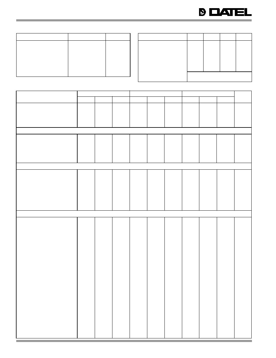
INPUT/OUTPUT CONNECTIONS
Figure 1. ADS-937 Functional Block Diagram
1
ANALOG INPUT
32
BIT 1 (MSB)
2
ANALOG GROUND
31
BIT 2
3
UNIPOLAR
30
BIT 3
4
OFFSET ADJUST
29
BIT 4
5
+5V REFERENCE OUT
28
BIT 5
6
GAIN ADJUST
27
BIT 6
7
COMPENSATION
26
BIT 7
8
≠15V SUPPLY
25
BIT 8
9
+15V SUPPLY
24
BIT 9
10
+5V ANALOG SUPPLY
23
BIT 10
11
≠5V ANALOG SUPPLY
22
BIT 11
12
ANALOG GROUND
21
BIT 12
13
DIGITAL GROUND
20
BIT 13
14
+5V DIGITAL SUPPLY
19
BIT 14
15
EOC
18
BIT 15
16
START CONVERT
17
BIT 16 (LSB)
PIN
FUNCTION
PIN
FUNCTION
REF
DAC
32 BIT 1 (MSB)
31 BIT 2
30 BIT 3
29 BIT 4
28 BIT 5
27 BIT 6
26 BIT 7
25 BIT 8
24 BIT 9
23 BIT 10
22 BIT 11
21 BIT 12
20 BIT 13
19 BIT 14
18 BIT 15
17 BIT 16 (LSB)
TIMING AND
CONTROL LOGIC
ANALOG INPUT 1
START CONVERT 16
EOC 15
≠
+
S/H
BUFFER
D
I
G
I
T
A
L
C
O
R
R
E
C
T
I
O
N
L
O
G
I
C
FLASH
ADC
1
FLASH
ADC
2
AMP
GAIN
CIRCUIT
COMPENSATION 7
+5V REFERENCE OUT 5
10
+5V ANALOG
SUPPLY
11
≠5V ANALOG
SUPPLY
2, 12
ANALOG
GROUND
14
+5V DIGITAL
SUPPLY
9
+15V
SUPPLY
8
≠15V
SUPPLY
13
DIGITAL
GROUND
OFFSET ADJUST 4
UNIPOLAR 3
GAIN ADJUST 6
DATEL, Inc., Mansfield, MA 02048 (USA)
∑
Tel: (508) 339-3000, (800) 233-2765 Fax: (508) 339-6356
∑
Email: sales@datel.com
∑
Internet:
www.datel.com
ģ
ģ
ADS-937
2
ģ
ģ
+25įC
0 to +70įC
≠55 to +125įC
ANALOG INPUTS
MIN.
TYP.
MAX.
MIN.
TYP.
MAX.
MIN.
TYP.
MAX.
UNITS
Input Voltage Ranges
Bipolar
--
Ī5
--
--
Ī5
--
--
Ī5
--
Volts
Unipolar
--
0 to ≠10
--
--
0 to ≠10
--
--
0 to ≠10
--
Volts
Input Resistance
--
1
--
--
1
--
--
1
--
k
Input Capacitance
--
7
15
--
7
15
--
7
15
pF
DIGITAL INPUTS
Logic Levels
Logic "1"
+2.0
--
--
+2.0
--
--
+2.0
--
--
Volts
Logic "0"
--
--
+0.8
--
--
+0.8
--
--
+0.8
Volts
Logic Loading "1"
--
--
+20
--
--
+20
--
--
+20
ĶA
Logic Loading "0"
--
--
≠20
--
--
≠20
--
--
≠20
ĶA
Start Convert Positive Pulse Width
20
500
--
20
500
--
20
500
--
ns
STATIC PERFORMANCE
Resolution
--
16
--
--
16
--
--
16
--
Bits
Integral Nonlinearity
--
Ī0.75
--
--
Ī1.5
--
--
Ī2
--
LSB
Differential Nonlinearity (f
in
= 10kHz)
≠0.95
Ī0.5
+1
≠ 0.95
Ī0.5
+1
≠0.95
Ī0.5
+1.5
LSB
Full Scale Absolute Accuracy
--
Ī0.1
Ī0.25
--
Ī0.2
Ī0.4
--
Ī0.25
Ī0.5
%FSR
Bipolar Zero Error (Tech Note 2)
--
Ī0.1
Ī0.15
--
Ī0.1
Ī0.25
--
Ī0.15
Ī0.5
%FSR
Bipolar Offset Error (Tech Note 2)
--
Ī0.1
Ī0.2
--
Ī0.15
Ī0.3
--
Ī0.2
Ī0.5
%FSR
Gain Error (Tech Note 2)
--
Ī0.1
Ī0.3
--
Ī0.25
Ī0.5
--
Ī0.4
Ī0.7
%
Unipolar Offset Error (Tech Note 2)
--
Ī0.1
Ī0.15
--
Ī0.1
Ī0.25
--
Ī0.15
Ī0.5
%FSR
No Missing Codes (f
in
= 10kHz)
16
--
--
16
--
--
16
--
--
Bits
DYNAMIC PERFORMANCE
Peak Harmonics (≠0.5dB)
dc to 100kHz
--
≠90
≠84
--
≠90
≠84
--
≠88
≠83
dB
100kHz to 500kHz
--
≠88
≠81
--
≠88
≠81
--
≠87
≠80
dB
Total Harmonic Distortion (≠0.5dB)
dc to 100kHz
--
≠87
≠82
--
≠87
≠82
--
≠86
≠81
dB
100kHz to 500kHz
--
≠86
≠81
--
≠86
≠81
--
≠85
≠80
dB
Signal-to-Noise Ratio
(w/o distortion, ≠0.5dB)
dc to 100kHz
85
88
--
85
88
--
84
87
--
dB
100kHz to 500kHz
84
87
--
84
87
--
83
87
--
dB
Signal-to-Noise Ratio
(& distortion, ≠0.5dB)
dc to 100kHz
81
85
--
81
85
--
80
84
--
dB
100kHz to 500kHz
80
84
--
80
84
--
78
83
--
dB
Noise
--
110
--
--
110
--
--
110
--
ĶVrms
Two-Tone Intermodulation
Distortion (f
in
= 100kHz,
240kHz, f
s
= 1MHz, ≠0.5dB)
--
≠85
--
--
≠85
--
--
≠85
--
dB
Input Bandwidth (≠3dB)
Small Signal (≠20dB input)
--
4.5
--
--
4.5
--
--
4.5
--
MHz
Large Signal (≠0.5dB input)
--
4
--
--
4
--
--
4
--
MHz
Feedthrough Rejection (f
in
= 500kHz)
--
84
--
--
84
--
--
84
--
dB
Slew Rate
--
Ī33
--
--
Ī33
--
--
Ī33
--
V/Ķs
Aperture Delay Time
--
+20
--
--
+20
--
--
+20
--
ns
Aperture Uncertainty
--
5
--
--
5
--
--
5
--
ps rms
S/H Acquisition Time
( to Ī0.003%FSR, 10V step)
--
260
300
--
260
300
--
260
300
ns
Overvoltage Recovery Time
--
500
1000
--
500
1000
--
500
1000
ns
A/D Conversion Rate
1
--
--
1
--
--
1
--
--
MHz
PARAMETERS
LIMITS
UNITS
+15V Supply (Pin 9)
0 to +16
Volts
≠15V Supply (Pin 8)
0 to ≠16
Volts
+5V Supply (Pins 10, 14)
0 to +6
Volts
≠5V Supply (Pin 11)
0 to ≠6
Volts
Digital Input (Pin 16)
≠0.3 to +V
DD
+0.3
Volts
Analog Input (Pin 1)
Ī15
Volts
Lead Temperature (10 seconds)
+300
įC
PARAMETERS
MIN.
TYP.
MAX.
UNITS
Operating Temp. Range, Case
ADS-937MC
0
--
+70
įC
ADS-937MM/883
≠55
--
+125
įC
Thermal Impedance
jc
--
5
--
įC/Watt
ca
--
22
--
įC/Watt
Storage Temperature Range
≠65
--
+150
įC
Package Type
32-pin,side-brazed, metal-sealed, ceramic TDIP
Weight
0.56 ounces (16 grams)
ABSOLUTE MAXIMUM RATINGS
PHYSICAL/ENVIRONMENTAL
FUNCTIONAL SPECIFICATIONS
(T
A
= +25įC, ĪV
CC
= Ī15V, ĪV
DD
= Ī5V, 1MHz sampling rate, and a minimum 1 minute warm-up unless otherwise specified.)
ADS-937
3
ģ
ģ
+25įC
0 to +70įC
≠55 to +125įC
ANALOG OUTPUT
MIN.
TYP.
MAX.
MIN.
TYP.
MAX.
MIN.
TYP.
MAX.
UNITS
Internal Reference
Voltage
+4.95
+5.0
+5.05
+4.95
+5.0
+5.05
+4.95
+5.0
+5.05
Volts
Drift
--
Ī30
--
--
Ī30
--
--
Ī30
--
ppm/įC
External Current
--
1
--
--
1
--
--
1
--
mA
DIGITAL OUTPUTS
Logic Levels
Logic "1"
+2.4
--
--
+2.4
--
--
+2.4
--
--
Volts
Logic "0"
--
--
+0.4
--
--
+0.4
--
--
+0.4
Volts
Logic Loading "1"
--
--
≠4
--
--
≠4
--
--
≠4
mA
Logic Loading "0"
--
--
+4
--
--
+4
--
--
+4
mA
Output Coding
Complementary Binary / Complementary Offset Binary
POWER REQUIREMENTS
Power Supply Ranges
+15V Supply
+14.5
+15.0
+15.5
+14.5
+15.0
+15.5
+14.5
+15.0
+15.5
Volts
≠15V Supply
≠14.5
≠15.0
≠15.5
≠14.5
≠15.0
≠15.5
≠14.5
≠15.0
≠15.5
Volts
+5V Supply
+4.75
+5.0
+5.25
+4.75
+5.0
+5.25
+4.75
+5.0
+5.25
Volts
≠5V Supply
≠4.75
≠5.0
≠5.25
≠4.75
≠5.0
≠5.25
≠4.75
≠5.0
≠5.25
Volts
Power Supply Currents
+15V Supply
--
+7
+9
--
+7
+9
--
+7
+9
mA
≠15V Supply
--
≠8
≠10
--
≠8
≠10
--
≠8
≠10
mA
+5V Supply
--
+133
+145
--
+133
+145
--
+133
+145
mA
≠5V Supply
--
≠72
≠80
--
≠72
≠80
--
≠72
≠80
mA
Power Dissipation
--
1.25
1.35
--
1.25
1.35
--
1.25
1.35
Watts
Power Supply Rejection
--
--
Ī0.01
--
--
Ī0.01
--
--
Ī0.01
%FSR/%V
THERMAL REQUIREMENTS
All DATEL sampling A/D converters are fully characterized and
specified over operating temperature (case) ranges of 0 to
+70įC and ≠55 to +125įC. All room-temperature (T
A
= +25įC)
production testing is performed without the use of heat sinks or
forced-air cooling. Thermal impedance figures for each device
are listed in their respective specification tables.
These devices do not normally require heat sinks, however,
standard precautionary design and layout procedures should be
used to ensure devices do not overheat. The ground and power
planes beneath the package, as well as all pcb signal runs to
and from the device, should be as heavy as possible to help
conduct heat away from the package. Electrically-insulating,
thermally-conductive "pads" may be installed underneath the
package. Devices should be soldered to boards rather than
"socketed", and of course, minimal air flow over the surface can
greatly help reduce the package temperature.
TECHNICAL NOTES
1. Obtaining fully specified performance from the ADS-937
requires careful attention to pc-card layout and power
supply decoupling. The device's analog and digital ground
systems are not connected to each other internally. For
optimal performance, tie all ground pins (2, 12 and 13)
directly to a large analog ground plane beneath the
package.
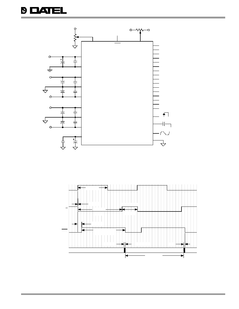
Bypass all power supplies and the +5V REFERENCE
OUTPUT (pin 5) to ground with 4.7ĶF tantalum capacitors in
parallel with 0.1ĶF ceramic capacitors. Locate the bypass
capacitors as close to the unit as possible. Tie a 47ĶF
capacitor between COMPENSATION (pin 7) and ground
(See figure 2.).
2. The ADS-937 achieves its specified accuracies without the
need for external calibration. If required, the device's small
initial offset and gain errors can be reduced to zero using
the adjustment circuitry shown in Figure 2. When using this
circuitry, or any similar offset and gain calibration hardware,
make adjustments following warm-up. To avoid interaction,
always adjust offset before gain. Float pins 4 and 6 if not
using offset and gain adjust circuits.
Footnotes:
This is the time required before the A/D output data is valid once the analog input
is back within the specified range.
6.02
(SNR + Distortion) ≠ 1.76 + 20 log
Full Scale Amplitude
Actual Input Amplitude
All power supplies must be on before applying a start convert pulse. All
supplies and the clock (START CONVERT) must be present during warm-up
periods. The device must be continuously converting during this time.
Contact DATEL for other input voltage ranges.
A 1MHz clock with a 500nsec positive pulse width (50% duty cycle) is used for
all production testing. Any duty cycle may be used as long as a minimum
positive pulse width of 20nsec is maintained. For applications requiring lower
sampling rates, clock frequencies less than 1MHz may be used.
Effective bits is equal to:
3. Applying a start convert pulse while a conversion is in
progress (EOC = logic "1") will initiate a new and inaccurate
conversion cycle. Data for the interrupted and subsequent
conversions will be invalid.
ADS-937
4
ģ
ģ
3. For a bipolar input - Adjust the offset potentiometer until the
output code flickers equally between 1000 0000 0000 0000
and 0111 1111 1111 1111.
For a unipolar input - Adjust the offset potentiometer until
all output bits are 0's and the LSB flickers between 0 and 1.
Gain Adjust Procedure
1. Apply ≠4.999771V to the ANALOG INPUT (pin 1) for
bipolar gain adjust or apply ≠9.999771V to pin 1 for
unipolar gain adjust.
2. For a unipolar input - Adjust the gain potentiometer until all
output bits are 1's and the LSB flickers between 1 and 0.
For a bipolar input - Adjust the gain potentiometer until all
output bits are 1's and the LSB flickers between 1 and 0.
3. To confirm proper operation of the device, vary the applied
input voltage to obtain the output coding listed in Table 2.
UNIPOLAR
INPUT VOLTAGE
INPUT RANGE
BIPOLAR
SCALE
0 to ≠10V
MSB
LSB
MSB
LSB
Ī5V
SCALE
≠FS +1 LSB
≠9.999847
1111 1111 1111 1111
0000 0000 0000 0000
+4.999847
+FS ≠1 LSB
≠7/8 FS
≠8.750000
1110 0000 0000 0000
0001 1111 1111 1111
+3.750000
+3/4 FS
≠3/4 FS
≠7.500000
1100 0000 0000 0000
0011 1111 1111 1111
+2.500000
+1/2 FS
≠1/2 FS
≠5.000000
1000 0000 0000 0000
0111 1111 1111 1111
+0.000000
0
≠1/4 FS
≠2.500000
0100 0000 0000 0000
1011 1111 1111 1111
≠2.500000
≠1/2 FS
≠1/8 FS
≠1.250000
0010 0000 0000 0000
1101 1111 1111 1111
≠3.750000
≠3/4 FS
≠1 LSB
≠0.000153
0000 0000 0000 0001
1111 1111 1111 1110
≠4.999847
≠FS +1 LSB
0
0.000000
0000 0000 0000 0000
1111 1111 1111 1111
≠5.000000
≠FS
OUTPUT CODING
COMPLEMENTARY
BINARY
COMPLEMENTARY
OFFSET BINARY
Table 2. Output Coding
CALIBRATION PROCEDURE
Connect the converter per Table 1 for the appropriate input
voltage range. Any offset/gain calibration procedures should
not be implemented until the device is fully warmed up. To
avoid interaction, adjust offset before gain. The ranges of
adjustment for the circuits in Figure 2 are guaranteed to
compensate for the ADS-937's initial accuracy errors and may
not be able to compensate for additional system errors.
A/D converters are calibrated by positioning their digital
outputs exactly on the transition point between two adjacent
digital output codes. This is accomplished by connecting
LED's to the digital outputs and performing adjustments until
certain LED's "flicker" equally between on and off. Other
approaches employ digital comparators or microcontrollers to
detect when the outputs change from one code to the next.
For the ADS-937, offset adjusting is normally accomplished
when the analog input is 0 minus ĹLSB (≠76.3ĶV). See Table
2 for the proper bipolar and unipolar output coding.
Gain adjusting is accomplished when the analog input is at
nominal full scale minus 1ĹLSB's (≠9.999771V for unipolar
and ≠4.999771V for bipolar).
Zero/Offset Adjust Procedure
1. Apply a train of pulses to the START CONVERT input
(pin 16) so that the converter is continuously converting.
2. For unipolar or bipolar zero/offset adjust, apply ≠76.3ĶV to
the ANALOG INPUT (pin 1).
INPUT VOLTAGE
INPUT
TIE
RANGE
PIN
TOGETHER
Ī5V
Pin 1
Pins 2 and 3
0 to ≠10V
Pin 1
Pins 3 and 5
Table 1. Input Connections
ADS-937
5
ģ
ģ
Figure 3. ADS-937 Timing Diagram
Figure 2. Typical ADS-937 Connection Diagram
Scale is approximately 50ns per division.
START
CONVERT
INTERNAL S/H
N
N+1
500ns typ.
Acquisition Time
260ns typ.
740ns typ.
5ns typ.
EOC
65ns typ.
Conversion Time
730ns typ.
OUTPUT
DATA
Data N-2 Valid
980ns typ.
Hold
Data N-1 Valid
20ns typ.
20ns
Invalid Data
N
Note: Scale is approximately 50ns per division. Sampling Rate = 1MHz.
2
11
ADS-937
20k
10
32
31
30
29
28
27
26
25
24
23
22
21
20
19
18
17
BIT 1 (MSB)
BIT 2
BIT 3
BIT 4
BIT 5
BIT 6
BIT 7
BIT 8
BIT 9
BIT 10
BIT 11
BIT 12
BIT 13
BIT 14
BIT 15
BIT 16 (LSB)
+5V ANALOG
15
ANALOG
GROUND
ANALOG
GROUND
DIGITAL
GROUND
0.1ĶF
4.7ĶF
0.1ĶF
UNIPOLAR
+
4.7ĶF
+5V
REF. OUT
COMPENSATION
47ĶF
14
13
3
5
7
START CONVERT
+5V DIGITAL
≠15V
+15V
OFFSET
ADJUST
GAIN
ADJUST
4
6
16
0.1ĶF
4.7ĶF
12
9
0.1ĶF
4.7ĶF
8
+
+
0.1ĶF
4.7ĶF
0.1ĶF
4.7ĶF
+
+
EOC
≠5V ANALOG
+15V
≠15V
ANALOG INPUT
1
Pin 5 (ADS-937)
10k