 | –≠–ª–µ–∫—Ç—Ä–æ–Ω–Ω—ã–π –∫–æ–º–ø–æ–Ω–µ–Ω—Ç: ADS-944MC | –°–∫–∞—á–∞—Ç—å:  PDF PDF  ZIP ZIP |
1
+5V ANALOG SUPPLY
32
START CONVERT
2
≠5.2V DIGITAL SUPPLY
31
BIT 1 (MSB)
3
ANALOG INPUT
30
BIT 1 (MSB)
4
ANALOG GROUND
29
BIT 2
5
OFFSET ADJUST
28
BIT 3
6
ANALOG GROUND
27
BIT 4
7
GAIN ADJUST
26
BIT 5
8
COMP. BITS
25
BIT 6
9
OUTPUT ENABLE
24
BIT 7
10
+5V DIGITAL SUPPLY
23
BIT 8
11
ANALOG GROUND
22
BIT 9
12
+15V SUPPLY
21
BIT 10
13
≠15V SUPPLY
20
BIT 11
14
≠5.2V ANALOG SUPPLY
19
BIT 12
15
DIGITAL GROUND
18
BIT 13
16
EOC
17
BIT 14 (LSB)
FEATURES
∑
14-bit resolution
∑
5MHz minimum sampling rate
∑
No missing codes over full military temperature range
∑
Edge-triggered, no pipeline delay
∑
Low power, 2.95 Watts
∑
Small, 32-pin, ceramic TDIP package
∑
SMT package available
∑
Excellent dynamic performance
∑
MIL-STD-883 screening or DESC SMD available
Æ
Æ
ADS-944
14-Bit, 5MHz
Sampling A/D Converters
DATEL, Inc., 11 Cabot Boulevard, Mansfield, MA 02048-1151 (U.S.A.)
∑
Tel: (508) 339-3000 Fax: (508) 339-6356
∑
For immediate assistance: (800) 233-2765
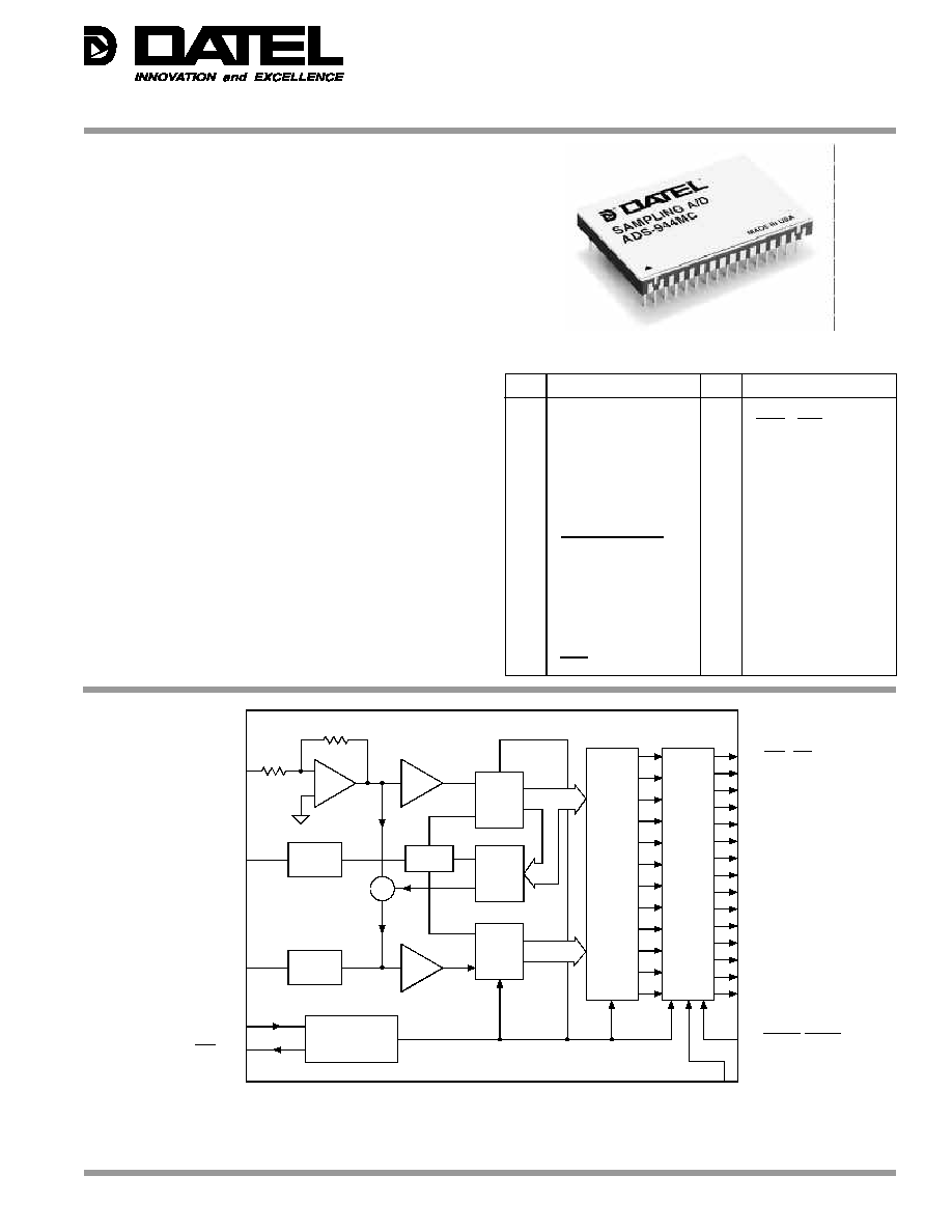
GENERAL DESCRIPTION
The low-cost ADS-944 is a high-performance, 14-bit, 5MHz
sampling A/D converter. This device accurately samples full-
scale input signals up to Nyquist frequencies with no missing
codes. The dynamic performance of the ADS-944 has been
optimized to achieve a THD of ≠77dB and a SNR of 76dB.
Packaged in a small, 32-pin TDIP, the functionally complete
ADS-944 contains a fast-settling sample-hold amplifier, a
subranging (two-pass) A/D converter, an internal reference,
timing and control logic, three-state outputs, and error-
correction circuitry. Digital input and output levels are TTL.
Requiring ±15V, +5V and ≠5.2V supplies, the ADS-944
typically dissipates 2.95 Watts. The unit is offered with a
bipolar input range of ±1.25V. Models are available for use in
either commercial (0 to +70∞C) or military (≠55 to +125∞C)
operating temperature ranges. Typical applications include
radar signal analysis, medical/graphic imaging, and
FFT spectrum analysis.
INPUT/OUTPUT CONNECTIONS
PIN
FUNCTION
PIN
FUNCTION
Figure 1. ADS-944 Functional Block Diagram
REF
DAC
3
-
S
T
A
T
E
O
U
T
P
U
T
R
E
G
I
S
T
E
R
31 BIT 1 (MSB)
30 BIT 1 (MSB)
29 BIT 2
28 BIT 3
27 BIT 4
26 BIT 5
25 BIT 6
24 BIT 7
23 BIT 8
22 BIT 9
21 BIT 10
20 BIT 11
19 BIT 12
18 BIT 13
17 BIT 14 (LSB)
TIMING AND
CONTROL LOGIC
ANALOG INPUT 3
START CONVERT 32
EOC 16
≠
+
S/H
BUFFER
D
I
G
I
T
A
L
C
O
R
R
E
C
T
I
O
N
L
O
G
I
C
FLASH
ADC
1
FLASH
ADC
2
AMP
GAIN
CIRCUIT
GAIN ADJUST 7
OFFSET
CIRCUIT
OFFSET ADJUST 5
1
+5V
ANALOG
SUPPLY
2
≠5.2V
DIGITAL
SUPPLY
4, 6, 11
ANALOG
GROUND
10
+5V
DIGITAL
SUPPLY
12
+15V
SUPPLY
14
≠5.2V
ANALOG
SUPPLY
15
DIGITAL
GROUND
8
COMP.
BITS
9 OUTPUT ENABLE
ADS-944
2
Æ
Æ
PARAMETERS
LIMITS
UNITS
+15V Supply (Pins 12)
0 to +16
Volts
≠15V Supply (Pin 13)
0 to ≠16
Volts
+5V Supply (Pins 1, 10)
0 to +6
Volts
≠5V Supply (Pin 2, 14)
0 to ≠6
Volts
Digital Input (Pin 8, 9, 32)
≠0.3 to +V
DD
+0.3
Volts
Analog Input (Pin 3)
≠5 to +5
Volts
Lead Temperature (10 seconds)
+300
∞C
PARAMETERS
MIN.
TYP.
MAX.
UNITS
Operating Temp. Range, Case
ADS-944MC
0
--
+70
∞C
ADS-944MM/883
≠55
--
+125
∞C
Thermal Impedance
jc
--
7
--
∞C/Watt
ca
--
21
--
∞C/Watt
Storage Temperature Range
≠65
--
+150
∞C
Package Type
32-pin, metal-sealed, ceramic TDIP or SMT
Weight
0.46 ounces (13 grams)
ABSOLUTE MAXIMUM RATINGS
PHYSICAL/ENVIRONMENTAL
FUNCTIONAL SPECIFICATIONS
(T
A
= +25∞C, ±V
CC
= ±15V, +V
DD
= +5V,V
dd
= ≠5.2V, 5MHz sampling rate, and a minimum 3 minute warmup unless otherwise specified.)
+25∞C
0 to +70∞C
≠55 to +125∞C
ANALOG INPUT
MIN.
TYP.
MAX.
MIN.
TYP.
MAX.
MIN.
TYP.
MAX.
UNITS
Input Voltage Range
--
±1.25
--
--
±1.25
--
--
±1.25
--
Volts
Input Resistance
500
550
--
500
550
--
500
550
--
Input Capacitance
--
6
15
--
6
15
--
6
15
pF
DIGITAL INPUT
Logic Levels
Logic "1"
+2.0
--
--
+2.0
--
--
+2.0
--
--
Volts
Logic "0"
--
--
+0.8
--
--
+0.8
--
--
+0.8
Volts
Logic Loading "1"
--
--
+20
--
--
+20
--
--
+20
µA
Logic Loading "0"
--
--
≠20
--
--
≠20
--
--
≠20
µA
Start Convert Positive Pulse Width
40
80
--
40
80
--
40
80
--
ns
STATIC PERFORMANCE
Resolution
--
14
--
--
14
--
--
14
--
Bits
Integral Nonlinearity (f
in
= 10kHz)
--
±0.75
--
--
±0.75
--
--
±1.0
--
LSB
Differential Nonlinearity (f
in
= 10kHz)
≠0.95
±0.5
+1.2
≠0.95
±0.5
+1.2
≠0.95
±0.5
+1.5
LSB
Full Scale Absolute Accuracy
--
±0.15
±0.4
--
±0.15
±0.4
--
±0.4
±0.8
%FSR
Bipolar Zero Error (Tech Note 2)
--
±0.1
±0.3
--
±0.1
±0.3
--
±0.3
±0.6
%FSR
Bipolar Offset Error (Tech Note 2)
--
±0.2
±0.4
--
±0.2
±0.4
--
±0.3
±0.9
%FSR
Gain Error (Tech Note 2)
--
±0.2
±0.4
--
±0.2
±0.4
--
±0.4
±1.5
%
No Missing Codes (f
in
= 10kHz)
14
--
--
14
--
--
14
--
--
Bits
DYNAMIC PERFORMANCE
Peak Harmonics (≠0.5dB)
dc to 100kHz
--
≠85
≠77
--
≠85
≠75
--
≠81
≠71
dB
100kHz to 1MHz
--
≠78
≠71
--
≠78
≠70
--
≠75
≠67
dB
1MHz to 2.5MHz
--
≠75
≠70
--
≠75
≠68
--
≠71
≠61
dB
Total Harmonic Distortion (≠0.5dB)
dc to 100kHz
--
≠82
≠76
--
≠82
≠74
--
≠78
≠70
dB
100kHz to 1MHz
--
≠77
≠70
--
≠77
≠70
--
≠73
≠65
dB
1MHz to 2.5MHz
--
≠73
≠68
--
≠73
≠65
--
≠70
≠60
dB
Signal-to-Noise Ratio
(w/o distortion, ≠0.5dB)
dc to 100kHz
73
76
--
73
76
--
71
75
--
dB
100kHz to 1MHz
73
76
--
73
76
--
71
75
--
dB
1MHz to 2.5MHz
73
75
--
73
75
--
71
75
--
dB
Signal-to-Noise Ratio
(& distortion, ≠0.5dB)
dc to 100kHz
71
75
--
71
75
--
68
73
--
dB
100kHz to 1MHz
70
73
--
69
73
--
65
71
--
dB
1MHz to 2.5MHz
68
71
--
66
71
--
62
69
--
dB
Noise
--
135
--
--
135
--
--
135
--
µVrms
Two-tone Intermodulation
Distortion (f
in
= 2.45MHz,
1.975MHz, f
s
= 5MHz, ≠0.5dB)
--
≠82
--
--
≠82
--
--
≠82
--
dB
Input Bandwidth (≠3dB)
Small Signal (≠20dB input)
--
20
--
--
20
--
--
20
--
MHz
Large Signal (≠0.5dB input)
--
13
--
--
13
--
--
13
--
MHz
Feedthrough Rejection (f
in
= 2.5MHz)
--
90
--
--
90
--
--
90
--
dB
Slew Rate
--
±110
--
--
±110
--
--
±110
--
V/µs
Aperture Delay Time
--
+10
--
--
+10
--
--
+10
--
ns
Aperture Uncertainty
--
3
--
--
3
--
--
3
--
ps rms

ADS-944
3
Æ
Æ
+25∞C
0 to +70∞C
≠55 to +125∞C
DYNAMIC PERFORMANCE cont.
MIN.
TYP.
MAX.
MIN.
TYP.
MAX.
MIN.
TYP.
MAX.
UNITS
S/H Acquisition Time
( to ±0.003%FSR, 2.5V step)
--
85
90
--
85
90
--
85
90
ns
Overvoltage Recovery Time
--
200
--
--
200
--
--
200
--
ns
A/D Conversion Rate
5
--
--
5
--
--
5
--
--
MHz
DIGITAL OUTPUTS
Logic Levels
Logic "1"
+2.4
--
--
+2.4
--
--
+2.4
--
--
Volts
Logic "0"
--
--
+0.4
--
--
+0.4
--
--
+0.4
Volts
Logic Loading "1"
--
--
≠4
--
--
≠4
--
--
≠4
mA
Logic Loading "0"
--
--
+4
--
--
+4
--
--
+4
mA
Delay, Edge of ENABLE
to Output Data Valid/Invalid
--
--
10
--
--
10
--
--
10
ns
Output Coding
Offset Binary, Complementary Offset Binary, Two's Complement
POWER REQUIREMENTS
Power Supply Ranges
+15V Supply
+14.25
+15.0
+15.75
+14.25
+15.0
+15.75
+14.25
+15.0
+15.75
Volts
≠15V Supply
≠14.25
≠15.0
≠15.75
≠14.25
≠15.0
≠15.75
≠14.25
≠15.0
≠15.75
Volts
+5V Supply
+4.75
+5.0
+5.25
+4.75
+5.0
+5.25
+4.9
+5.0
+5.25
Volts
≠5V Supply
≠4.95
≠5.2
≠5.45
≠4.95
≠5.2
≠5.45
≠5.1
≠5.2
≠5.45
Volts
Power Supply Currents
+15V Supply
--
+36
+45
--
+36
+45
--
+36
+45
mA
≠15V Supply
--
≠55
≠65
--
≠55
≠65
--
≠55
≠65
mA
+5V Supply
--
+155
+168
--
+155
+168
--
+155
+168
mA
≠5.2V Supply
--
≠167
≠175
--
≠167
≠175
--
≠167
≠175
mA
Power Dissipation
--
2.95
3.3
--
2.95
3.3
--
2.95
3.3
Watts
Power Supply Rejection
--
--
±0.05
--
--
±0.05
--
--
±0.05
%FSR/%V
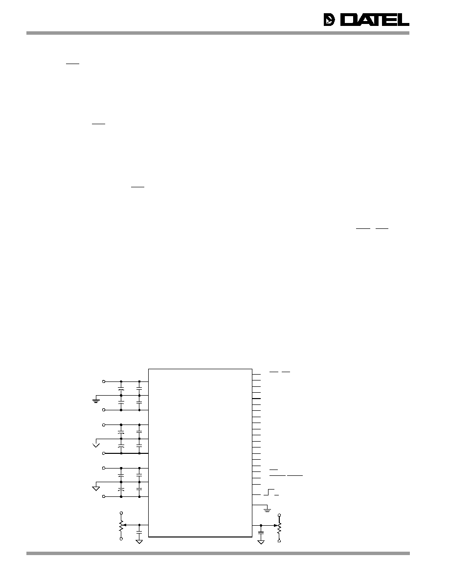
TECHNICAL NOTES
1. Obtaining fully specified performance from the ADS-944
requires careful attention to pc-card layout and power
supply decoupling. The device's analog and digital ground
systems are not connected to each other internally. For
optimal performance, tie all ground pins (4, 6, 11, and 15)
directly to a large analog ground plane beneath the
package. Bypass all power supplies to ground with 4.7µF
tantalum capacitors in parallel with 0.1µF ceramic capaci-
tors. It is very important that the bypass capacitors be
located as close to the unit as possible. Inductors or
ferrite beads can also be used to improve the power supply
filtering. Refer to Figure 4, the ADS-944 Evaluation Board
Schematic, for more details.
2. The ADS-944 achieves its specified accuracies without the
need for external calibration. If required, the device's small
initial offset and gain errors can be reduced to zero using
the adjustment circuitry shown in Figure 2. When using this
circuitry, or any similar offset and gain-calibration hardware,
make adjustments following warmup. To avoid interaction,
always adjust offset before gain.
3. Pin 8 (COMP. BITS) selects the ADS-944's digital output
coding. When a logic "1" is applied to pin 8, the output
coding is complementary offset binary. When pin 8 has a
logic "0" applied, the output coding becomes offset binary.
The MSB output (pin 31) may be used under these condi-
tions to achieve two's complement coding. Pin 8 is TTL-
compatible and can be driven with digital logic for those who
want dynamic control of its function. There is an internal
pull-up resistor on this pin, allowing pin 8 to be either
connected to +5V or left open when a logic "1" is needed.
4. To enable the three-state outputs, apply a logic "0" (low) to
OUTPUT ENABLE (pin 9). To disable, apply a logic "1"
(high) to pin 9.
Footnotes:
All power supplies should be on before applying a start convert pulse. All
supplies and the clock (start convert pulses) must be present during warmup
periods. The device must be continuously converting during this time.
When COMP. BITS (pin 8) is low, logic loading "0" will be ≠350µA for this pin.
An 80ns wide start convert pulse is used for all production testing. The start
convert pulse should be between 40 ≠ 80ns or 130 ≠ 160ns to ensure proper
operations. The latter range could be used for those applications requiring less
than a 5MHz sampling rate.
6.02
(SNR + Distortion) ≠ 1.76 + 20 log
Full Scale Amplitude
Actual Input Amplitude
Effective bits is equal to:
This is the time required before the A/D output is valid after the analog input is
back within its range.
The minimum supply voltages of +4.9V and ≠5.1V for ±V
DD
are required for
≠55∞C operations only. The minimum limits are +4.75V and ≠4.95V when
operating at +125∞C.
Typical +5V and ≠5.2V current drain breakdowns are as follows:
+5V
Analog
= +85mA
≠5.2V
Analog
= ≠114mA
+5V
Digital
= +70mA
≠5.2V
Digital
= ≠53mA
+5V
Total
= +155mA
≠5.2V
Total
= ≠167mA
ADS-944
4
Æ
Æ
For the ADS-944, offset adjusting is normally accomplished at
the point where the MSB is a 1 and all other output bits are 0's
and the LSB just changes from a 0 to a 1. This digital output
transition ideally occurs when the applied analog input is
+Ω LSB (+76.3µV).
Gain adjusting is accomplished when all bits are 1's and the
LSB just changes from a 1 to a 0. This transition ideally
occurs when the analog input is at +full scale minus 1Ω LSB's
(+1.249771) .
Note: Due to inherent system noise, the averaging of several
conversions may be needed to accurately adjust both offset
and gain to 1LSB of accuracy.
Zero/Offset Adjust Procedure
1. Apply a train of pulses to the START CONVERT input
(pin 32) so the converter is continuously converting.
2. Apply +76.3µV to the ANALOG INPUT (pin 3).
3. Adjust the offset potentiometer until the output bits are
10 0000 0000 0000 and the LSB flickers between 0 and 1
with pin 8 tied low (offset binary) or between 01 1111 1111
1111 and 01 1111 1111 1110 with pin 8 tied high
(complementary offset binary).
4. Two's complement coding requires using BIT 1 (MSB)
(pin 31). With pin 8 tied low, adjust the trimpot until the
code flickers between 00 0000 0000 0000 and 00 0000
0000 0001.
Gain Adjust Procedure
1. Apply +1.249771V to the ANALOG INPUT (pin 3).
2. Adjust the gain potentiometer until all output bits are 1's and
the LSB flickers between 1 and 0 with pin 8 tied low (offset
binary) or until all bits are 0's and the LSB flickers between
1 and 0 with pin 8 tied high (complementary offset binary).
3. Two's complement coding requires using pin 31. With pin 8
tied low, adjust the gain trimpot until the output code flickers
equally between 01 1111 1111 1110 and 01 1111 1111 1111.
4. To confirm proper operation of the device, vary the applied
input voltage to obtain the output coding listed in Table 1.
TECHNICAL NOTES CONT.
5. Applying a start convert pulse while a conversion is in
progress (EOC = logic "1") initiates a new and inaccurate
conversion cycle. Data for the interrupted and subsequent
conversions will be invalid.
6. A passive bandpass filter is used at the input of the A/D for
all production testing.
7. Though the ADS-944's digital outputs are capable of
driving multiple LSTTL or HCT loads, we recommend the
output bits and the EOC line each drive only a single gate.
These gates should be located as close to the unit as
possible. If they can not, 33
resistors placed in series
with each output can aid in isolating pc run inductances.
The ADS-944 digital outputs should not be connected
directly to noisy digital busses.
8. Do not enable/disable or complement the output bits during
the conversion process (from the falling edge of START
CONVERT to the falling edge of EOC).
CALIBRATION PROCEDURE
(Refer to Figure 2 and Table 1)
Note: Connect pin 5 to ANALOG GROUND (pin 6) for
operation without zero/offset adjustment. Connect pin 7 to
ANALOG GROUND (pin 6) for operation without gain
adjustment.
Any offset and/or gain calibration procedures should not be
implemented until devices are fully warmed up. To avoid
interaction, offset must be adjusted before gain. The ranges of
adjustment for the circuit in Figure 2 are guaranteed to
compensate for the ADS-944's initial accuracy errors and may
not be able to compensate for additional system errors.
A/D converters are calibrated by positioning their digital
outputs exactly on the transition point between two adjacent
digital output codes. This can be accomplished by connecting
LED's to the digital outputs and adjusting until certain LED's
"flicker" equally between on and off. Other approaches
employ digital comparators or microcontrollers to detect when
the outputs change from one code to the next.
Figure 2. ADS-944
Connection Diagram
ADS-944
20k
31
30
29
28
27
26
25
24
23
22
21
20
19
18
17
7
16
9
3
BIT 1 (MSB)
BIT 1 (MSB)
BIT 2
BIT 3
BIT 4
BIT 5
BIT 6
BIT 7
BIT 8
BIT 9
BIT 10
BIT 11
BIT 12
BIT 13
BIT 14 (LSB)
OVERFLOW
EOC
OUTPUT ENABLE
ANALOG INPUT
ANALOG
SUPPLY
DIGITAL
SUPPLY
10
15
OFFSET
ADJUST
5
0.1µF
4.7µF
4, 6
14
0.1µF
4.7µF
1
+
+
≠5.2V
+5V
32
START CONVERT
2
COMP. BITS
0.1µF
4.7µF
0.1µF
4.7µF
+
+
≠5.2V
+5V
2
0.1µF
4.7µF
11
13
0.1µF
4.7µF
12
+
+
≠15V
+15V
DIGITAL
SUPPLY
ANALOG
SUPPLY
0.1µF
7
GAIN
ADJUST
20k
≠15V
+15V
≠15V
+15V
ADS-944
5
Æ
Æ
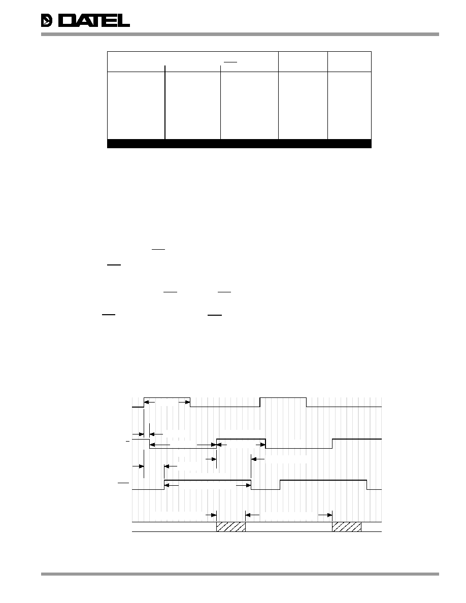
TIMING
The ADS-944 is an edge-triggered device. A conversion is
initiated by the rising edge of the start convert pulse and no
additional external timing signals are required. The device
does not employ "pipeline" delays to increase its throughput
rate. It does not require multiple start convert pulses to bring
valid digital data to its output pins.
Approximately 10ns after the rising edge of the start convert
signal, the ADS-944's internal sample-hold amplifier is driven
into the hold mode by the internal S/H control line. After a
35ns delay to allow for S/H output transient settling, the
conversion process begins, and the EOC line (pin 16) is driven
high. The complete A/D conversion requires approximately
150ns. The falling of EOC signals that the conversion is now
complete and digital output data is now valid.
This device actually guarantees that digital output data will be
valid for 10ns prior to the falling edge of EOC. Therefore, EOC
can be used to latch data into external registers that have
appropriate setup times. Any other available timing edges,
including a delayed EOC or the rising edge of the next EOC
pulse, can also be used for this purpose.
The falling edge of the start convert pulse, though irrelevant to
device timing, can cause conversion errors if it occurs at
certain times. Therefore, the recommended start convert
pulse width is between 40 and 80ns or between 130 and
160ns. DATEL performs ADS-944 production testing at the full
5MHz sampling rate using 80ns start convert pulses.
Table 1. Output Coding
OUTPUT CODING
INPUT RANGE
BIPOLAR
MSB
LSB
MSB
LSB
MSB
LSB
±1.25V
SCALE
OFF. BINARY
COMP. OFF. BIN.
TWO'S COMP.
11 1111 1111 1111
00 0000 0000 0000 01 1111 1111 1111
+1.249847
+FS ≠1 LSB
11 1000 0000 0000
00 1111 1111 1111
01 1000 0000 0000
+0.937500
+3/4 FS
11 0000 0000 0000
00 1111 1111 1111
01 0000 0000 0000
+0.625000
+1/2FS
10 0000 0000 0000 01 1111 1111 1111
00 0000 0000 0000
0.000000
0
01 0000 0000 0000 10 1111 1111 1111
11 0000 0000 0000
≠0.625000
≠1/2FS
00 1000 0000 0000 11 0111 1111 1111
10 1000 0000 0000
≠0.937500
≠3/4FS
00 0000 0000 0001 11 1111 1111 1110
10 0000 0000 0001
≠1.249847
≠FS +1 LSB
00 0000 0000 0000 11 1111 1111 1111
10 0000 0000 0000
≠1.250000
≠FS
Figure 3. ADS-944 Timing Diagram
THERMAL REQUIREMENTS
All DATEL sampling A/D converters are fully characterized and
specified over operating temperature (case) ranges of 0 to
+70∞C and ≠55 to +125∞C. All room-temperature (T
A
= +25∞C)
production testing is performed without the use of heat sinks or
forced-air cooling. Thermal impedance figures for each device
are listed in their respective specification tables.
These devices do not normally require heat sinks, however,
standard precautionary design and layout procedures should
be used to ensure devices do not overheat. The ground and
power planes beneath the package, as well as all pcb signal
runs to and from the device, should be as heavy as possible to
help conduct heat away from the package.
Electrically-insulating, thermally-conductive "pads" may be
installed underneath the package. Devices should be
soldered to boards rather than "socketed", and of course,
minimal air flow over the surface can greatly help reduce the
package temperature.
In more severe ambient conditions, the package/junction
temperature of a given device can be reduced dramatically
(typically 35%) by using one of DATEL's HS Series heat sinks.
See Ordering Information for the assigned part number. See
page 1-183 of the DATEL Data Acquisition Components
Catalog for more information on the HS Series. Request
DATEL Application Note AN-8, "Heat Sinks for DIP Data
Converters", or contact DATEL directly, for additional
information.
START
CONVERT
OUTPUT
DATA
INTERNAL S/H
N
N+1
DATA (N-1) VALID
Acquisition Time
10ns typ.
DATA N VALID
Note: Scale is approximately 10ns per division.
EOC
Conversion Time
INVALID
DATA
35ns typ.
Hold
80ns typ.
115ns typ.
150ns typ., 160ns max.
60ns typ., ±10ns
Hold
140ns min., 150ns typ.
START CONVERT pulse width: 40 to 80ns or 130 to 160ns.
50ns typ., 60ns max.
90ns max.