 | –≠–ª–µ–∫—Ç—Ä–æ–Ω–Ω—ã–π –∫–æ–º–ø–æ–Ω–µ–Ω—Ç: ADS-945EX | –°–∫–∞—á–∞—Ç—å:  PDF PDF  ZIP ZIP |
Æ
Æ
ADS-945
14-Bit, 10MHz
Sampling A/D Converters
DATEL, Inc., 11 Cabot Boulevard, Mansfield, MA 02048-1151 (U.S.A.)
∑
Tel: (508) 339-3000 Fax: (508) 339-6356
∑
For immediate assistance: (800) 233-2765
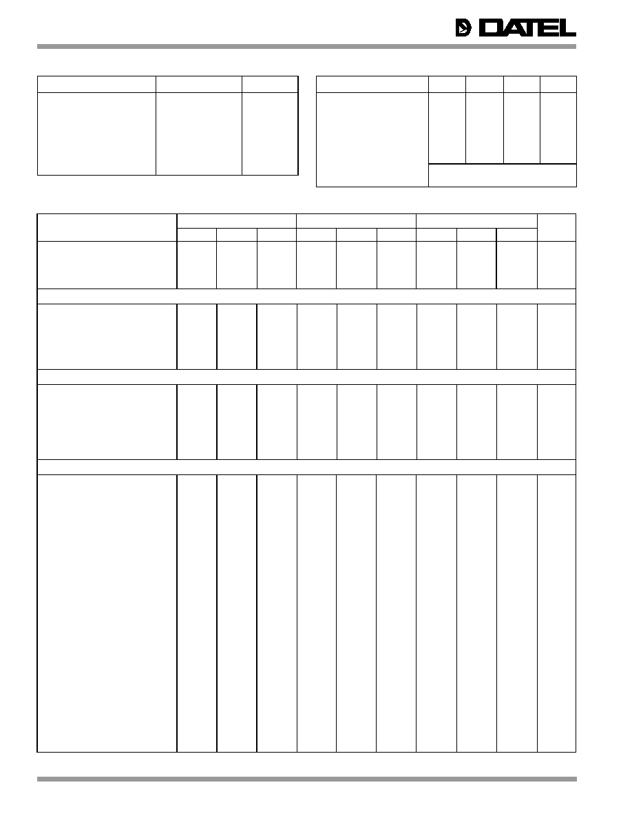
Figure 1. ADS-945 Functional Block Diagram
FEATURES
∑
14-bit resolution
∑
10MHz minimum throughput
∑
Functionally complete
∑
No missing codes
∑
Low power, 4.2W
∑
Excellent dynamic performance
∑
Internally clamped input
∑
Edge triggered
∑
TTL compatible
∑
2" x 4" module
∑
Very low profile
GENERAL DESCRIPTION
The low-cost ADS-945 is a high-performance, 14-bit, 10MHz
sampling A/D converter. This device accurately samples
full-scale input signals up to Nyquist frequencies with no
missing codes. The dynamic performance of the ADS-945
has been optimized to achieve a THD of ≠82dB and a
SNR of 79dB.
Packaged in a 2" x 4" module, the functionally complete
ADS-945 contains a fast-settling sample/hold amplifier, a
subranging (two-pass) A/D converter, a precise voltage
reference, timing/control logic, three-state outputs, and
error-correction circuitry. Digital inputs and outputs are TTL
compatible (except for pins 29 and 30 which are ECL).
Requiring ±15V, +5V and ≠5.2V supplies, the ADS-945
typically dissipates 4.2W. The unit is offered with a bipolar
input range of ±1.25V. Models are available for use in either
commercial (0 to +70∞C) or military (≠55 to +125∞C) operating
temperature ranges. Typical applications include radar signal
analysis, medical/graphic imaging, and FFT spectrum
analysis.
1
ANALOG GROUND
70-76
ANALOG GROUND
4
ANALOG INPUT
69
+5V ANALOG SUPPLY
5-6
ANALOG GROUND
64-68
ANALOG GROUND
7
+10V REFERENCE OUT
63
≠5.2V ANALOG SUPPLY
8
ANALOG GROUND
62
ANALOG GROUND
9
GAIN ADJUST
61
NO CONNECT
10-11
DO NOT CONNECT
58-60
DIGITAL GROUND
12
≠15V SUPPLY
57
≠5.2V DIGITAL SUPPLY
13
ANALOG GROUND
56
DO NOT CONNECT
14
+15V SUPPLY
55
+5V DIGITAL SUPPLY
15-17
ANALOG GROUND
54
DIGITAL GROUND
18
OFFSET ADJUST
53
BIT 1 (MSB)
19-25
ANALOG GROUND
52
BIT 2
26
MISSING PIN
51
BIT 3
27
DIGITAL GROUND
50
BIT 4
28
DIGITAL GROUND
49
BIT 5
29
T/H STATUS
48
BIT 6
30
T/H STATUS
47
BIT 7
31
DIGITAL GROUND
46
BIT 8
32
START CONVERT
45
BIT 9
33
OVERFLOW
44
BIT 10
34
OUTPUT ENABLE (OE)
43
BIT 11
35
DIGITAL GROUND
42
BIT 12
36
O.S. 3 *
41
BIT 13
37
DIGITAL GROUND
40
BIT 14 (LSB)
38
DIGITAL GROUND
39
DIGITAL GROUND
INPUT/OUTPUT CONNECTIONS
PIN
FUNCTION
PIN
FUNCTION
* Refer to Timing Diagram notes
REF
DAC
3
-
S
T
A
T
E
O
U
T
P
U
T
R
E
G
I
S
T
E
R
53
52
51
50
49
48
47
46
45
44
43
42
41
40
TIMING AND
CONTROL LOGIC
ANALOG INPUT 4
START CONVERT 32
T/H STATUS 29
+1
BUFFER
D
I
G
I
T
A
L
C
O
R
R
E
C
T
I
O
N
L
O
G
I
C
FLASH
ADC
1
FLASH
ADC
2
AMP
GAIN
CIRCUIT
GAIN ADJUST 9
OFFSET
CIRCUIT
OFFSET ADJUST 18
14
+15V
SUPPLY
36
O.S. 3
12
≠15V
SUPPLY
55
+5V DIGITAL
SUPPLY
34 OUTPUT ENABLE
T/H
+10 REF. OUT 7
T/H STATUS 30
BIT 1 (MSB)
BIT 2
BIT 3
BIT 4
BIT 5
BIT 6
BIT 7
BIT 8
BIT 9
BIT 10
BIT 11
BIT 12
BIT 13
BIT 14 (LSB)
33 OVERFLOW
1,2,3,5,6,8,13,15,17,
19-25,62,64-68,70-76
ANALOG GROUND
27,28,31,35,37-39,54,58-60
DIGITAL
GROUND
61
NO
CONNECT
57
≠5.2V DIGITAL
SUPPLY
26 MISSING PIN
10,11,56 DO NOT CONNECT
CASE
DGND
AGND
ADS-945
2
Æ
Æ
+25∞C
0 to +70∞C
≠55 to +125∞C
ANALOG INPUT
MIN.
TYP.
MAX.
MIN.
TYP.
MAX.
MIN.
TYP.
MAX.
UNITS
Input Voltage Range
--
±1.25
--
--
±1.25
--
--
±1.25
--
Volts
Input Resistance
300
500
--
300
550
--
300
500
--
k
Input Capacitance
--
10
15
--
10
15
--
10
15
pF
Input Bias Current
--
±3
--
--
±3
--
--
±3
--
µA
DIGITAL INPUT
Logic Levels
Logic "1"
+2.0
--
--
+2.0
--
--
+2.0
--
--
Volts
Logic "0"
--
--
+0.8
--
--
+0.8
--
--
+0.8
Volts
Logic Loading "1"
--
--
+20
--
--
+20
--
--
+20
µA
Logic Loading "0"
--
--
≠20
--
--
≠20
--
--
≠20
µA
Start Convert Positive Pulse Width
10
50
--
10
50
--
10
50
--
ns
STATIC PERFORMANCE
Resolution
--
14
--
--
14
--
--
14
--
Bits
Integral Nonlinearity (f
in
= 10kHz)
--
±0.5
--
--
±0.75
--
--
±0.75
--
LSB
Differential Nonlinearity (f
in
= 10kHz)
--
±0.5
±0.75
--
±0.5
±0.75
≠0.95
±0.75
+1.5
LSB
Full Scale Absolute Accuracy
--
±0.2
±0.4
--
±0.3
±0.5
--
±0.3
±0.7
%FSR
Bipolar Offset Error (Tech Note 2)
--
±0.15
±0.25
--
±0.25
±0.5
--
±0.3
±0.7
%FSR
Gain Error (Tech Note 2)
--
±0.1
±0.2
--
±0.2
±0.4
--
±0.3
±0.7
%
No Missing Codes (f
in
= 10kHz)
14
--
--
14
--
--
14
--
--
Bits
DYNAMIC PERFORMANCE
Peak Harmonics (≠0.5dB)
dc to 1mHz
--
≠86
≠78
--
≠86
≠78
--
≠80
≠72
dB
1MHz to 2.5MHz
--
≠82
≠75
--
≠82
≠75
--
≠79
≠70
dB
2.5MHz to 5MHz
--
≠79
≠74
--
≠79
≠74
--
≠78
≠70
dB
Total Harmonic Distortion (≠0.5dB)
dc to 1MHz
--
≠82
≠76
--
≠82
≠76
--
≠78
≠70
dB
1MHz to 2.5MHz
--
≠80
≠74
--
≠80
≠74
--
≠76
≠68
dB
2.5MHz to 5MHz
--
≠78
≠73
--
≠78
≠73
--
≠76
≠68
dB
Signal-to-Noise Ratio
(w/o distortion, ≠0.5dB)
dc to 1MHz
76
79
--
76
79
--
70
78
--
dB
100kHz to 2.5MHz
76
78
--
76
78
--
70
77
--
dB
2.5MHz to 5MHz
75
77
--
75
77
--
70
75
--
dB
Signal-to-Noise Ratio
(& distortion, ≠0.5dB)
dc to 100kHz
73
77
--
73
77
--
67
74
--
dB
1MHz to 2.5MHz
72
76
--
72
76
--
67
74
--
dB
2.5MHz to 5MHz
71
74
--
71
74
--
66
72
--
dB
Noise
--
110
--
--
110
--
--
110
--
µVrms
Two-tone Intermodulation
Distortion (f
in
= 1.975MHz,
2.45MHz, f
s
= 10MHz, ≠0.5dB)
--
≠84
--
--
≠84
--
--
≠84
--
dB
Input Bandwidth (≠3dB)
Small Signal (≠20dB input)
--
100
--
--
100
--
--
100
--
MHz
Large Signal (≠0.dB input)
--
50
--
--
50
--
--
50
--
MHz
Feedthrough Rejection (f
in
= 4.85MHz)
--
90
--
--
90
--
--
90
--
dB
Slew Rate
--
±850
--
--
±850
--
--
±850
--
V/µs
Aperture Delay Time
--
+8
--
--
+8
--
--
+8
--
ns
Aperture Uncertainty
--
2
--
--
2
--
--
2
--
ps rms
PARAMETERS
LIMITS
UNITS
+15V Supply (Pins 14)
0 to +17
Volts
≠15V Supply (Pin 12)
0 to ≠17
Volts
+5V Supply (Pins 55, 69)
0 to +6
Volts
≠5V Supply (Pin 57, 63)
0 to ≠6
Volts
Digital Input (Pin 32, 34)
≠0.3 to +V
DD
+0.3
Volts
Analog Input (Pin 4)
≠5 to +5
Volts
Lead Temperature (10 seconds)
+300
∞C
PARAMETERS
MIN.
TYP.
MAX.
UNITS
Operating Temp. Range, Case
ADS-945
0
--
+70
∞C
ADS-945EX
≠55
--
+125
∞C
Thermal Impedance
jc
--
10
--
∞C/Watt
ca
--
8
--
∞C/Watt
Storage Temperature Range
≠65
--
+150
∞C
Package Type
2" x 4" module
Weight
2.1 oz. (60 grams)
ABSOLUTE MAXIMUM RATINGS
PHYSICAL/ENVIRONMENTAL
FUNCTIONAL SPECIFICATIONS
(T
A
= +25∞C, ±V
CC
= ±15V, +V
DD
= +5V, V
DD
= ≠5.2V, 10MHz sampling rate, and a minimum 10 minute warmup unless otherwise specified.)
ADS-945
3
Æ
Æ
+25∞C
0 to +70∞C
≠55 to +125∞C
DYNAMIC PERFORMANCE cont.
MIN.
TYP.
MAX.
MIN.
TYP.
MAX.
MIN.
TYP.
MAX.
UNITS
S/H Acquisition Time
( to ±0.003%FSR, 2.5V step)
--
40
--
--
40
--
--
40
--
ns
Overvoltage Recovery Time
--
30
100
--
30
100
--
30
100
ns
A/D Conversion Rate
10
--
--
10
--
--
10
--
--
MHz
ANALOG OUTPUT
Reference Output
+9.99
+10
+10.01
+9.99
+10
+10.01
+9.99
+10
+10.01
Volts
Reference Temperature Drift
--
±40
--
--
±40
--
--
±40
--
ppm/∞C
Reference Load Curent
--
--
2.0
--
--
2.0
--
--
2.0
mA
DIGITAL OUTPUTS
Logic Levels
Logic "1"
+2.7
--
--
+2.7
--
--
+2.7
--
--
Volts
Logic "0"
--
--
+0.5
--
--
+0.5
--
--
+0.5
Volts
Logic Loading "1"
--
--
≠0.4
--
--
≠0.4
--
--
≠0.4
mA
Logic Loading "0"
--
--
+8
--
--
+8
--
--
+8
mA
Delay, Falling Edge of T/H
to Output Data Valid
--
55
--
--
55
--
--
55
--
ns
Delay, Edge of ENABLE
to Output Data Valid/Invalid
--
--
18
--
--
18
--
--
18
ns
Output Coding
Complementary Offset Binary
POWER REQUIREMENTS
Power Supply Ranges
+15V Supply
+14.25
+15.0
+15.75
+14.25
+15.0
+15.75
+14.25
+15.0
+15.75
Volts
≠15V Supply
≠14.25
≠15.0
≠15.75
≠14.25
≠15.0
≠15.75
≠14.25
≠15.0
≠15.75
Volts
+5V Supply
+4.75
+5.0
+5.25
+4.75
+5.0
+5.25
+4.75
+5.0
+5.25
Volts
≠5.2V Supply
≠4.95
≠5.2
≠5.45
≠4.95
≠5.2
≠5.45
≠4.95
≠5.2
≠5.45
Volts
Power Supply Currents
+15V Supply
--
+35
+45
--
+35
+45
--
+35
+45
mA
≠15V Supply
--
≠55
≠65
--
≠55
≠65
--
≠55
≠65
mA
+5V Supply
--
+140
+160
--
+140
+160
--
+140
+160
mA
≠5.2V Supply
--
≠430
≠460
--
≠430
≠460
--
≠430
≠460
mA
Power Dissipation
--
4.2
4.5
--
4.2
4.5
--
4.2
4.5
Watts
Power Supply Rejection
--
--
±0.04
--
--
±0.04
--
--
±0.04
%FSR/%V
Footnotes:
All power supplies should be on before applying a start convert pulse. All
supplies and the clock (start convert pulses) must be present during warmup
periods. The device must be continuously converting during this time.
The input to the ADS-945 is internally clamped at ±2.3V.
An 50ns wide start convert pulse is used for all production testing. For
applications requiring less than a 10MHz sampling rate, a wider start convert
can be used.
6.02
(SNR + Distortion) ≠ 1.76 + 20 log
Full Scale Amplitude
Actual Input Amplitude
Effective bits is equal to:
This is the time required before the A/D output is valid after the analog input is
back within its range.
Typical +5V and ≠5.2V current drain breakdowns are as follows:
+5V
Analog
= +100mA
≠5.2V
Analog
= ≠210mA
+5V
Digital
= +40mA
≠5.2V
Digital
= ≠220mA
+5V
Total
= +140mA
≠5.2V
Total
= ≠430mA
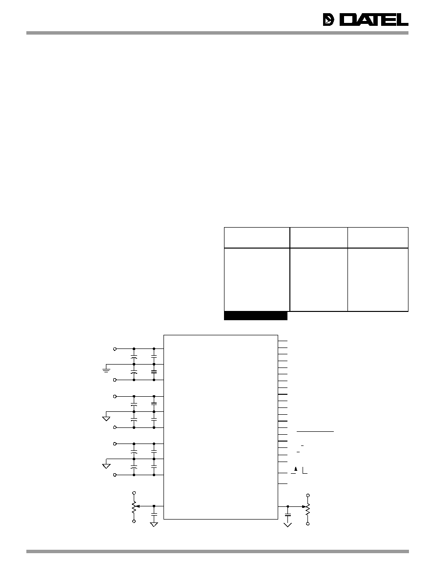
TECHNICAL NOTES
1. Obtaining fully specified performance from the ADS-945
requires careful attention to pc-card layout and power
supply decoupling. The device's analog and digital ground
systems are connected to each other internally. For optimal
performance, tie all ground pins directly to a large analog
ground plane beneath the package.
Bypass all power supplies to ground with 10
µ
F tantalum
capacitors in parallel with 0.1
µ
F ceramic capacitors. The
bypass capacitors should be located as close to the
unit as possible.
2. The ADS-945 achieves its specified accuracies without the
need for external calibration. If required, the device's small
initial offset and gain errors can be reduced to zero using
the adjustment circuitry shown in Figure 2. The typical
adjustment range is ±0.2%FSR for this circuitry.
When using this circuitry, or any similar offset and gain-
calibration hardware, make adjustments following warmup.
To avoid interaction, always adjust offset before gain.
3. To enable the three-state outputs, apply a logic "0" (low) to
OUTPUT ENABLE (pin 34). To disable, apply a logic "1"
(high) to pin 34.
4. A passive bandpass filter (Allen Avionics F4202 Series) is
used at the input of the A/D for all production testing.
5. The ADS-945's digital outputs should not be directly
connected to a noisy data bus. Drive the bus with 573 or
574 type latches and use "low-noise" logic, such as the
74LS series.
ADS-945
4
Æ
Æ
CALIBRATION PROCEDURE
(Refer to Figure 2 and Table 1)
Note: Connect pin 18 to ANALOG GROUND (pin 19) for
operation without zero/offset adjustment. Connect pin 9 to
ANALOG GROUND (pin 8) for operation without gain
adjustment.
Any offset and/or gain calibration procedures should not be
implemented until devices are fully warmed up. To avoid
interaction, offset must be adjusted before gain. The ranges of
adjustment for the circuit in Figure 2 are guaranteed to
compensate for the ADS-945's initial accuracy errors and may
not be able to compensate for additional system errors.
A/D converters are calibrated by positioning their digital
outputs exactly on the transition point between two adjacent
digital output codes. This can be accomplished by connecting
LED's to the digital outputs and adjusting until certain LED's
"flicker" equally between on and off. Other approaches
employ digital comparators or microcontrollers to detect when
the outputs change from one code to the next.
For the ADS-945, offset adjusting is normally accomplished at
the point where the MSB is a 1 and all other output bits are 0's
and the LSB just changes from a 0 to a 1. This digital output
transition ideally occurs when the applied analog input is
+Ω LSB (+76.3
µ
V).
Gain adjusting is accomplished when all bits are 0's and the
LSB just changes from a 0 to a 1. This transition ideally
occurs when the analog input is at +full scale minus 1 Ω LSB's
(+1.249771V) .
Note: Due to inherent system noise, the averaging of
several
conversions may be needed to accurately
adjust both offset
and gain to 1LSB of accuracy.
Zero/Offset Adjust Procedure
1. Apply a train of pulses to the START CONVERT input
(pin 32) so the converter is continuously converting.
2. Apply +76.3
µ
V to the ANALOG INPUT (pin 4).
3. Adjust the offset potentiometer until the output bits are
10 0000 0000 0000 and the LSB flickers between 0 and 1.
Gain Adjust Procedure
1. Apply +1.249771V to the ANALOG INPUT (pin 4).
2. Adjust the gain potentiometer until all output bits are 0's
and the LSB flickers between 0 and 1.
3. To confirm proper operation of the device, vary the applied
input voltage to obtain the output coding listed in Table 1.
Note: A single +5V supply can be used for both the +5V
ANALOG and the +5V DIGITAL. If separate supplies are
used, the difference between the two can not exceed
100mV. This also applies to the ≠5.2V supply requirements.
Datel recommends using ferrite beads to separate the analog
and digital supplies (FAIR-RITE # 2643000301.)
Figure 2. ADS-945 Connection Diagram
OUTPUT CODING
INPUT RANGE
BIPOLAR
MSB
LSB
±1.25V
SCALE
00 0000 0000 0000
+1.249847
+FS ≠1 LSB
00 0111 1111 1111
+0.937500
+3/4 FS
00 1111 1111 1111
+0.625000
+1/2FS
01 1111 1111 1111
0.000000
0
10 1111 1111 1111
≠0.625000
≠1/2FS
11 0111 1111 1111
≠0.937500
≠3/4FS
11 1111 1111 1110
≠1.249847
≠FS +1 LSB
11 1111 1111 1111
≠1.250000
≠FS
COMP. OFF. BINARY
Table 1. Output Coding
ADS-945
20k
53
52
51
50
49
48
47
46
45
44
43
42
41
40
34
33
30
29
4
BIT 1 (MSB)
BIT 2
BIT 3
BIT 4
BIT 5
BIT 6
BIT 7
BIT 8
BIT 9
BIT 10
BIT 11
BIT 12
BIT 13
BIT 14 (LSB)
OUTPUT ENABLE
OVERFLOW
T/H STATUS
T/H STATUS
ANALOG INPUT
ANALOG
SUPPLY
DIGITAL
SUPPLY
55
54
58-60
OFFSET
ADJUST
18
0.1µF
10µF
64-68
63
0.1µF
10µF
69
+
+
≠5.2V
+5V
32
START CONVERT
7
+10 REF. OUT
0.1µF
10µF
0.1µF
10µF
+
+
≠5.2V
+5V
57
0.1µF
10µF
13
15-17
13
0.1µF
10µF
12
+
+
≠15V
+15V
DIGITAL
SUPPLY
ANALOG
SUPPLY
0.1µF
9
GAIN
ADJUST
20k
DIGITAL
GROUND
ANALOG
GROUND
ANALOG
GROUND
≠15V
+15V
+15V
≠15V
ADS-945
5
Æ
Æ
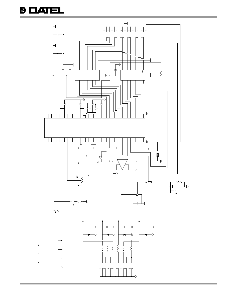
Figure 3.
ADS-945 Ev
aluation Boar
d Sc
hematic (D
A
TEL Dwg.
#A-23442)
A
L
L
CH
OK
ES
AR
E
AL
L D
I
O
D
ES
A
R
E
A
L
L
NO
N P
O
L
O
R
I
Z
E
D CA
PA
C
I
T
O
R
S
A
R
E
ALL P
O
LO
RIZE
D C
A
P
A
C
I
TO
RS
AR
E
AL
L
S
W
ITC
H
ES
AR
E SH
OW
N I
N
TH
E
1.
LA
TC
HE
S
DA
T
A
0.1" G
R
I
D
H
O
LE
PA
TT
ER
N
-5
.2
V
A
-5
.2
V
-
1
5
V
+1
5V
+5
VA
+5
V
-5
.2
V
+5
V
+5
V
-V
+V
+1
5V
-1
5
V
-5
.2
V
A
+5
VA
+5
VD
(
L
SB)
BIT 1
4
BIT 1
3
BIT 1
2
BIT 1
1
BIT 1
0
BIT 9
BIT 8
BIT 7
BIT 6
BIT 5
BIT 4
BIT 1
BIT 3
BIT 2
(M
S
B
)
-5
.2
V
D
-5
.2
V
A
+5
VA
OS
3
EN
AB
LE
CL
O
C
K
T/H
T/H
O
FFS
ET
+1
5V
-1
5
V
GA
I
N
VR
EF
IN
+
+5
V
CP
OC
GN
D
+5
V
Q8
Q7
Q6
Q5
Q4
Q3
Q2
Q1
3D
8D
7D
6D
5D
4D
2D
1D
CP
OC
GN
D
+5
V
Q8
Q7
Q6
Q5
Q4
Q3
Q2
Q1
3D
8D
7D
6D
5D
4D
2D
1D
+
+
-1
5
V
-1
5
V
+1
5V
+1
5V
NO
T
E
S
:
+
+
-
1
5V/80M
A
+1
5V/
5
0M
A
+1
5V
-1
5
V
-5
.2
V
+5
VD
+5
VA
-5
.2
V
D
-5
.2
V
A
+5
VA
+5
VD
-5
.2
V
D
-5
.2
V
A
+5
VA/350M
A
O.
F
.
2.
3.
U
N
LE
SS
OT
HE
RW
I
S
E S
PEC
I
F
I
E
D
.
AL
L R
E
S
I
ST
OR
S A
R
E
I
N
O
H
M
S
R
N
55
C.
10UF
D 25V.
0.1UF
D
50V
.
1N
400
1.
2U
HY
.
N
.
C. PO
SI
T
I
O
N
.
C
9
N
O
T
TO
BE
I
N
ST
ALL
E
D
.
I
N
ST
ALL
I
N
SO
CK
ET
(
I
T
E
M
34
)
.
FO
R
X1
US
E M
O
N
I
T
O
R
OS
CILLA
TO
R T
Y
P
E
970T
,
4
.
R
E
M
O
V
E
X
1
IF
U
S
IN
G
E
X
T
E
R
N
A
L
C
L
O
C
K
.
DN
C
U4
C2
6
C2
3
C2
2
C1
7
C1
6
C1
5
C1
4
C9
C2
1
C2
0
C1
9
C1
8
U1
C2
9
C2
8
C2
7
U7
U6
C2
C1
D1
L2
L1
JP
R1
JP
R2
P2
P1
X1
R2
R1
P4
R1
2
51
.
1
R3
L1
1
L1
0
L3
L4
L5
L6
NC
R5
L7
D2
D3
C3
D4
C4
JP
R3
SG
3
SG
1
SG
2
SG
4
P3
D
D
D
D
D
D
EX
T
IN
T
IN
T
EX
T
CO
NN
EC
T
O
R
CO
NN
EC
T
O
R
8
1,7
14
CW
O
FFS
ET
CW
GA
I
N
EX
T.
CL
OC
K
M
SB BI
T
1
BI
T
9
BI
T
1
0
BI
T
1
1
BI
T
1
2
BI
T
1
3
LS
B B
I
T
14
O
VER
FL
OW
CL
O
C
K
EO
C
BI
T
8
BI
T
7
BI
T
6
BI
T
5
BI
T
4
BI
T
3
BI
T
2
EN
AB
L
E
AG
ND
AG
ND
DG
ND
DG
ND
LT
101
6
10
PF
AD
S9
45
AL
S57
3
AL
S57
3
O
U
TP
UT
EN
AB
LE
CL
O
C
K
D
A
TA
O
U
TP
UT
PO
W
E
R
SU
PP
LY
10
M
H
Z
20
K
20
K
10
K
51
.
1
(O
P
T
)
8
7
6
5
4
3
2
1
76
75
74
73
72
71
70
69
68
67
66
65
64
63
62
61
60
59
58
57
56
55
54
53
52
51
50
49
48
47
46
45
44
43
42
41
40
39
38
37
36
35
34
33
32
31
30
29
28
27
26
25
24
23
22
21
20
19
18
17
16
15
14
13
12
11
10
9
8
7
6
5
4
3
2
1
20
12
9
81
3
14
7
61
5
11
10
16
5
41
7
18
3
21
9
1
20
12
9
81
3
14
7
61
5
11
10
16
5
41
7
18
3
21
9
1
3
2
1
3
2
1
2
34
33
32
31
30
29
28
27
26
25
24
23
22
21
20
19
18
17
16
15
14
13
12
11
10
9
87
65
43
21
26
25
24
23
22
21
20
19
18
17
16
15
14
13
12
11
10
9
87
65
43
21
3
2
1
3
2
1
1
3