1
OFFSET ADJUST V1
2
OFFSET ADJUST I1
3
ANALOG INPUT 1
4
ANALOG INPUT 2
5
ANALOG GROUND
6
S/H1 OUT
7
S/H1 ROUT
8
S/H2 SUMMING NODE
9
OFFSET ADJUST V2
10
OFFSET ADJUST I2
11
S/H1 COMMAND
12
S/H2 COMMAND
INPUT/OUTPUT CONNECTIONS
24
+15V ANALOG SUPPLY
23
ANALOG GROUND
22
V OUT
21
ANALOG GROUND
20
A/D CLOCK2
19
A/D CLOCK2
18
A/D CLOCK1
17
A/D CLOCK1
16
+5V DIGITAL SUPPLY
15
DIGITAL GROUND
14
ANALOG GROUND
13
�15V ANALOG SUPPLY
FEATURES
��
��
�
Use with 10 to 14-bit A/D converters
��
��
�
1.25 Megapixels/second minimum throughput (14 bits)
��
��
�
�10V input/output ranges, Gain = �1
��
��
�
Low noise, 200�Vrms
��
��
�
Two independent S/H amplifiers
��
��
�
Gain matching between S/H's
��
��
�
Offset adjustments for each S/H
��
��
�
Four external A/D control lines
��
��
�
Small package, 24-pin ceramic DDIP
��
��
�
Low power, 700mW
��
��
�
Low cost
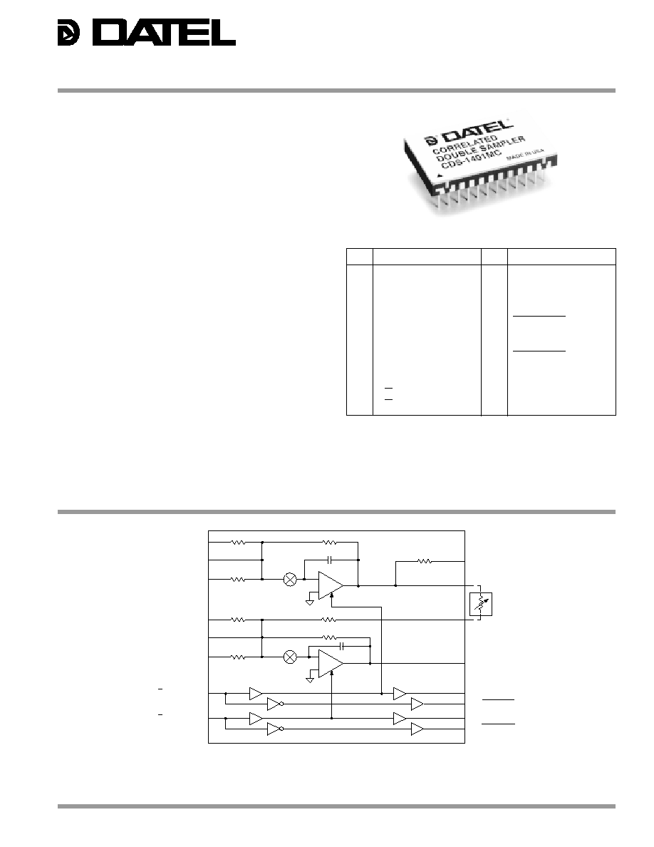
GENERAL DESCRIPTION
The CDS-1401 is an application-specific, correlated double
sampling (CDS) circuit designed for electronic-imaging
applications that employ CCD's (charge coupled devices) as
their photodetector. The CDS-1401 has been optimized for
use in digital video applications that employ 10 to 14-bit A/D
converters. The low-noise CDS-1401 can accurately
determine each pixel's true video signal level by sequentially
sampling the pixel's offset signal and its video signal and
subtracting the two. The result is that the consequences of
residual charge, charge injection and low-frequency "kTC"
noise on the CCD's output floating capacitor are effectively
eliminated. The CDS-1401 can also be used as a dual
sample-hold amplifier in a data acquisition system.
The CDS-1401 contains two sample-hold amplifiers and
appropriate support/control circuitry. Features include
independent offset-adjust capability for each S/H, adjustment
for matching gain between the two S/H's, and four control
PIN
FUNCTION
PIN
FUNCTION
INNOVATION and EX C ELL E N C E
�
�
Figure 1. CDS-1401 Functional Block Diagram
lines for triggering the A/D converter used in conjunction with
the CDS-1401. The CDS circuit's "ping-pong" timing
approach (the offset signal of the "n+1" pixel can be acquired
while the video output of the "nth" pixel is being converted)
guarantees a minimum throughput, in a 14-bit application, of
1.25MHz. In other words, the true video signal (minus offset)
will be available
(continued on page 4-5)
CDS-1401
14-Bit, Fast-Settling
Correlated Double Sampling Circuit
S/H 2
OFFSET ADJUST V1 1
OFFSET ADJUST I1 2
ANALOG INPUT 1 3
S/H 1
OFFSET ADJUST V2 9
OFFSET ADJUST I2 10
ANALOG INPUT 2 4
S/H1 COMMAND 11
S/H2 COMMAND 12
5, 14, 21, 23
ANALOG GROUND
24
+15V SUPPLY
16
+5V DIGITAL
SUPPLY
15
DIGITAL
GROUND
7 S/H1 ROUT
8 S/H2
SUMMING NODE
22 V OUT
18 A/D CLOCK 1
6 S/H1 OUT
OPTIONAL
17 A/D CLOCK 1
19 A/D CLOCK 2
20 A/D CLOCK 2
C
H
= 100pF
1k
100
100k
1k
C
H
= 100pF
100k
1k
900
1k
13
�15V SUPPLY
�
+
�
+
DATEL, Inc., 11 Cabot Boulevard, Mansfield, MA 02048-1151 (U.S.A.)
�
Tel: (508) 339-3000 Fax: (508) 339-6356
�
For immediate assistance (800) 233-2765
2
CDS-1401
�
�
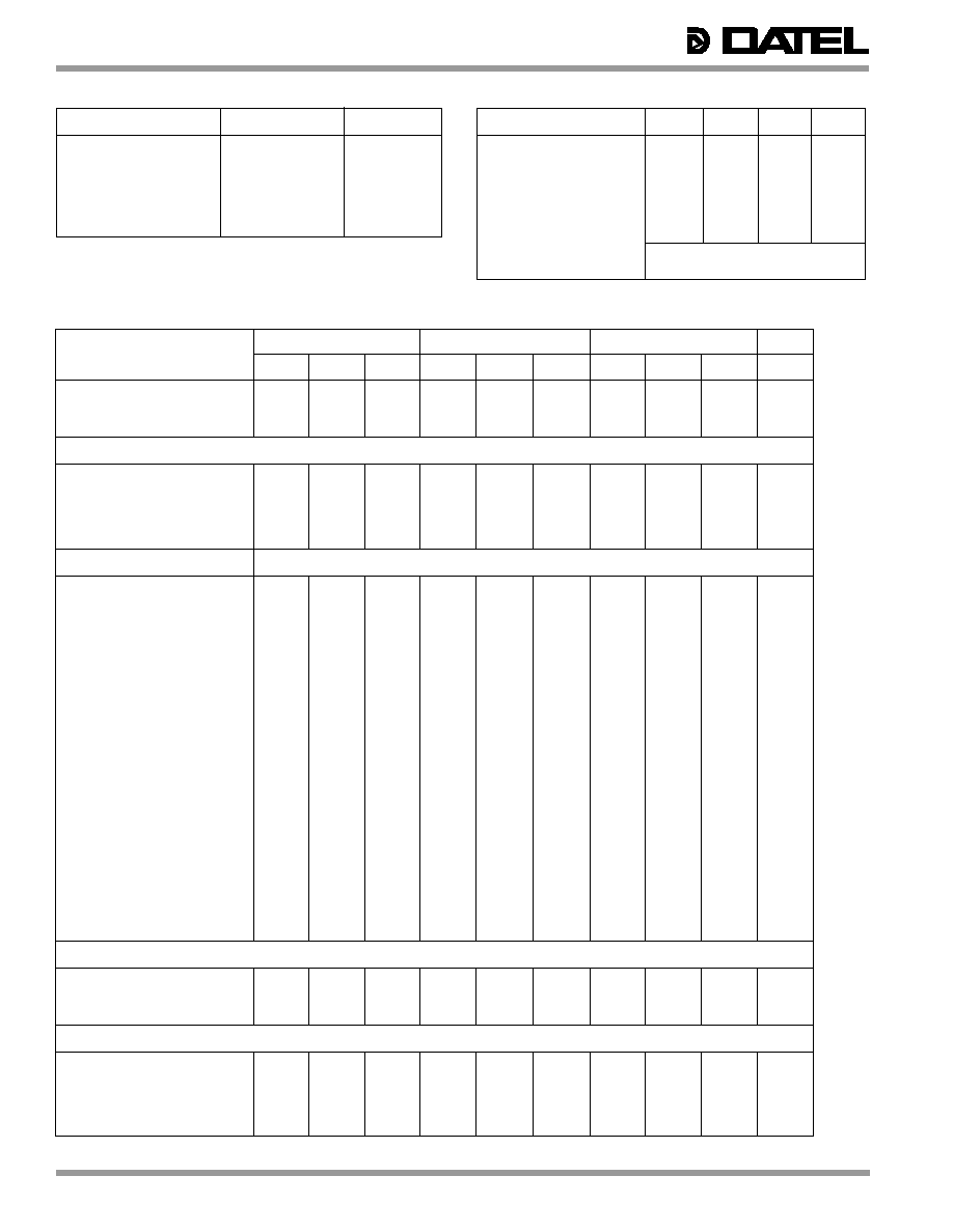
PARAMETERS
MIN.
TYP.
MAX.
UNITS
Operating Temp. Range, Case
CDS-1401MC
0
--
+70
�C
CDS-1401MM
�55
--
+125
�C
Thermal Impedance
jc
--
5
--
�C/W
ca
--
22
--
�C/W
Storage Temperature Range
�65
--
+150
�C
Package Type
24-pin, metal-sealed, ceramic DDIP
Weight
0.42 ounces(12 grams)
+25�C
0 to +70�C
�55 to +125�C
ANALOG INPUTS
MIN.
TYP.
MAX.
MIN.
TYP.
MAX.
MIN.
TYP.
MAX.
UNITS
Input Voltage Range
�10
--
--
�10
--
--
�10
--
--
Volts
Input Resistance
--
1000
--
--
1000
--
--
1000
--
Ohms
Input Capacitance
--
7
15
--
7
15
--
7
15
pF
DIGITAL INPUTS
Logic Levels
Logic "1"
+2
--
--
+2
--
--
+2
--
--
Volts
Logic "0"
--
--
+0.8
--
--
+0.8
--
--
+0.8
Volts
Logic Loading "1"
--
--
+10
--
--
+10
--
--
+10
�A
Logic Loading "0"
--
--
�10
--
--
�10
--
--
�10
�A
PERFORMANCE
Sample Mode Offset Error - S/H1
--
�1
�10
--
�2
�10
--
�4
�10
mV
Gain Error - S/H1
--
�0.2
�1
--
�0.25
�1
--
�0.3
�1.5
%
Pedestal - S/H1
--
�15
�35
--
�15
�35
--
�15
�35
mV
Sample Mode Offset Error - S/H2
--
�1
�10
--
�2
�10
--
�4
�10
mV
Gain Error - S/H2
--
�0.2
�1
--
�0.25
�1
--
�0.3
�1.5
%
Pedestal - S/H2
--
�15
�35
--
�15
�35
--
�15
�35
mV
Sample Mode Offset Error - CDS
--
�1
�10
--
�2
�10
--
�4
�10
mV
Differential Gain Error - CDS
--
�0.25
�1
--
�0.3
�1
--
�0.35
�1.5
%
Pedestal - CDS
--
�15
�35
--
�15
�35
--
�15
�35
mV
Pixel Rate (14-bit settling)
1.25
--
--
1.25
--
--
1.25
--
--
MHz
Input Bandwidth, �5V
Small Signal (�20dB input)
--
7
--
--
7
--
--
7
--
MHz
Large Signal (�0.5dB input)
--
5
--
--
5
--
--
5
--
MHz
Slew Rate
--
�80
--
--
�80
--
--
�80
--
V/�s
Aperture Delay Time
--
10
--
--
10
--
--
10
--
ns
Aperture Uncertainty
--
5
--
--
5
--
--
5
--
ps rms
S/H Acquisition Time
(to �0.003%, 10V step)
--
340
400
--
350
400
--
350
400
ns
Hold Mode Settling Time
(to �0.15mV)
--
TBD
--
--
TBD
--
--
TBD
--
ns
Noise
--
200
--
--
200
--
--
200
--
�Vr ms
Feedthrough Rejection
--
72
--
--
72
--
--
72
--
dB
Overvoltage Recovery Time
--
400
--
--
400
--
--
400
--
ns
S/H Saturation Voltage
--
�12.5
--
--
�12.5
--
--
�12.5
--
Volts
Droop Rate
--
�0.004
�0.02
--
�0.4
�2
--
�0.8
�4
mV/�s
ANALOG OUTPUTS
Output Voltage Range
�10
--
--
�10
--
--
�10
--
--
Volts
Output Impedance
--
0.5
--
--
0.5
--
--
0.5
--
Ohms
Output Current
--
--
�20
--
--
�20
--
--
�20
mA
DIGITAL OUTPUTS
Logic Levels
Logic "1"
+3.9
--
--
+3.9
--
--
+3.9
--
--
Volts
Logic "0"
--
--
+0.4
--
--
+0.4
--
--
+0.4
Volts
Logic Loading "1"
--
--
�4
--
--
�4
--
--
�4
mA
Logic Loading "0"
--
--
+4
--
--
+4
--
--
+4
mA
ABSOLUTE MAXIMUM RATINGS
PARAMETERS
LIMITS
UNITS
+15V Supply (Pin 24)
0 to +16
Volts
�15V Supply (Pin 13)
0 to �16
Volts
+5V Supply (Pin 16)
0 to +6
Volts
Digital Inputs (Pins 11, 12)
�0.3 to +V
DD
+0.3
Volts
Analog Inputs (Pins 3, 4)
�12
Volts
Lead Temp. (10 seconds)
300
�C
Pins 3 and 4.
See Figure 4 for relationship between input voltage, accuracy, and acquisition time.
Pins 6 and 22.
FUNCTIONAL SPECIFICATIONS
(T
A
= +25�C, �Vcc = �15V, +V
DD
= +5V, pixel rate = 1.25MHz, and a minimum warmup time of two minutes unless otherwise noted.)
PHYSICAL/ENVIRONMENTAL
3
�
�
CDS-1401
+25�C
0 to +70�C
�55 to +125�C
POWER REQUIREMENTS
MIN.
TYP.
MAX.
MIN.
TYP.
MAX.
MIN.
TYP.
MAX.
UNITS
Power Supply Ranges
+15V Supply
+14.75
+15.0
+15.25
+14.75
+15.0
+15.25
+14.75
+15.0
+15.25
Volts
�15V Supply
�14.75
�15.0
�15.25
�14.75
�15.0
�15.25
�14.75
�15.0
�15.25
Volts
+5V Supply
+4.75
+5.0
+5.25
+4.75
+5.0
+5.25
+4.75
+5.0
+5.25
Volts
Power Supply Currents
+15V Supply
--
+23
+27
--
+23
+27
--
+23
+27
mA
�15V Supply
--
�23
�27
--
�23
�27
--
�23
�27
mA
+5V Supply
--
+1
+2
--
+1
+2
--
+1
+2
mA
Power Dissipation
--
700
850
--
700
850
--
700
850
mW
Power Supply Rejection
--
100
--
--
100
--
--
100
--
dB
focal plane arrays, charge coupled devices, etc.) have unique
output characteristics that call for specific analog-signal-
processing (ASP) functions at their outputs. Charge coupled
devices (CCD's), in particular, display a number of unique
characteristics. Among them is the fact that the "offset error"
associated with each individual pixel (i.e., the apparent
photonic content of that pixel after having had no light incident
upon it) changes each and every time that particular pixel is
accessed.
Most of us think of an offset as a constant parameter that
either can be compensated for (by performing an offset
adjustment) or can be measured, recorded, and subtracted
from subsequent readings to yield more accurate data.
Contending with an offset that varies from reading to reading
requires measuring and recording (or capturing and storing)
the offset each and every time, so it can be subtracted from
each subsequent data reading.
The "double sampling" aspect of CDS refers to the operation of
sampling and storing/recording a given pixel's offset and then
sampling the same pixel's output an instant later (with both the
offset and the video signal present) and subsequently
subtracting the two values to yield what is referred to as the
"valid video" output for that pixel.
The "correlated" in CDS refers to the fact that the two samples
must be taken close together in time because the offset is
constantly varying. Reasons for this phenomena are
discussed below.
At the output of all CCD's, transported pixel charge (electrons)
is converted to a voltage by depositing the charge onto a
capacitor (usually called the output or "floating" capacitor).
The voltage that develops across this capacitor is obviously
proportional to the amount of deposited charge (i.e., the
number of electrons) according to
V =
Q/C. Once settled,
the resulting capacitor voltage is buffered and brought to the
CCD's output pin as a signal whose amplitude is proportional
to the total number of photons incident upon the relevant pixel.
After the output signal has been recorded, the floating
capacitor is discharged ("reset", "clamped", "dumped") and
made ready to accept charge from the next pixel. This is
when the problems begin. (This is a somewhat oversimplified
FUNCTIONAL DESCRIPTION
Correlated Double Sampling
All photodetector elements (photodiodes, photomultiplier tubes,
GENERAL DESCRIPTION
(continued)
at the output of the CDS-1401 every 800ns. This correlates
with the fact that an acquisition time of 400ns is required for
each internal S/H amplifier (10V step setting to �0.003%). The
input and output of the CDS-1401 can swing up to �10 Volts.
The functionally complete CDS-1401 is packaged in a single,
24-pin, ceramic DDIP. It operates from �15V and +5V supplies
and consumes 700mW. Though the CDS-1401's approach to
CDS appears straightforward (see Description of Operation),
the circuit actually exploits an elegant architecture whose
tradeoffs enable it to offer wide-bandwidth, low-noise and high-
throughput combinations unachievable until now. The CDS-
1401 is a generic type of circuit that can be used with almost
any 10 to 14-bit A/D converter. However, DATEL does offer
A/D converters that are optimized for use with the CDS-1401.
TECHNICAL NOTES
1. To achieve specified performance, all power supply pins
should be bypassed with 2.2�F tantalum capacitors in
parallel with 0.1�F ceramic capacitors. All ANALOG
GROUND (pins 5, 14, 21 and 23) and DIGITAL GROUND
(pin 15) pins should be tied to a large analog ground plane
beneath the package.
2. In the CDS configuration, to avoid saturation of the S/H
amplifiers, the maximum analog inputs and conditions are
as follows:
ANALOG INPUT 1 < �12V
(ANALOG INPUT 1 � ANALOG INPUT 2) < �12V
3. The combined video and reference/offset signal from the
CCD array must be applied to S/H2, while the reference/
offset signal is applied to S/H1.
4. To use as a CDS circuit, tie pin 8 (S/H2 SUMMING NODE)
to either pin 6 (S/H1 OUT), through a 200 Ohm
potentiometer, or directly to pin 7 (S/H1 ROUT). In both
cases, the CCD's output is tied to pins 3 (ANALOG INPUT
1) and 4 (ANALOG INPUT 2). As shown in Figure 5, the
200
potentiometer is for gain matching.
5. To use as a dual S/H, leave pin 7 (S/H1 ROUT) and pin 8
(S/H2 SUMMING NODE) floating. Pin 6 (S/H1 OUT) will be
the output of S/H1 and pin 22 (V OUT) will be the output
of S/H2.
6. See Figure 4 for acquisition time versus accuracy and input
voltage step amplitude.
4
CDS-1401
�
�
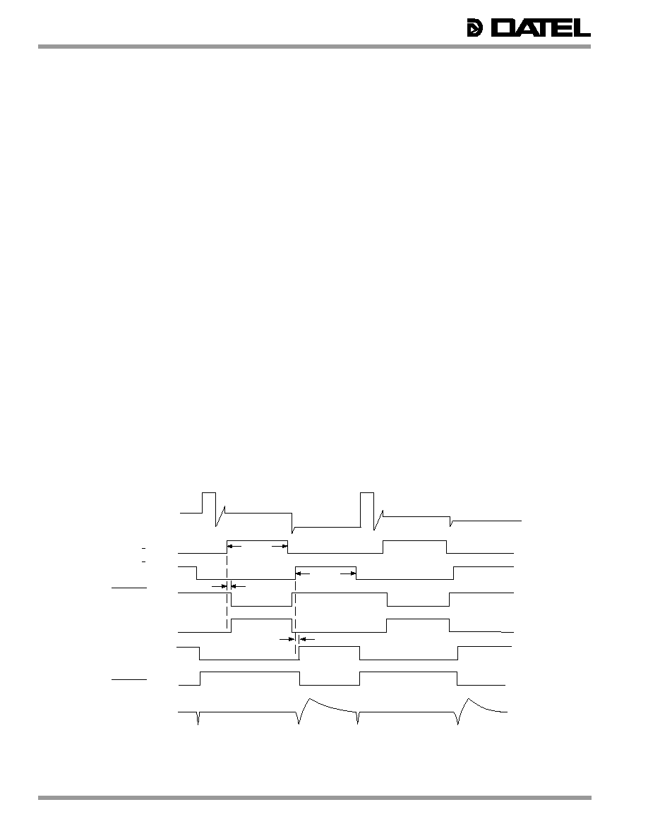
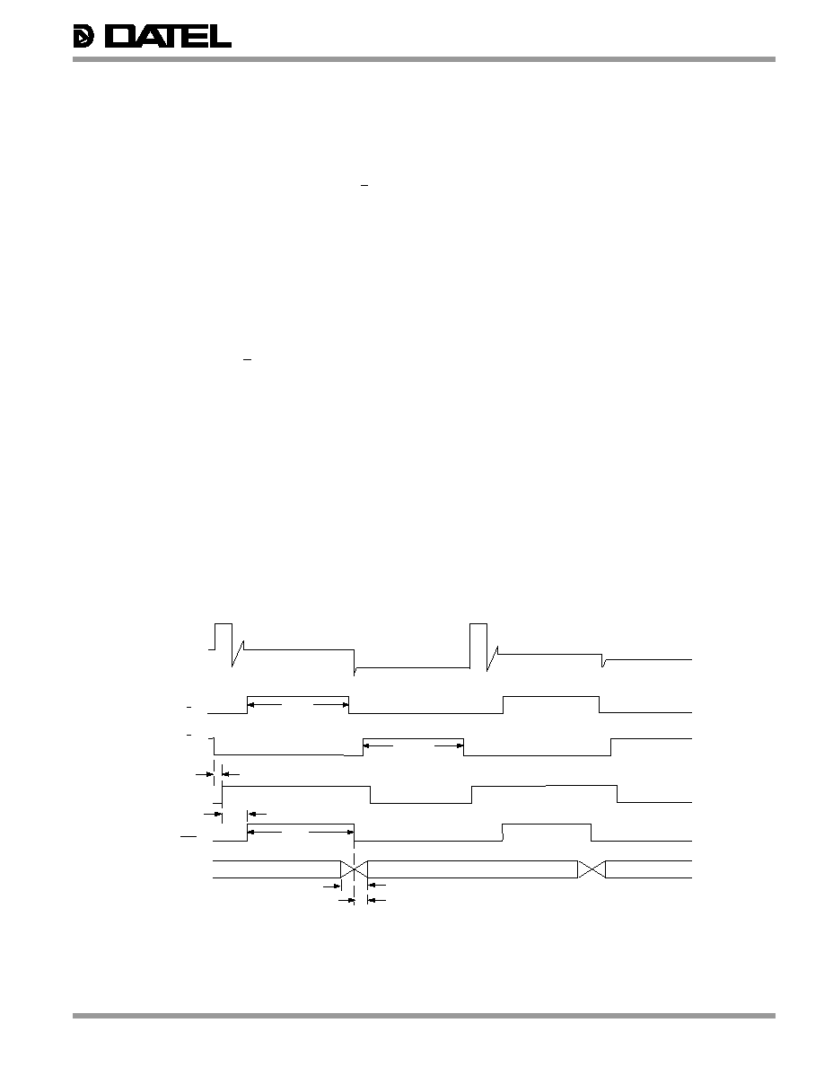
Figure 2. CDS-1401 Typical Timing Diagram
explanation in that the floating capacitor is not usually
"discharged" but, in fact, "recharged" to some predetermined
dc voltage, usually called the "reference level". The pixel offset
appears as an output deviation from that reference level.)
The floating capacitor is normally discharged (charged) via a
shunt switch (typically a FET structure) that has a non-zero
"on" resistance. When the switch is on, its effective series
resistance exhibits thermal noise (Johnson noise) due to the
random motion of thermally energized charge. Because the
shunt switch is in parallel with the floating capacitor, the
instantaneous value of the thermal noise (expressed in either
Volts or electrons) appears across the cap. When the shunt
switch is opened, charge/voltage is left on the floating cap.
The magnitude of this "captured noise voltage" is a function of
absolute temperature (T), the value of the floating capacitor (C)
and Boltzman's constant (k). It is commonly referred to as
"kTC" noise.
The second contributor to the constantly varying pixel offsets
is the fact that, at high pixel rates, the floating capacitor never
has time to fully discharge (charge) during the period in which
its shunt switch is closed. There is always some "residual"
charge left on the cap, and the amount of this charge varies
as a function of what was the total charge held during the
previous pixel. This amount of residual charge is, in fact,
deterministic (if you know the previous charge and the number
of time constants in the discharge period), however, it is less
of a contributor than kTC noise.
The third major contributor to pixel offset is the fact that as the
shunt FET is turned off, the voltage across (and the charge
stored on) its parasitic junction capacitances changes. The
result is an "injection" of excess charge onto the floating cap
causing a voltage step normally called a "pedestal".
The fourth major contributor to pixel offset is a low-frequency
noise component (usually called 1/f noise or pink noise)
associated with the CCD's output buffer amplifier.
Due to all of these contributing factors, "pixel offsets" vary from
sample to sample in an inconsistent, unpredictable manner.
Traditional Approach to CDS
There are a number of techniques for dealing with the varying-
offset idiosyncrasy of CCD's. The most prevalent has been
what can be called the "sample-sample-subtract" technique.
This approach requires the use of two high-speed sample-hold
(S/H) amplifiers and a difference amplifier. The first S/H is
used to acquire and hold a given pixel's offset. Immediately
after that, the second S/H acquires and holds the same pixel's
offset+video signal. After both the S/H outputs have fully
settled, the difference amplifier subtracts the offset from the
offset+video yielding the valid video signal.
CDS-1401 Approach (See Figure 1)
The DATEL CDS-1401 takes a slightly different, though clearly
superior, approach to CDS. It can be called the "sample-
subtract-sample" approach.
Note that the CDS-1401 has been configured to offer the
greatest amount of user flexibility. Its two S/H circuits function
independently. They have separate input and output pins.
Each has its own independent control lines. The control-line
signals are delayed, buffered, and brought back out of the
ANALOG INPUT
FOR CDS (Pins 3 and
4 are tied)
S/H 1 (Pin 11)
A/D CLOCK 1 (Pin 17)
S/H 2 (Pin 12)
A/D CLOCK 1 (Pin 18)
A/D CLOCK 2 (Pin 19)
A/D CLOCK 2 (Pin 20)
VOLTAGE OUTPUT
VIDEO SIGNAL N-1
VIDEO SIGNAL N
(CCD OUTPUT)
100ns typ.
30ns typ.
30ns typ.
NOTE: Not Drawn to Scale
RESET N
OFFSET N
OFFSET +
VIDEO N
RESET N+1
OFFSET N+1
OFFSET +
VIDEO N+1
100ns typ.
HOLD
HOLD
5
�
�
CDS-1401
track mode when large, high-speed transients (normally
associated with clock edges) are occurring throughout the
system. This could result in the S/H amplifiers being driven
into saturation, and they may not recover in time to accurately
acquire their next signal.
For example, S/H1 should not be commanded into the sample
mode until all transients associated with the opening of the
shunt switch have begun to decay. Similarly, S/H2 should not
be driven into the sample mode until all transients associated
with the clocking of pixel charge onto the output capacitor have
begun to decay. Therefore, it is generally not a good practice
to use the same clock edge to drive S/H1 into hold (holding the
offset) and S/H2 into sample (to acquire the offset + video
signal).
S/H's that are in their signal-acquisition modes should be left
there as long as possible (so all signals can settle) and be
driven into their hold modes before any system transients
occur. In Figure 2, S/H1 is driven into the sample mode shortly
after the transient from the shunt switch has begun to decay.
S/H1 is then kept in the sample mode while the offset signal
and the S/H output settle. S/H1 is driven into hold just prior to
the system clock pulse(s) that transfers the next pixel charge
onto the output capacitor.
As soon as the transients/noise associated with the charge
transport begins to decay, S/H2 can be driven into the sample
mode. S/H2 can then be left in the sample mode until just
before the reset pulse for the output capacitor.
In Figure 2, S/H's 1 and 2 both have the same acquisition time.
If the pixel-to-pixel amplitude variation of offset signals is much
package so they can be used to control other circuit functions.
Each S/H has two pins for offset adjusting (if required), one for
current and one for voltage.
In normal operation, the output signal of the CCD is applied
simultaneously to the inputs (pins 3 and 4) of both S/H
amplifiers. S/H1 will normally be used to capture and hold
each pixel's offset signal. Therefore, S/H1 is initially in its
signal-acquisition mode (logic "1" applied to pin 11, S/H1
COMMAND). This is also called the sample or track mode.
Following a brief interval during which the output of the CCD
and the output of S/H1 are allowed to settle, S/H1 is driven into
its hold mode by applying a logic "0" to pin 11. S/H1 is now
holding the pixel's offset value.
In most straightforward configurations, the output of S/H1 is
connected to the summing node of S/H2 by connecting pin 7
(S/H1 ROUT) to pin 8 (S/H2 SUMMING NODE).
When the offset+video signal appears at the output of the
CCD, S/H2 is driven into its signal acquisition mode by
applying a logic "1" to pin 12 (S/H2 COMMAND).
S/H2 employs a current-summing architecture that subtracts
the output of S/H1 (the offset) from the output of the CCD
(offset+video) while acquiring only the difference signal (i.e.,
the valid video). A logic "0" subsequently applied to pin 12
drives S/H2 into its hold mode, and after a brief transient
settling time, the valid video signal appears at pin 22 (V OUT).
Timing Notes
See Figure 2, Typical Timing Diagram. It is advisable that
neither of the CDS-1401's S/H amplifiers be in their sample/
Figure 3. CDS-1401 in Front of ADS-CCD1201 at f
CLK
= 1MHz
S/H1
S/H2
START CONVERT
EOC
OUTPUT
DATA
DATA N-1 VALID
DATA N VALID
30ns typ.
90ns typ.
73ns max.
35ns max.
ANALOG INPUT
FOR CDS
(Pins 3 and 4 are tied)
(CCD OUTPUT)
DATA N+1 VALID
400ns
400ns
OFFSET (N+1)
OFFSET +
VIDEO (N+1)
OFFSET (N+2)
OFFSET +
VIDEO (N+2)
420ns
RESET
RESET